

VITESSE VSC7710WB, VSC7710X, VSC7710WD, VSC7710WC Datasheet
VITESSE
SEMICONDUCTOR CORPORATION
Advance Product Infor m a t ion
VSC7710
Photodetector/Transimpedance Amplifier
Family for Optical Communication
Features
• Integrated Photodetector/Transimpedance Amplifier Family Optimized for High Speed Optical
Communications Applications
• Integrated AGC
• Fibre Channel and Gigabit Ethernet
Part Number
VSC7710 1.25 1300 .22 75
Data Rate
(Gb/s)
Bandwidth
(MHz)
• High Bandwidth
• Low Input Noise Equivalent Power
• Single 5V Supply
Input Noise
µW rms)
(
Optically Active Area
µm diameter)
(
General Description
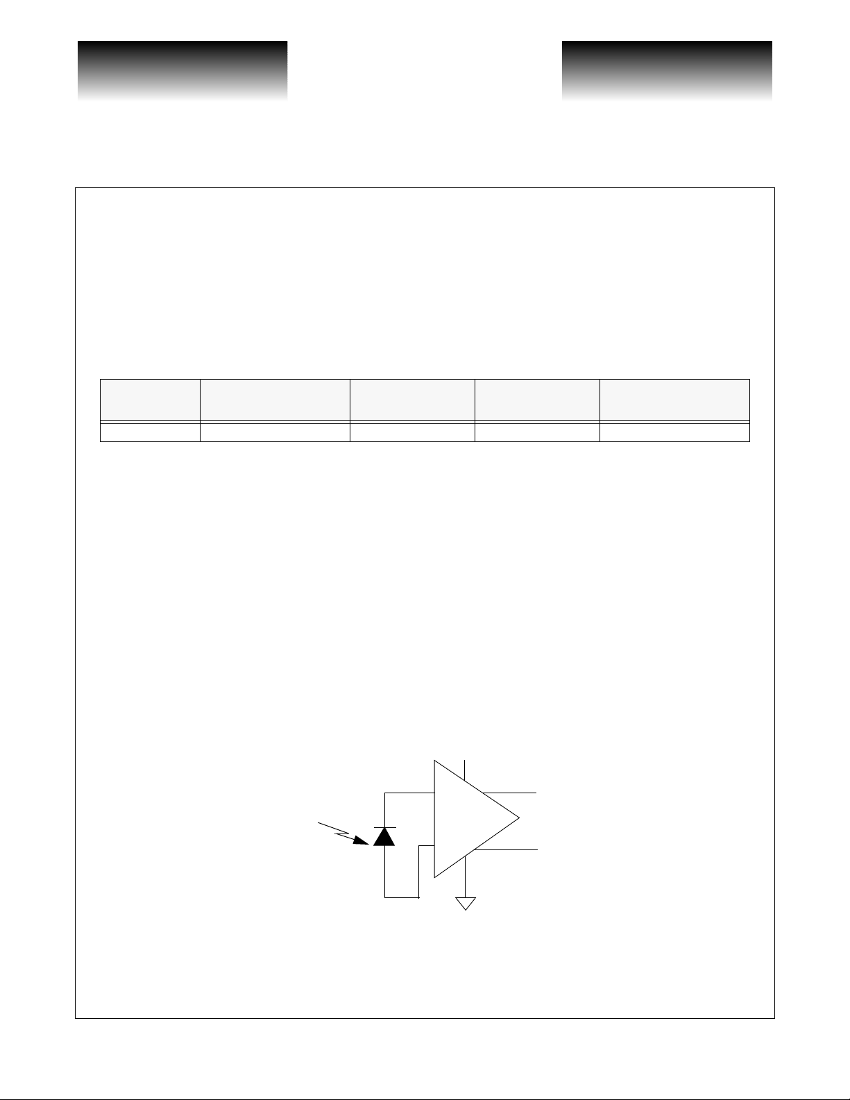
The VSC7710 integrated PIN Photodetector/Transimpedance Amplifiers provides a highly integrated solution for converting 1300 nm light from a fiber optic communications channel into a differential output voltage.
The benefits of Vitesse Semiconductor’s Gallium Arsenide H-GaAs-III process are fully utilized to provide a
very high bandwidth and low noise amplifier. The PIN detector is 75
plied internally eliminating the need for a separate bias connection. The sensi t ivit y, duty cycle distortion and jitter meet or exceed all Fibre Channel and Gigabit Ethernet application requirements. Parts are available in flatwindowed or lensed packages.
The use of a photodetector and transimpedance amplifier hybrid, reduces the input capacitance, resulting in
higher sensitivity and bandwidth and improved speed of response. These parts can easily be used in developing
Fibre Channel and Gigabit Ethernet electro-optic Receivers for the 900- 1600 nm spectra l range w hich exhibit
very high performance and ease of use.
µm in diameter. The detector bias is sup-
VSC7710 Block Diagram
+5V
+
_
G52139-0, Rev 2.2 Page 1
04/02/01
© VITESSE SEMICONDUCTOR CORPORATION • 741 Calle Plano • Camarillo, CA 93012
Tel: (800) VITESSE • FAX: (805) 987-5896 • Email: prodinfo@vitesse.c om
Internet: www.vitesse.com
D0
D1
VITESSE
SEMICONDUCTOR CORPORATION
Photodetector/Transim pe dan ce Am pl if ier
Advance Product Information
Family for Optical Communication
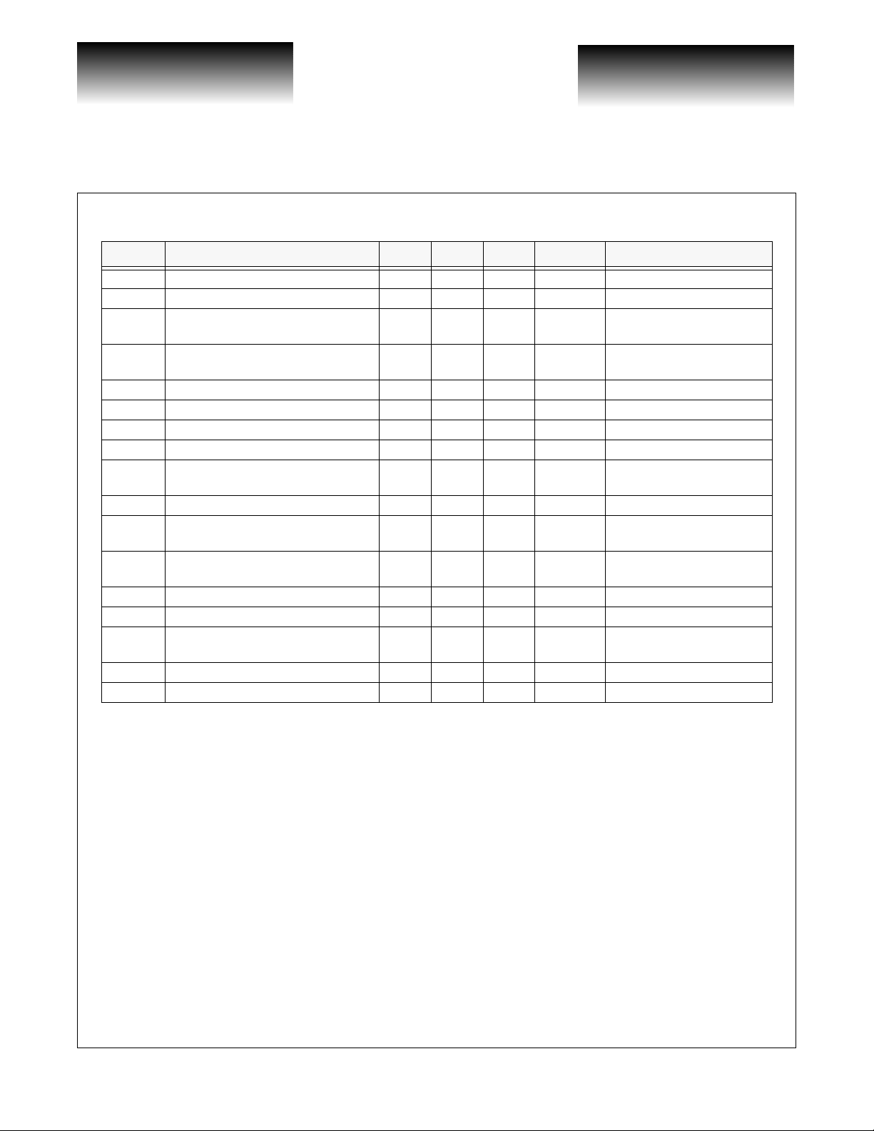
Table 1: Electro-Optic Specifications
Symbol Parameter Min Typ Max Units Conditions
V
DD
λ Wavelength 1270 1355 nm
f
c
Tr T
S Sensitivity -28 dBm BER 10
D
r
R
o
V
d
PSRR Power Supply Rejection Ratio 35 dB
I
s
BW Optical Modulation Bandwidth 700 1300 MHz
Rd Differential Responsivity 2.5 mV/µW
V
n
NEP
PDJ Pattern Dependent Jitter 60 ps
DCD Duty Cycle Distortion 5 % P = -3dBm
ýV Bias Offset Voltage 200 mV P = -3dBm
Supply Voltage 4.5 5.5 V
Low Frequency Cutoff 1.4 MHz
Rise/Fall Time 300 ps
f
Dynamic Range 25 dB
Single Ended Output I m pe da n ce 25 90 ¾
Differential Output Voltage 0.25 1.2 V P = -3 dBm, R = 100Ω
Supply Current 62 mA P = -28 to -3 dBm
Output Noise Voltage 1.2 mV
Input Noise Equivalent Optical Power 0.22 µW RMS BW = 1500MHz, P = 0mW
O
RMS
-3dB
P = -22dBm, f
20% to 80%
P = -3 dBm
f = 0.3MHz - 40MHz
Hybrid Differential
-3dB
P = -22dBm, f
ΡΛ = 100Ω
P = -22dBm f
BW = 1500MHz, P = 0mW
P = -3dBm
±10% Voltage Window
VSC7710
= 50MHz
r
-12
B = 1063Mb/s
= 50MHz
r
= 50MHz
r
Page 2 G52139-0, Rev 2.2
© VITESSE SEMICONDUCTOR CORPORATION • 741 Ca l le Pl an o • Camarillo, CA 93012
Tel: (800) VITESSE • FAX: (805) 987-5896 • Email: prodinfo@vitesse.com
Internet: www.vitesse.com
04/02/01
VITESSE
SEMICONDUCTOR CORPORATION
Advance Product Infor m a t ion
VSC7710
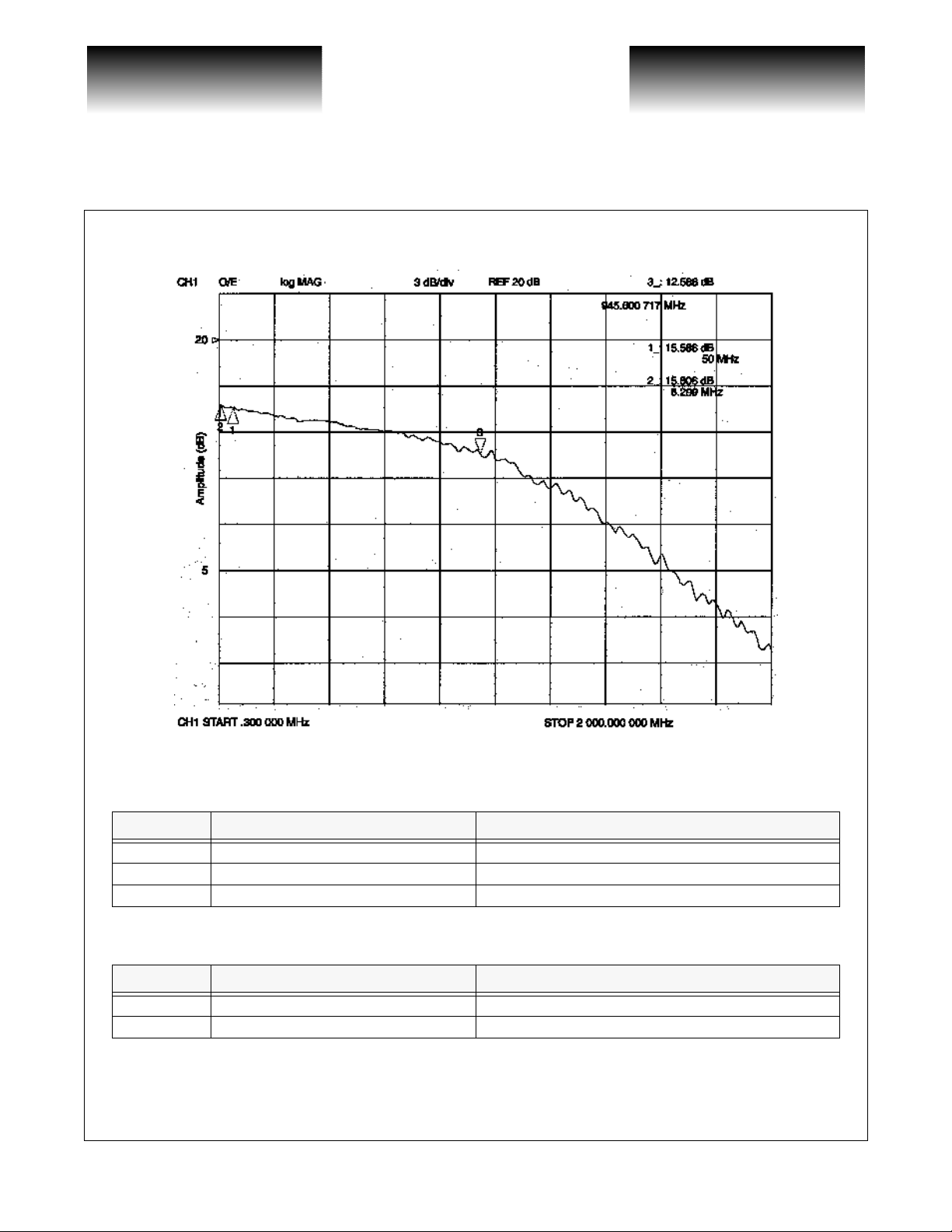
Figure 1: Amplitude vs. Frequency
Photodetector/Transimpedance Amplifier
Family for Optical Communication
Frequency response of VSC7710WB (Upper 3db frequency is measured with respect to response at 50 MHz)
Table 2: Absolute Maximum Ratings
Symbol Parameter Limits
V
DD
T
stg
P
inc
Table 3: Recommended Operating Conditions
Symbol Parameter Limits
V
DD
T
op
G52139-0, Rev 2.2 Page 3
04/02/01
Power Supply 6V
Storage Temperature -55°C to 125°C (case temperature under bias)
Incident Optical Power +3 dBm
Power Supply 4.5-5.5V (5.0V nominal)
Operating Temperature 0°C (ambient) to 70°C case
© VITESSE SEMICONDUCTOR CORPORATION • 741 Calle Plano • Camarillo, CA 93012
Tel: (800) VITESSE • FAX: (805) 987-5896 • Email: prodinfo@vitesse.com
Internet: www.vitesse.com
VITESSE
SEMICONDUCTOR CORPORATION
Photodetector/Transim pe dan ce Am pl if ier
Family for Optical Communication
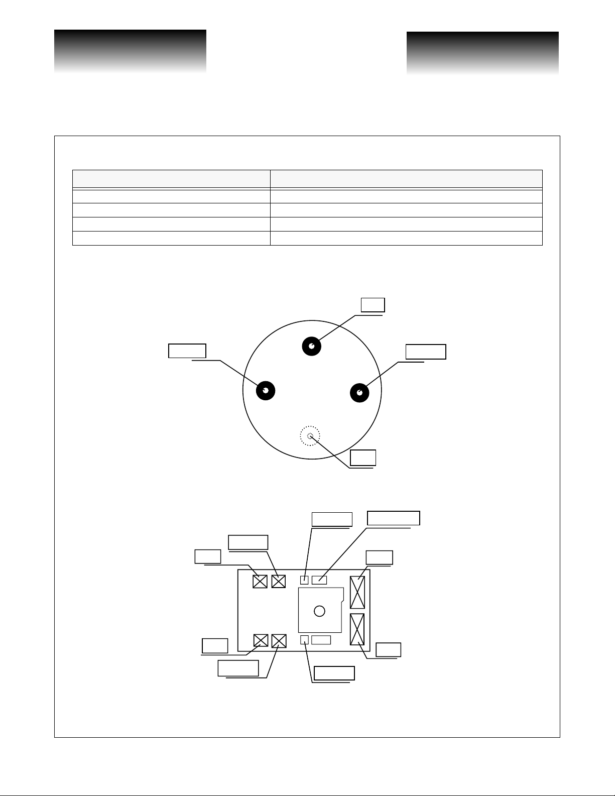
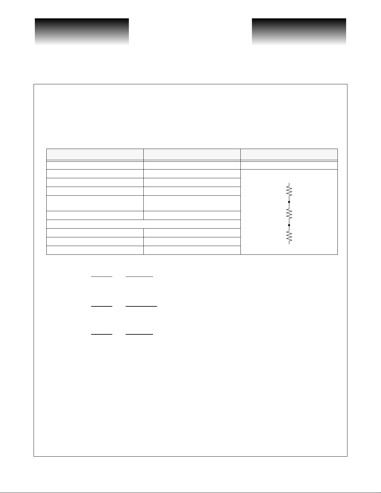
Table 4: Pin Table Specifications for TO-46(ball lens), TO-56 (flat window) Packages and Bare Die
Symbol Description
+
D
OUT
–
D
OUT
VDD Power supply
GND Ground (package case)
Note: Pin Diagram is identical for both TO-46 and TO-56 package styles.
+
D
OUT
Data output normal (with reference to incident light)
Data output complement (inverting) (with reference to incid e nt ligh t)
Figure 2: Pin Diagram
Advance Product Information
VSC7710
VDD
–
D
OUT
GND
Figure 3: Schematic View of Bare Die Pad Assignments
CATHODE
GND
VDD
GND
VDD
ANODE
–
D
OUT
+
D
OUT
ANODE
Page 4 G52139-0, Rev 2.2
© VITESSE SEMICONDUCTOR CORPORATION • 741 Ca l le Pl an o • Camarillo, CA 93012
Tel: (800) VITESSE • FAX: (805) 987-5896 • Email: prodinfo@vitesse.com
Internet: www.vitesse.com
04/02/01
VITESSE
SEMICONDUCTOR CORPORATION
Advance Product Infor m a t ion
VSC7710
Photodetector/Transimpedance Amplifier
Family for Optical Communication
Thermal Re si stance Calcu lation
In order to relate the junction temperature to an equivalent case temperature, the following thermal characteristics of the package are provided (note that the thermal conductivity is identical for TO-46 and TO-56 package styles).
Table 5: Thermal Resistance Calculation for TO-56 and TO-46 Packages.
Chip Size 0.168cm x 0.104cm Thermal Path
Chip Area A 0.015 cm
Die height (T
Epoxy thickness (T
Header thickness (Theader)
(ave. for TO-46 and TO- 56)
K GaAs 0.55W / cm °C
K epoxy 0.0186W / cm °C
K kovar 0.17W / cm °C
) 0.066 cm
die
) 0.0076 cm
epoxy
Thermal Conductivities
0.115 cm
2
T
J
θ
GaAs
θ
EXPOXY
θ
T
C
KOVAR
T
GaAsA
K
T
epoxyA
K
T
kovarA
K
die
epoxy
kovar
θ
GaAs
θ
epoxy
θ
kovar
θ
JC
= Thermal Resistance from Junction to Case = (8 + 27.24 + 47) = 82.24 °C/W
Example:
For VSC7710 at nominal supply current of 25mA and V
Temperature rise from junction to case = 0.025A x 5V x 82.24 °C/W = 10.28 °C
0.066
0.55 x 0.015
0.0076
0.0186 x 0.015
0.12
0.17 x 0.015
= 8 °C/W==
= 27.24 °C/W==
= 47 °C/W==
DD
= 5V
G52139-0, Rev 2.2 Page 5
04/02/01
© VITESSE SEMICONDUCTOR CORPORATION • 741 Calle Plano • Camarillo, CA 93012
Tel: (800) VITESSE • FAX: (805) 987-5896 • Email: prodinfo@vitesse.com
Internet: www.vitesse.com
 Loading...