

VITESSE VSC7709X, VSC7709WD, VSC7709WC, VSC7709WB, VSC7709WA Datasheet
VITESSE
SEMICONDUCTOR CORPORATION
Advance Product Information
VSC7709
1.25Gb/s Photodetector/Transimpedance
Amplifier for Optical Communication
G52362-0, Rev 2.1 Page 1
04/02/01
© VITESSE SEMICONDUCTOR CORPORATION • 741 Calle Plano • Camarillo, CA 93012
Tel: (800) VITESSE • FAX: (805) 987-5896 • Email: prodinfo@vitesse.com
Internet: www.vitesse.com
Features Applications
General Description
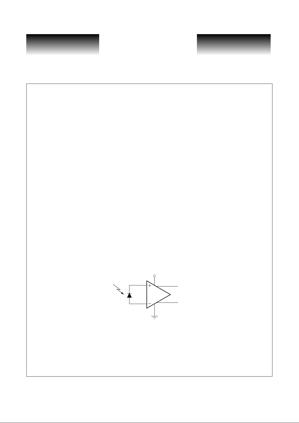
The VSC7709 integrated PIN Photodetector/Transimpedance Amplifier provides a highly integrated solution for converting 1300 nm light from a fiber optic communications channel into a differential output voltage.
The benefits of Vitesse Semiconductor’s Gallium Arsenide H-GaAs process are fully utilized to provide a very
high bandwidth and low noise a mplifier. The PIN detector is 75
µm in diameter. The detector bias is supplied
internally eliminating the need for a separate bias connection. The sens itivity, duty cycle distortion and jitter
meet or exceed all Fibre Channel and Gigabit Ethernet application requirements. The VSC7709 is available in
flat-windowed or lensed packages. The transimpedance amplifier is also available in bare die form.
The use of a photodetector and transimpedance amplifier hybrid, reduces the input capacitance, resulting in
higher sensitivity and bandwidth and improved speed of response. These parts can easily be used in developing
Fibre Channel and Gigabit Ethernet electro-optic receivers for the 900nm-1600nm spectral range which exhibit
very high performance and ease of use.
Block Diagram
• High Bandwidth: 1100MHz
• Low Input Noise Equivalent Power: 0.5mW
• Single 3.3V Supply
• 1.25Gb/s Data Rate
• 75mm Optically Active Area (PIN diode)
• Integrated AGC
• Package: TO-46, TO-56, Bare Die
+3.3V
D0
D1
• Gigabit Ethernet Optical Receivers
• Fibre Channel Optical Receivers
• ATM Optical Receivers
• System Interconnect
• SONET/SDH

VITESSE
SEMICONDUCTOR CORPORATION
Advance Product Information
VSC7709
1.25Gb/s Photodetector/ Transimpedance
Amplifier for Optical Communication
Page 2 G52362-0, Rev 2.1
04/02/01
© VITESSE SEMICONDUCTOR CORPORATION • 741 Calle Plano • Camarillo, CA 93012
Tel: (800) VITESSE • FAX: (805) 987-5896 • Email: prodinfo@vitesse.com
Internet: www.vitesse.com
Electrical Characteristics
Table 1: Electro-Optic Specifications
NOTES: (1) Applicable to packaged pa rt s with assembled 1300nm photodetect or with responsivity = 0.8A/W. (2) Applicable to bare dice.
(3) By characterization. See Measurements and Application section.
Absolute Maximum Ratings
(1)
Power Supply Voltage (VDD)...........................................................................................................................+6V
Maximum Junction Temperature Range......................................................................................-55°C to +125°C
Storage Temperature Range.........................................................................................................-55°C to +125°C
Incident Optical Power (P
INC
)....................................................................................................................+3dBm
NOTE: (1) CAUTION: Stresses listed under “Absolute Maximum Ratings” may be applied to devices one at a time without caus-
ing permanent damage. Functionality at or above the values listed is not implied. Exposure to these values for extended
periods may affect device reliability.
Recommended Operating Conditions
Positive Voltage Rail (VDD)........................................................ ..........................................................3.0 to 3.6V
Negative Voltage Rail (GND)............................................................................................................................0V
Operating Temperature Range (T
A
)...........................................................................0°C Ambient to +85°C Case
Symbol Parameter Min Typ Max Units Conditions
λ Wavelength 1270 1355 nm
V
DD
Power Supply Voltage 3.0 3.6 V
I
S
Power Supply Current 30 mA
PSRR Power Supply Rejection Ratio TBD dB
f = 0.3MHz to 40MHz. Hybrid
differential with external filter.
BW Optical Modulation Bandwidth 1000 MHz
See Measurements an d
Applications section
f
C
Low Frequency Cutoff 2 MHz
See Measurements an d
Applications section
R
D
Differential Responsivity 2.5 mV/µW
T
Z
Differential Transimpedance 2000 Ω RL = 100Ω
(1)
R
O
Single-Ended Outp ut Impedance 25 Ω RL = 100Ω
(2)
V
N
Output Noise Voltage 1.2 mV rms BW = 800MHz, P = 0mW
NEP
O
Input Noise Equivalent Optical Power 0.5 µW rms BW = 800MHz, P = 0mW
S Sensitivity -26 dBm BER 10
-12
, B = 1250Mb/s
(3)
∆V Bias Offset Voltage 200 mV P = -3dBm
V
D
Differential Output Voltage 0.25 V P = -3dBm, R = 100Ω
PDJ Pattern Dependent Jitter 60 ps
P = -3dBm, ±10% volta ge
window
DCD Duty Cycle Distortion 5 % P = -3dBm
T
R
/T
F
Rise and Fall Times 400 ps 20% to 80%, P = -3dBm
VITESSE
SEMICONDUCTOR CORPORATION
Advance Product Information
VSC7709
1.25Gb/s Photodetector/Transimpedance
Amplifier for Optical Communication
G52362-0, Rev 2.1 Page 3
04/02/01
© VITESSE SEMICONDUCTOR CORPORATION • 741 Calle Plano • Camarillo, CA 93012
Tel: (800) VITESSE • FAX: (805) 987-5896 • Email: prodinfo@vitesse.com
Internet: www.vitesse.com
Package Descriptions
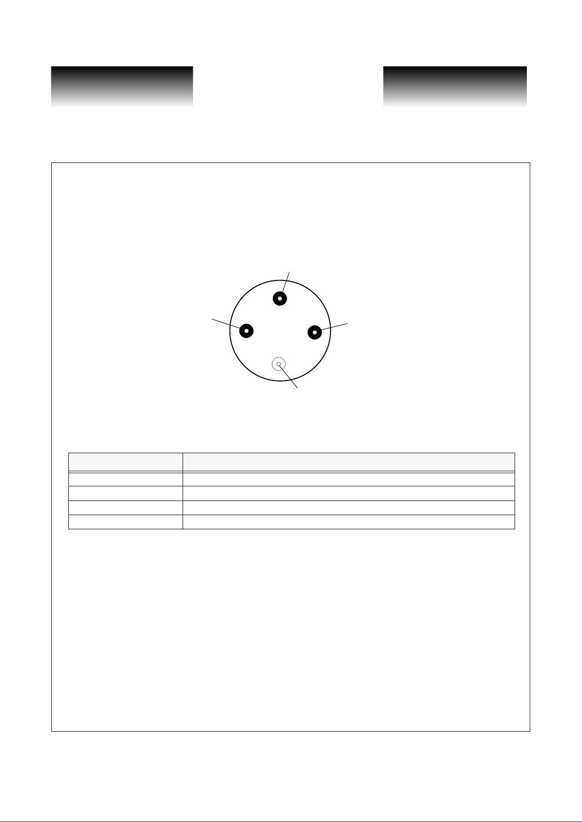
Figure 1: Pin Diagram
Table 2: Pin Identification for TO-46 (ball lens) and Bare Die
Symbol Description
D+OUT Data output normal (with reference to incident light)
D
–
OUT Data output complement (inverting, with reference to incident light)
VDD Power supply
GND Ground (package case)
VSS
DOUTN
DOUTP
GND
TO Package
BottomView
 Loading...