

VITESSE VSC7216UC-01 Datasheet
Preliminary Datasheet
VITESSE
SEMICONDUCTOR CORPORATION
VSC7216-01
Features
• 4 ANSI X3T11 Fibre Channel and IEEE 802.3z
Gigabit Ethernet Compliant Transceivers
• Over 8 Gb/s Duplex Raw Data Rate
• Redundant PECL Tx Outputs and Rx Inputs
• 8B/10B Encoder/Decoder per Channel, Optional
Encoder/Decoder Bypass Operation
• “ASIC-Friendly
Parallel Input Data
• Elastic Buffers for Intra/Inter-Chip Ca ble Deskewing
and Channel-to-Channel Alignment
• Tx/Rx Rate Matching via IDLE Insertion/Deletion
• Compatible with VSC7211/7212/7214
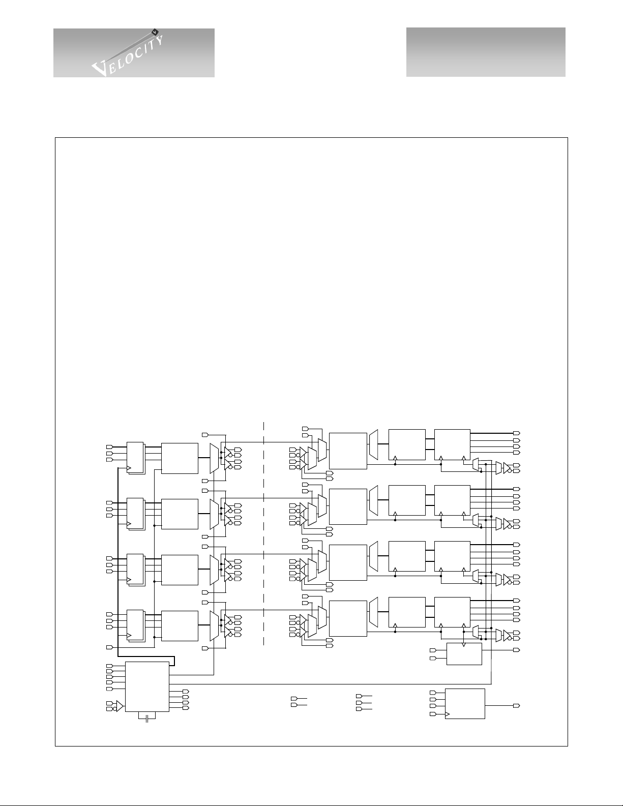
VSC7216-01 Block Diagram
C/DB
C/DA
88
DQ
88
DQ
88
DQ
88
DQ
Clock Gen
TD(7:0)
C/DD
WSEND
TC(7:0)
C/DC
WSENC
TB(7:0)
WSENB
TA(7: 0)
WSENA
KCHAR
TBCA
TBCB
TBCC
TBCD
DUAL
REFCLKP
REFCLKN
TM
” Timing Options for Transmitter
TRANSMITTER
PTXEND
8B/10B
Encode
RTXEND
PTXENC
8B/10B
Encode
RTXENC
PTXENB
8B/10B
Encode
RTXENB
PTXENA
8B/10B
Encode
4
x20/x10
CAP0 CAP1
RTXENA
Tx Clock
REFCLK
TBERRA
TBERRB
TBERRC
TBERRD
LBTXD
10
10
10
10
PTXD+
PTXDRTXD+
RTXD-
LBTXC
PTXC+
PTXCRTXC+
RTXC-
LBTXB
PTXB+
PTXBRTXB+
RTXB-
LBTXA
PTXA+
PTXARTXA+
RTXA-
LBEND(1:0)
RXP/RD
PRXD+
PRXDRRXD+
RRXD-
LBENC(1:0)
RXP/RC
PRXC+
PRXCRRXC+
RRXC-
LBENB(1:0)
RXP/RB
PRXB+
PRXBRRXB+
RRXB-
LBENA(1:0)
RXP/RA
PRXA+
PRXARRXA+
RRXA-
TMODE(2:0)
RMODE(1:0)
Multi-Gigabit Interconnect Chip
• Received Data Aligned to Local REFCLK or to
Recovered Clock
• PECL Rx Signal Detect and Cable Equalization
• Per-Channel Serial Tx-to-Rx and Parallel Rx-
to-Tx Internal Loopback Modes
• Clock Multiplier Generates Baud Rate Clock
• Automatic Lock-to-Reference
• JTAG Boundary Scan Support for TTL I/O
• Built-In Self Test
• 3.3V Supply, 3.0W
• 256-Pin, 27mm BGA package
RECEIVER
Clk/Data
Recovery
PSDETD
RSDETD
Clk/Data
Recovery
PSDETC
RSDETC
Clk/Data
Recovery
PSDETB
RSDETB
Clk/Data
Recovery
PSDETA
RSDETA
RESETN
ENDEC
BIST
10
10
10
10
8B/10B
Decode
8B/10B
Decode
8B/10B
Decode
8B/10B
Decode
FLOCK
WSI
TRSTN
TMS
TDI
TCK
8
3
8
3
8
3
8
3
Elastic
Buffer
Elastic
Buffer
Elastic
Buffer
Elastic
Buffer
Channel
Align
JTAG
Boundary
Scan
8
8
8
8
RD(7:0)
IDLED
KCHD
ERRD
RCLKD
RCLKDN
RC7:0)
IDLEC
KCHC
ERRC
RCLKC
RCLKCN
RB(7:0)
IDLEB
KCHB
ERRB
RCLKB
RCLKBN
RA(7:0)
IDLEA
KCHA
ERRD
RCLKA
RCLKAN
WSO
TDO
G52352-0, Rev 3.2 Page 1
05/05/01
© VITESSE SEMICONDUCTOR CORPORATION • 741 Calle Plano • Camarillo, CA 93012
Tel: (800) VITESSE • FAX: (805) 987-5896 • Email: prodinfo@vitesse.com
Internet: www.vitesse.com
VITESSE
SEMICONDUCTOR CORPORATION
Multi-Gigabit Interconnect Chip
Multi-Gigabit Interconnect Chip
Preliminary Data Sheet
VSC7216-01
VSC7216
General Description
The VSC7216-01 is a qu ad, 8-bit parallel-to-ser ial and serial-to- parallel transceiver c hip used for high
bandwidth interconnection between busses, b ackplanes, or other subsy stems. Four Fibre C hannel and Gigabit
Ethernet compliant transceivers provide up to 8.32Gb/s of duplex raw data transfer. Each channel can be
operated at a maximum data transfer rate of 1088Mb/s (8 bits a t 136MHz) or a minimum r ate of 392M b/s (8 bits
at 49MHz). For the entire chip in duplex mode, the aggregate transfer rate is between 6.3Gb/s and 8.7Gb/s. The
VSC7216-01 contains four 8B/10B encoders, serializers, de-serializers, 8B/10B decoders and elastic buffers
which provide the user with a si mple in terface for tr ansferr ing data serial ly and r ecovering it on t he rec eive si de.
The device can also be configured to operate as four non-encoded 10-bit transceivers.
Notation
In this document, each of the four channels are identifi ed as channel A, B, C or D. When discussing a signal
on any specific channel, the signal will have the channel letter embedded in the name, e.g., TA
referring to the comm on behavi or of a sign al which is used on e ach of the fo ur channe ls, a lower c ase “n” is
used in the signal nam e, e.g., T n
single signal, i.e. PTXA, by dropping reference to the “+” and “-”. REFCLK refers either to the PECL/TTL
input pair REFCLKP/REFCLKN, which can be differential PECL (using both REFC LKP and RE FCLKN) or
single-ended TTL (using REFCLKP and leaving REFCLKN open).
(7:0). Differential signals (e.g., PTXA+ and PTXA-) may be referred to as a
(7:0). When
Clock Synthesizer
Depending on the state of the DUAL input, the VSC7216-01 clock synthesizer multiplies the reference
frequency provided on the REFCLK inp ut by 10 (DUAL is LOW) or 20 ( DUAL is HIGH) to achie ve a baud
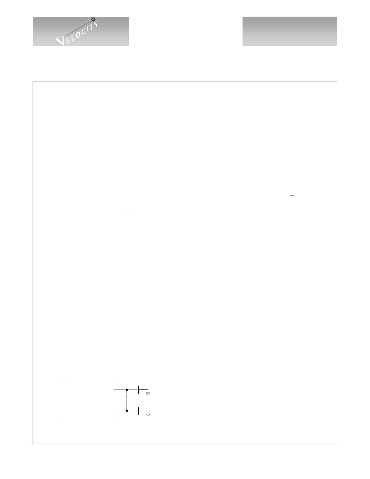
rate clock between 0.98GHz and 1.36GHz. The on-chip PLL uses a single external 0.1µF capacitor, connected
between CAP0 and CAP1, to control the Loop Filter. This capacitor should be a multilayer ceramic dielectric,
or better, with at least a 5V working voltage rating and a good temperature coefficient (NPO is preferred but
X7R may be acceptable). These capacitors are used to minimiz e the impact of comm on-mode noise o n the
Clock Multiplier Unit, especially power supply noise . Higher value cap acitors provide better robu stness in
systems. NPO is preferred because if an X7R capacitor is used, the power supply noise sensitivity will vary
with temperature. For best noise immunity, the designer may use a three capacitor circuit with one differential
capacitor between CAP0 and CAP1, C1, a capacitor from CAP0 to ground, C2, and a capacitor from CAP1 to
ground, C3. Larger val ues are b etter bu t 0.1µF is adequat e. However, if the designer cannot use a thre e capacit or
circuit, a single differential capacitor, C1, is adequate. These components should be isolated from noisy traces.
Figure 1: Loop Filter Capacitors (best circuit)
C1=C2=C3= >0.1µF
MultiLayer Ceramic
Surface Mount
NPO (Preferred) or X7R
5V Working Voltage Rating
CAP0
VSC7216-01
CAP1
C2
C1
C3
Page 2 G52352-0, Rev 3.2
© VITESSE SEMICONDUCTOR CORPORATION • 741 Calle Plano • Camarillo, CA 93012
Tel: (800) VITESSE • FAX: (805) 987-5896 • Email: prodinfo@vitesse.com
Internet: www.vitesse.com
05/05/01
Preliminary Datasheet
VITESSE
SEMICONDUCTOR CORPORATION
VSC7216-01
The REFCLK signal can be either single-ended TTL or differential LVPECL. If TTL, connect the TTL
input to REFCLKP but leave REFCLKN open. If LVPECL, connect the inputs to REFCLKP and REFCLKN.
Internal biasing resistors sets the proper DC level to V
Serial and parallel data rates for all channels may be halved by means of the RATE pin. When RATE is
HIGH, the chip is in full-speed mode (default mode of operation) and when LOW, the half-speed mode is
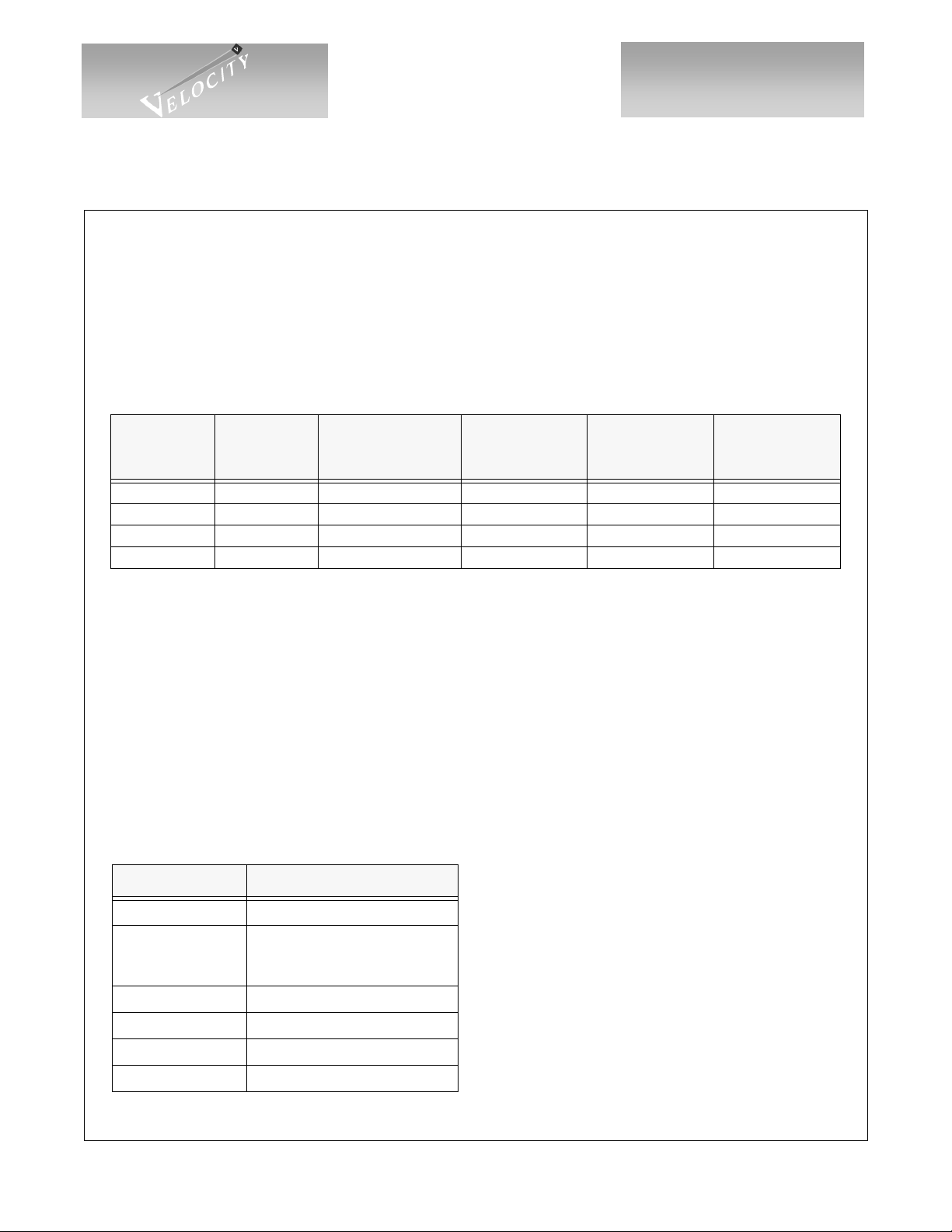
selected. Table 1 shows the interaction of the DUAL and RATE inputs.
Table 1: Using the RATE input to Achieve Half-Speed Operation
Clock
RATE Pin DUAL Pin
0 0 x10 500Mb/s 50Mb/s 50MHz
0 1 x20 500Mb/s 50Mb/s 25MHz
1 0 x10 1Gb/s 100Mb/s 100MHz
1 1 x20 1Gb/s 100Mb/s 50MHz
Multiplication
Factor
/2.
DD
Serial Link
Speed
Multi-Gigabit Interconnect Chip
Parallel
Data Rate
REFCLK
Frequency
Transmitter Functional Description
Transmitter Data Bus
Each VSC7216-01 transmit channel has an 8-bit input transmit data character, Tn(7:0), and two control
inputs, C/Dn and WSENn. The C/Dn input determines whether a norm al data character or a special “K-
character” is transmitted, and the WSENn input initiates transmission of a 16-character “Word Sync Sequence”
used to align the receive channels. These data and control inputs are clocked either on the rising edge of
REFCLK, on the rising edge of TB Cn , or wit hi n t he data ey e for med by T BCn. W hen n ot usin g REFC LK, each
channel uses either its own TBCn input, or uses the TBCA input. The transmit interface mode is controlled by
TMODE(2:0) as shown in Table 2.
Table 2: Transmit Interface Input Timing Mode
TMODE(2:0) Input Timing Reference
0 0 0 REFCLK Rising Edge
0 0 1
0 1 0
0 1 1
1 0 0 TBCA Rising Edge
1 0 1 TBCn Rising Edge
1 1 0 TBCA Data Eye
1 1 1 TBCn Data Eye
G52352-0, Rev 3.2 Page 3
05/05/01
© VITESSE SEMICONDUCTOR CORPORATION • 741 C al l e P lan o • Camarillo, CA 93012
Reserved
Tel: (800) VITESSE • FAX: (805) 987-5896 • Email: prodinfo@vitesse.com
Internet: www.vitesse.com
VITESSE
SEMICONDUCTOR CORPORATION
Multi-Gigabit Interconnect Chip
Multi-Gigabit Interconnect Chip
When used, the TBCn inputs must be frequency-locked to REFCLK. No phase relationship is assumed. A
small skew buffer is provided to tolerate phase drift between TBCn and REFCLK. This buffer is recentered by
the RESETN input, and the total phase drift after recentering must be limited to ±180
character time). Each channel has an error output, TBERRn, that is asserted HIGH to indicate that the phase
drift between TBCn and REFCLK has accumulated to the point that the e lastic limit of the skew buffer has been
exceeded and a transmit data character has been either dropped or duplicated. This error can not occur when
input timing is referenced to REF CLK. The TBERRn output tim ing is identical to the low-spe ed receiver
outputs, as selected by RMODE(1:0) in Table 6.
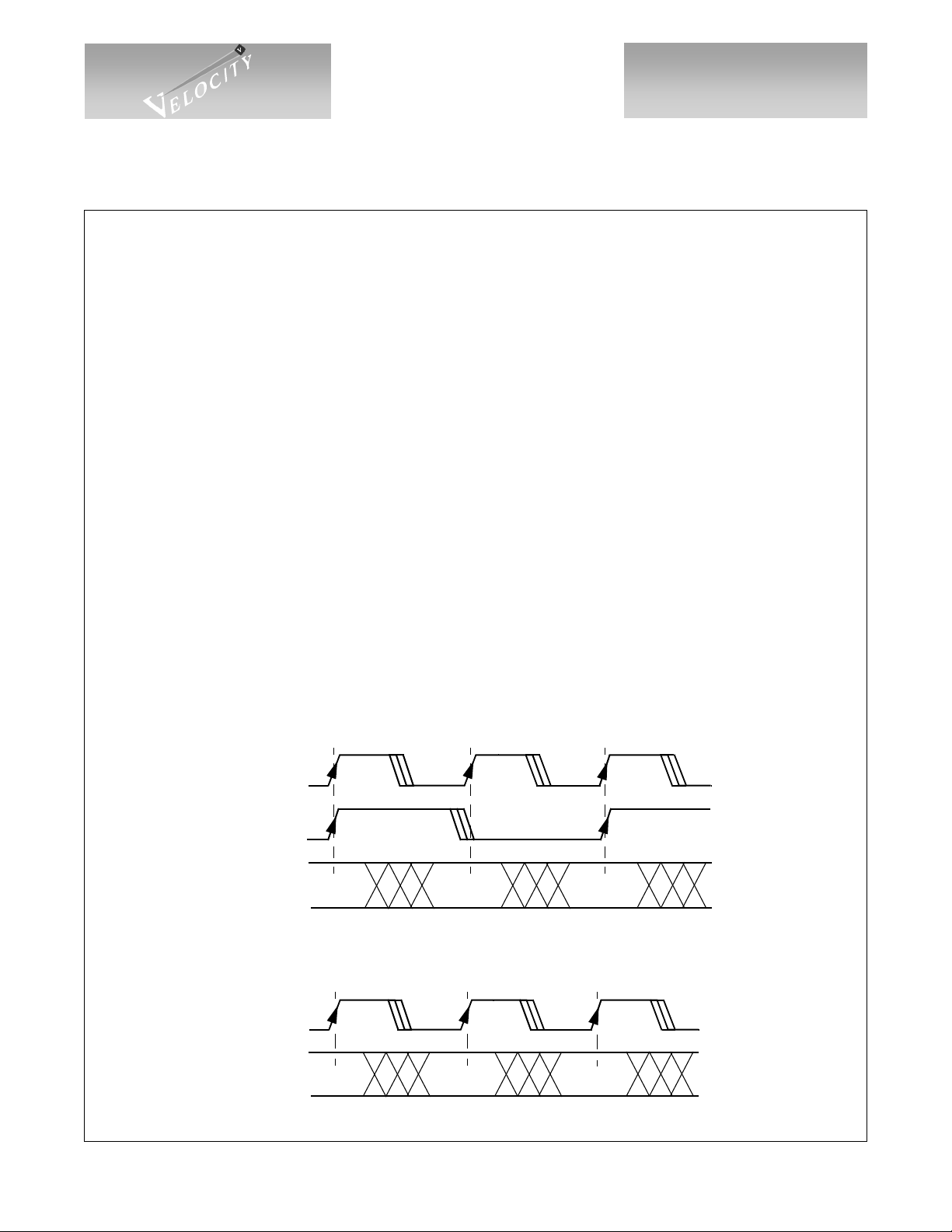
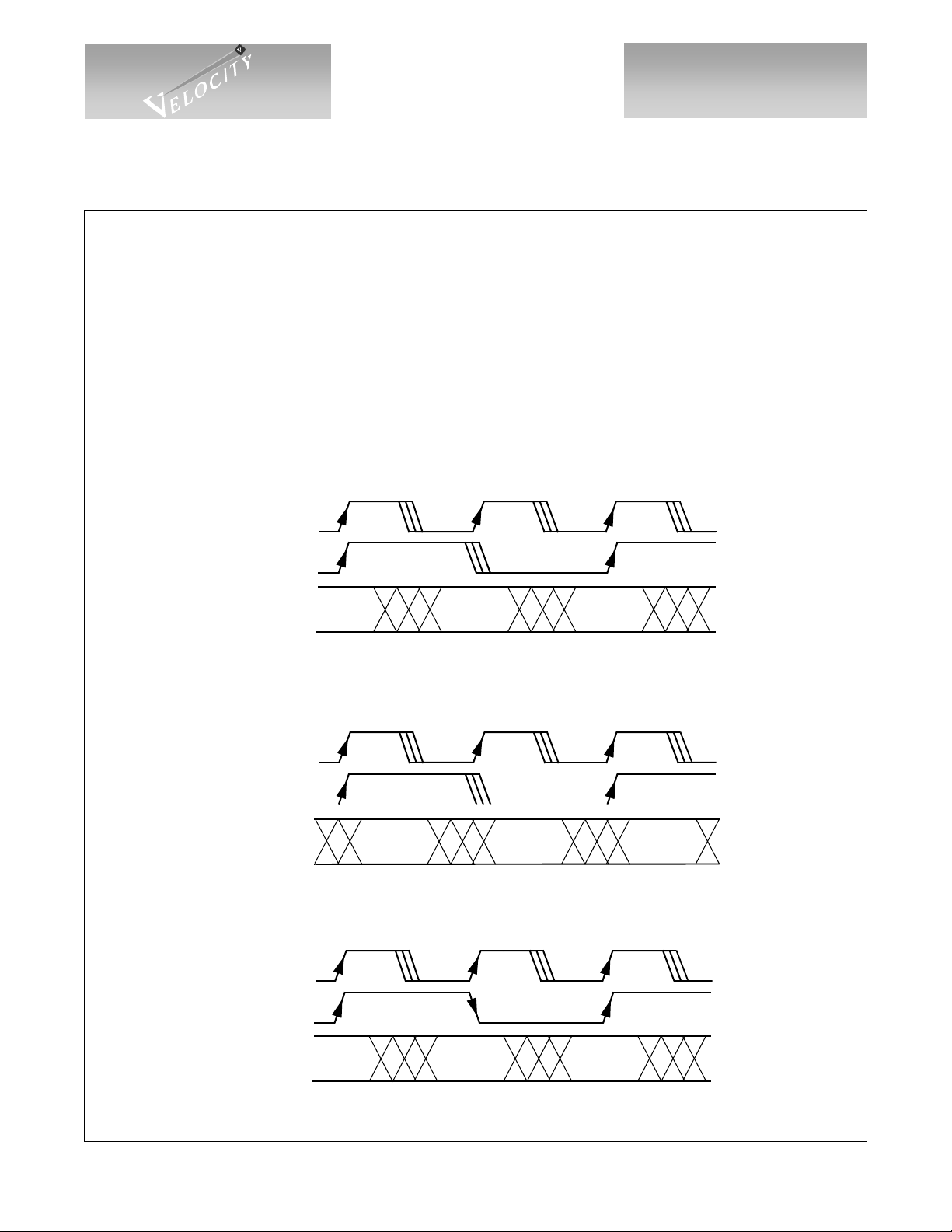
Figures 2 through 4 show the possible relationships between data and control inputs and the selected input
timing source. Figure 2 shows how REFC LK is used as an input timing refe rence. This m ode of opera tion is
used in the VSC7211 and VSC7214. Figure 3 and Figure 4 show how TBCn is used as an input timing
reference. When TBCn is used to define a data eye as shown in Figu re 4, it functions as an additional data input
that simply toggles every cycle.
Note that the REFCLK and TBCn inputs are n ot used directly t o clock th e input dat a. Instea d, an int ernal
Phase-Lock Loop (PLL) generates edges aligned with the appropriate clock. The arrows on the rising edges of
these signals define the reference edge for the internal phase detection logic. An internal clock is generated at
one-tenth the serial transmit data rate that is lock ed to the selected input tim ing source. This is an especially
important issue when DUAL is HIGH and input timing is referenced to REFCLK, since the falling edge is NOT
used. The internal clock active edges are placed co incident with the REFCLK rising ed ges and halfway bet ween
the REFCLK rising edges in this mode.
A similar situation exists when TBCn is used to define a data eye, only the risi ng edges of TBCn are used to
define the externa l data timing. The internal cloc k active edges are placed at 90
consecutive TBCn rising edges (which are assumed to be 360
° apart).
Preliminary Data Sheet
VSC7216-01
° (where 360 ° is one
° and 270° points between
VSC7216
Figure 2: Transmit Timing, TMODE(2:0) = 000
REFCLK
(DUAL = 0)
REFCLK
(DUAL = 1
Tn(7:0)
C/Dn
WSENn
TBCA
TBCn
Tn(7:0)
WSENn
Page 4 G52352-0, Rev 3.2
)
Valid
Figure 3: Transmit Timing, TMODE(2:0) = 10X
or
C/Dn
© VITESSE SEMICONDUCTOR CORPORATION • 741 Calle Plano • Camarillo, CA 93012
Valid
Tel: (800) VITESSE • FAX: (805) 987-5896 • Email: prodinfo@vitesse.com
Valid Valid
Valid Val i d
Internet: www.vitesse.com
05/05/01
Preliminary Datasheet
VITESSE
SEMICONDUCTOR CORPORATION
VSC7216-01
Multi-Gigabit Interconnect Chip
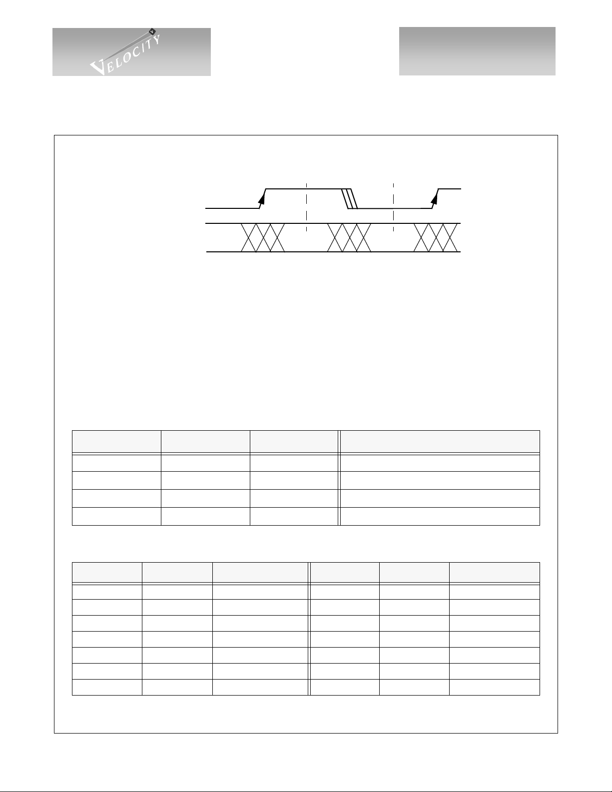
Figure 4: Transmit Timing, TMODE(2:0) = 11X (“ASIC-Friendly” Timing)
TBCA
or
TBCn
Tn(7:0)
C/Dn
WSENn
V alid
o
0
o
90
Valid Valid
180
o
270
o
360
o
8B/10B Encoder
Each channel contains an 8B/10B encoder which translates the 8-bit input data on Tn(7:0) into a 10-bit
encoded data character. C/Dn inputs are also provided in each channel which, along with KCHAR, allow the
transmission of special Fibre Channel Kxx. x characters (see Table 3). Note that KCHAR is a static input, and
does NOT have the same input timing as Tn (7:0), C/Dn and WSENn. Normally C/Dn is LOW in order to
transmit data. If C/Dn is HIGH and KCHAR is LOW, then a Fibre Channel defined IDLE Character (K28.5 =
‘0011111010’ or ‘1100000101’ depending on disparity) is transmitted and Tn(7:0) is ignored. If C/Dn is HIGH
and KCHAR is HIGH, a Kxx.x character is transmitted as determined by the data pattern on Tn(7:0) (see Table
4). Data patterns other than those defined in Table 4 produce undefined 10B encodings.
Table 3: Transmit Data Controls
WSENn C/Dn KCHAR Encoded 10-Bit Output
0 0 X Data Character
0 1 0 IDLE Character (K28.5)
0 1 1 Special Kxx.x Character
1 X X 16-Character Word Sync Sequence
Table 4: Special Characters (Selected when C/Dn and KCHAR are HIGH)
Code Tn(7:0) Comment Code Tn(7:0) Comment
K28.0 000 11100 User Defined K28.5- 101 01101 User Defined
K28.1 001 11100
K28.2 010 11100
K28.3 011 11100
K28.4 100 11100
K28.5 101 11100
K28.5+ 101 01100
User Defined K28.6 110 11100 User Defined
User Defined K28.7 111 11100 Test Only
User Defined K23.7 111 10111 User Defined
User Defined K27.7 111 11011 User Defined
IDLE K29.7 111 11101 User Defined
User Defined K30.7 111 11110 User Defined
G52352-0, Rev 3.2 Page 5
05/05/01
© VITESSE SEMICONDUCTOR CORPORATION • 741 C al l e P lan o • Camarillo, CA 93012
Tel: (800) VITESSE • FAX: (805) 987-5896 • Email: prodinfo@vitesse.com
Internet: www.vitesse.com
VITESSE
SEMICONDUCTOR CORPORATION
Multi-Gigabit Interconnect Chip
Multi-Gigabit Interconnect Chip
Encoder Bypass Mode
When ENDEC is LOW, the 8B/10B encoders are bypassed and a 10-bit input character Tn(7:0) is serialized
directly in each channel, bit Tn0 is transmitted first. The C/Dn input becomes Tn8, and WSENn becomes Tn9.
The KCHAR input becomes EN CDET which is not used in the transm itter, but when HIGH, enables Com ma
detection in all four recei vers. Ref er to the D ecoder Bypass Mode section for a description of this mode of
operation in the receiver. The latency through the transmitter is reduced by one character time when ENDEC is
LOW. This mode of opera tio n is si milar to a 10 -b it in terfa ce c omm only f oun d in seri alize r/d ese riali zers for th e
Fibre Channel ( VSC7125) and Gigabit Ethernet markets (VSC7135).
Word Sync Generation
The VSC7216-01 can perform channe l alignment (also referr ed to as “word alignment” or “word sync”),
meaning that the four rece ive data o utput stream s are aligned su ch that the s ame 4-byte word pres ented to t he
four transmit channel inpu ts for serialization will be transferred on the receive ch annel parallel ou tputs. The
Word Sync Sequence provides a unique synchronization point in the serial data stream that is used to align the
receive channels. This sequence consists of 16 consecutive K28.5 IDLE char acters with dispari ty reversals on
the second and fourth characters. The Word Sync Sequence is sent either as “I+ I+ I- I- I+ I- I+ I- I+ I- I+ I- I+
I- I+ I-” or as “I- I- I+ I+ I- I+ I- I+ I- I+ I- I+ I- I+ I- I+”, depending on the transmitter’s running disparity at the
time the first IDLE character is serialized.
Transmission of the Word Sync Sequence is initiated independently in each channel when the WSENn
input is asserted HIGH for one character time (see Figure 5). When WSENn is HIGH, the C/Dn and Tn(7:0)
inputs are ignored. The WSENn, C/Dn and Tn(7:0) inputs are also ignored f or the subsequent 15 character
times. In Figure 5, the Word Sync Sequence is initiated in cycle W1 and transmitted through cycle W16.
Normal data transmission (or the transmission of another Word Sync Sequence) resumes in cycle D3. This
figure is illustrated assuming that input timing is referenced to REFCLK (e.g., TMODE(2:0)=000) with the
DUAL input LOW. As long as WSENn remains asserted, another Word Sync Sequence will be generated.
Preliminary Data Sheet
VSC7216-01
VSC7216
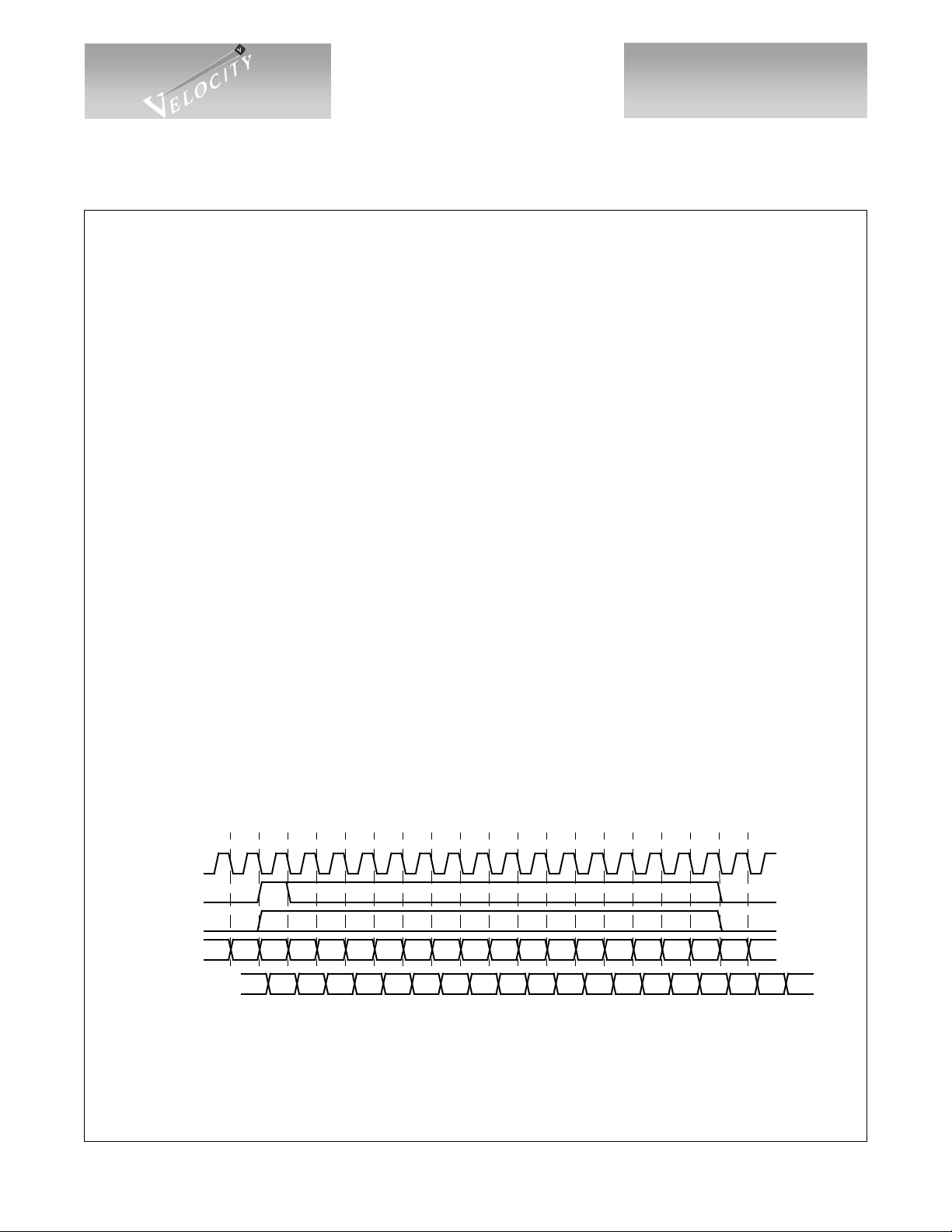
Figure 5: Word Sync Sequence Generation
D2D1 W2W1 W4W3 W6W5 W8W7 W10W9 W12W11 W14W13 W16W15 D4D3
REFCLK
WSENn
C/Dn
Tn(7:0)
TXn+/-
Page 6 G52352-0, Rev 3.2
0x020x01 XXXX XXXX XXXX XXXX XXXX XXXX XXXX XXXX 0x040x03
D2.0+D1.0+ K28.5+K28.5+ K28.5-K28.5- K28.5-K28.5+ K28.5-K28.5+ K28.5-K28.5+ K28.5-K28.5+ K28.5-K28.5+ K28.5-K28.5+ D4.0-D3.0+
© VITESSE SEMICONDUCTOR CORPORATION • 741 Calle Plano • Camarillo, CA 93012
Tel: (800) VITESSE • FAX: (805) 987-5896 • Email: prodinfo@vitesse.com
Internet: www.vitesse.com
05/05/01
Preliminary Datasheet
VITESSE
SEMICONDUCTOR CORPORATION
VSC7216-01
Serializer
The 10-bit output from the encoder (or from the encoder input register if ENDEC is LOW) is fed into a
multiplexer which serializes the parallel data using the synthesized transmit clock. The least significant bit of
the 10B data is transmitted first. Each channel has both primary and redundant serial output ports, PTXn and
RTXn respectively, which consist of differential PECL output buffers operating at either 10 or 20 times the
REFCLK rate. The primary and redundant transmitter outputs are separately controllable on each channel. The
primary PECL outputs PTXn are enabled when the PTXENn input is HIGH, and the redundant PECL outputs
RTXn are enabled when the RTXENn input is HIGH. Whe n a PEC L out put is dis abled, the ass ociated out put
buffers do not consume power and the atta ched pins are un-driven. The PECL outputs do not require externa l
resistors.
Multi-Gigabit Interconnect Chip
Receiver Functional Description
Serial Data Source
Each receive channel has both primary and redundant serial input ports, PRXn and RRXn, respectively,
which consist of differential PECL input buffers. Each channel also has a control input, RXP/Rn, used to select
either the primary or redundant serial input as the data source for that channel. When RXP/RC is HIGH, the C
channel serial data source is PRXC. When LBENn(1:0)=10, the channel’s transmitte r is looped ba ck and
becomes the serial data source regardless of the state of RXP/Rn (see Table 5).
T able 5: Serial Data Source Selection
LBENn(1:0) RXP/Rn Serial Data Source
≠ 1 0 0 RRXn
≠ 1 0 1 PRXn
= 1 0 X
Signal Detection
Each channel’s primary and redundant PECL input buffers have an associated signal detect output,
PSDETn and RSDETn. All eight outputs are available for continuous monitoring of both the selected and nonselected input. Each signal detect out put is asse rted HIGH when transit ions are detected on the associat ed PECL
input and the signal amplitude exceeds 200mV under nominal operating conditions. A LOW indicates that
either no transitions are detected or the signal amplitude is below 100mV under nominal operating conditions.
The signal detect out puts ar e considered undefined when the signal ampl it ud e i s in the 100mV to 200mV range.
The signal detect circuitry behaves like a re-triggerable one-shot that is triggered by signal transitions, and
whose time-out interval ranges from 40 to 80 bit t i mes. T he t r ansi ti on de nsit y i s no t checked to make sure that it
Loopback fromTransmitters
LBTXn
G52352-0, Rev 3.2 Page 7
05/05/01
© VITESSE SEMICONDUCTOR CORPORATION • 741 C al l e P lan o • Camarillo, CA 93012
Tel: (800) VITESSE • FAX: (805) 987-5896 • Email: prodinfo@vitesse.com
Internet: www.vitesse.com

VITESSE
SEMICONDUCTOR CORPORATION
Multi-Gigabit Interconnect Chip
Multi-Gigabit Interconnect Chip
corresponds to a valid Fibre Channel data stream. The PSDETn and RSDETn output timing is identical to the
low-speed receiver outputs, as selected by RMODE(1:0). See Table 6.
Receiver Equalization
Incoming data on the PR X/RRX inp uts typ ically co ntain s a subst antia l amount of Int er Sy mbol Inte rfere nce
(ISI) or deterministic jitter which reduces the ability of the receiver to recover data without errors. An equalizer
has been added to each of the recei ver ’s input buffers in order to compensate for this deterministic jitter. This
circuit has been designed to effectively reduce the ISI commonly found in copper c ables or backplane t races due
to low frequencies traveling faster than high frequencies as a result of the skin effect. The equalizer boosts high
frequency edge response in order to reduce the adverse effects of ISI.
Clock and Data Recovery
At the receiver, each channel contains an independent Clock Recovery Unit (CRU) which accepts the
selected serial input source, extracts the high-speed clock and retimes the data. Each CRU automatically locks
on data and if the data is not present, will automatically lock to the REFCLK. This maintains a very wellbehaved recovered clock, RCLKn/RCLKNn which does not contain any slivers and will operate at a frequency
of the REFCLK reference ±200 ppm. The use of an external Lock-to-Reference pin is not needed.
The Clock Recovery Unit must perform bit synchronization which occu rs when the CRU locks onto and
properly samples the incoming serial data as described in the previous paragraph. When the CRU is not locked
onto the serial data, the 10-bit data out of the decoder is invalid which results in numerous 8B/10B decoding
errors or disparity errors. When the link is disturbed (e.g., the cable is disconnected or the serial data source is
switched), the CRU will require a certain amount of time to lock onto data which is specified in the AC Timing
Characteristics for “Data Acquisition Lock Time.”
Preliminary Data Sheet
VSC7216-01
VSC7216
Deserializer and Character Alignment
The retimed serial data stream is converted into 10-bit characters by the deserializer. A special 7-bit
“Comma” pattern (‘0011111xxx’ or ‘1100000xxx’) is recognized by the receiver and allows it to identify the
10-bit character boundary. Note that this pattern is found in three special characters, K28.1, K28.5 and K28.7,
however, K28.5 is chosen as th e unique IDLE character. Only K28.1 and K2 8.5 should be us ed in normal
operation. The K28.7 character should be reserved for test and characterization use.
Character alignment occurs when the deserializer synchronizes the 10-bit character framing boundary to a
“Comma” pattern in the incoming serial data stream. If the receiver identifies a “Comma” pattern in the
incoming data stream which is misaligned to the current framing boundary the receiver will re-synchronize the
recovered data in order to align the data to the new “Comma” pattern. Re-synchronization ensures that the
“Comma” character is output on the internal 10-bit bus so that bits 0 through 9 equal ‘0011111xxx’ or
‘1100000xxx’. If the “Comma” pattern is aligned with the current framing boundary, re-synchronization will
not change the current alignment. Re-synchronization is always enabled and cann ot be turned of f when ENDEC
is HIGH. After character re-synchronization the VSC7216-01 ensures tha t within a link, the 8-bit data sent to
the transmitting VSC7216-01 will be recovered by the receiving VSC7216-01 in the same bit locations as the
transmitter (i.e., Tn(7:0) = Rn(7:0)). When ENDEC is LOW, “Comma” detection and alignment are enabled
only if KCHAR is HIGH.
Page 8 G52352-0, Rev 3.2
© VITESSE SEMICONDUCTOR CORPORATION • 741 Calle Plano • Camarillo, CA 93012
Tel: (800) VITESSE • FAX: (805) 987-5896 • Email: prodinfo@vitesse.com
Internet: www.vitesse.com
05/05/01
Preliminary Datasheet
VITESSE
SEMICONDUCTOR CORPORATION
VSC7216-01
10B/8B Decoder
The 10-bit character from the deseriali zer is dec oded in t he 10B/8B decod er, which outputs the 8B data byte
and three bits of status i nformat ion. If the 1 0-bit c haracter does not match a ny vali d valu e, an Out- of-Band Err or
is generated which is output on the receiver status bus. Similarly, if the running disparity of the character does
not match the expe cted va lue, a Disp arity Err or is gen erated. T he decode r also repo rts whe n a K-char acter is
received, and distinguishes the K28.5 (IDLE) cha racter from other K-char acters. This status information is
combined with LOS State Machine status and FIFO error status, to produce the prioritized per-character link
status output information (see Table 8).
Elastic Buffer and Channel De-Skewing
An elastic buffer is included in each of the four receive ch annels. D ecoded data and s tatus infor mation is
written into these buffers on each channel’s recovered clock, and is read on the selected output clock. In
addition to allowing decoded data to easily cross fro m a channel’s recovered clock domain to its output clock
domain, the elastic buffers facili ta te ch anne l alig nme nt (th e reco nstru ctio n o f a mult i-by te wor d as p res ented to
the transmitting devices), and they facilitate rate matching via IDLE character insertion/deletion when the
channel’s recovered clock is not frequency-locked to its output clock.
There are three conditions under which a receive channel’s elastic buffer is recentered: the RESETN input,
when asserted, recenters the read/write pointers in each elasticity buffer; whenever a “Comma” character is
received which changes the receive character’s framing boundary, the elasticity buffer is recentered; and lastly,
it is also recentered whenever the receiver detects the synchroniza tion point in the Word Sync Sequence. All
three of these events are associated with chip initialization or link initialization and would not occur during
normal data transfer. Note that recentering can result in the loss or duplication of decoded character data and
status information.
When a condition change transmit timing (e.g., phase shifts in TBC) or shifts phase/alignment into the
receiver, the user should initial a Word Sync Event to recenter all elasticity buffers. Otherwise, data corruption
could occur.
The VSC7216-01 presents recovered data on Rn(7:0) and status on IDLEn, KCHn and ERRn. These
outputs are timed either to each channel’s own recovered clock (RCLKn/RCLKNn), to Channel A’s recovered
clock (RCLKA/RCLKNA), or to REFCLK. The output timing reference is select ed by RMODE(1:0) (see Table
6). The transmitter input skew buffer error outputs TBERRn and the analog signal detect outputs PSDETn and
RSDETn are also synchronized to the selected output timing reference. There are two choices for REFCLKbased timing, which differ in the positioning of the data valid window associated with the output signals timed
to REFCLK: when RMODE(1:0)=00 REFCLK is approximately centered in the output data valid window as in
the VSC7214 and when RMODE(1:0)=01 REFCLK slightly leads the data valid window so that output data
appears to have a more typical “Clock-to-Q” timing relationship to REFCLK.
Multi-Gigabit Interconnect Chip
T able 6: Receive Interface Output Timing Mode
RMODE(1:0) Output Timing Reference
0 0 REFCLK (centered)
0 1 REFCLK (leading)
1 0 RCLKA/RCLKNA
1 1 RCLKn/RCLKNn
G52352-0, Rev 3.2 Page 9
05/05/01
© VITESSE SEMICONDUCTOR CORPORATION • 741 C al l e P lan o • Camarillo, CA 93012
Tel: (800) VITESSE • FAX: (805) 987-5896 • Email: prodinfo@vitesse.com
Internet: www.vitesse.com
VITESSE
SEMICONDUCTOR CORPORATION
Multi-Gigabit Interconnect Chip
Multi-Gigabit Interconnect Chip
Preliminary Data Sheet
VSC7216-01
VSC7216
The term “wo rd clock” will be used for whichever clock, REFCLK, RCLKA/RCLKNA or RCLKn/
RCLKNn, is selected as the output timing reference. If RMODE(1) is HIGH, each channels’ RCLKn/RCLKNn
outputs are complementary outputs at 1/ 10th or 1/20th the baud rate of the incomi ng data depending upon
DUAL. When RCLKA/RCLKNA is selected as the output t iming reference, the Channel B, C and D RCLKn/
RCLKNn outputs are copies of RCLKA/RCLKNA. If RMOD E(1) is LOW, then each channels’ RCLKn/
RCLKNn outputs are held in a LOW/HIGH state, respectively, and the data and status outputs are timed to
REFCLK. If DUAL is HIGH, all d ata at the four output po rts are s ynchronously clock ed out on both positive
and negative edges of the selected word clock at 1/20th the baud rate. If DUAL is LOW, the data is clocked out
of the VSC7216-01 only on the rising edge of the selected word clock at 1/10th the baud rate. Timing
waveforms for the output data and status are shown in Figure 6, Figure 7 and Figure 8.
Figure 6: Receive Timing, RMODE(1:0) = 00
REFCLK
(DUAL = 0)
REFCLK
(DUAL = 1)
Rn(7:0)
IDLEn
KCHn
ERRn
V alid
Valid Val i d
REFCLK
(DUAL = 0)
REFCLK
(DUAL = 1)
Rn(7:0)
IDLEn
KCHn
ERRn
RCLKn
(DUAL = 0)
RCLKn
(DUAL = 1)
Rn(7:0)
IDLEn
KCHn
ERRn
Figure 7: Receive Timing, RMODE(1:0) = 01
Valid
Figure 8: Receive Timing, RMODE(1:0) = 1X
Valid
V alid Valid
Vali d Val i d
Page 10 G52352-0, Rev 3.2
© VITESSE SEMICONDUCTOR CORPORATION • 741 Calle Plano • Camarillo, CA 93012
Tel: (800) VITESSE • FAX: (805) 987-5896 • Email: prodinfo@vitesse.com
Internet: www.vitesse.com
05/05/01

Preliminary Datasheet
VITESSE
SEMICONDUCTOR CORPORATION
VSC7216-01
The data coming from the decoder is clocked into the elastic buffer by the recovered clock from the
channel’s CRU. The data is clocked out of the elastic buffers with word clock. If the transmitting device’s
REFCLK is not precisely frequency-locked to a receive channel’s word clock, the channel’s elastic buffer will
tend to gradually fill or empty as the recovered clock (which is by definition frequency-locked to the
transmitter’s REFCLK) steadily drifts in phase relative to the word c lock.
In order to accommodate frequency differences betwee n a transmitter’s REFCLK and the word clock, the
VSC7216-01 can automatically perform rate matching by either deleting or duplicating IDLE character s. The
FLOCK input must be LOW to enable rate matching which, based on how the WSI input is connected, can
either be performed in each channel individually or can be performed in parallel across a group of channels that
are word-aligned. This is discussed in detail in the Word Alignment section below. It is the user ’s responsibility
to ensure that the frequency at which IDLEs are simultaneously transmitted on each channel accommodates the
frequency differences, if any, in their system architecture. Not meeting the IDLE density requirements could
result in Underrun/Overrun Errors. Howe ver, the use of a continuous stream of I DLE characters should be
avoided when rate matching i s enable. The IDLE addition/deletion l ogi c r el i es on th e st atu s bi ts (s ee Table 8 for
details) to identify K28.5 IDLE characters. The use of continuous IDLE characters will force the VSC7216-01
into the RESYNC state (see Figure 9) resulting in a status bit sequence which the addition/deletion logic does
not recognize as an IDLE character.
The elastic buffer is designed to allow a maximum phase drift of +2 or -2 serial clock bit times between resynchronizations, which sets a limit on the maximum data “packet” length allowed between IDLEs. This
maximum packet length depends on the frequency difference between the transmitting and receiving device’s
REFCLKs. Let represent phase drift in bit times, and let represent one full 10-bit character of phase
drift. Limiting phase drift to two bit times means the following inequality must be satisfied :
∆φ 2π
Multi-Gigabit Interconnect Chip
(1)
Let L be the number o f 10-bit characters transmitted, and let
phase drift in bit times is given by:
(2)
A simple expression for maximum packet len gt h as a fun c tion of frequency offset is derive d by su bst itut ing
(2) in (1) and solving for L:
(3)
As an example, if the frequency offset is 200ppm, the maximum packet length should not be more than 1K
bytes. To increase the maximum packet length L, decrease the frequency offset
K28.5 is transmitted between “packets” of data, it might be dropped during compensation for phase drift. If the
user must have at least one K28.5 between these two packets, then two K28.5s must be transmitted.
Word Alignment
The VSC7216-01 performs channel-to-channel word alignment. In this mode of operation, if the data from
all four channels on the transmitting VSC7216-01 (e.g., the 4 Tn(7:0) busses) is viewed as a 32-bit word, then
the receiving VSC7216-01 will recover an identical word. For example, if a transmit pattern was ‘ABCD’,
G52352-0, Rev 3.2 Page 11
05/05/01
© VITESSE SEMICONDUCTOR CORPORATION • 741 C al l e P lan o • Camarillo, CA 93012
Tel: (800) VITESSE • FAX: (805) 987-5896 • Email: prodinfo@vitesse.com
∆φ 0.2 2π×()≤
∆φ ∆
L 0.2 10
f 10
⁄()2π× L=
×()∆f⁄≤
Internet: www.vitesse.com
∆f be the frequ ency o ffset in ppm. T he tot al
6
6
∆f. Please note that if only one
VITESSE
SEMICONDUCTOR CORPORATION
Multi-Gigabit Interconnect Chip
Multi-Gigabit Interconnect Chip
‘EFGH’, ‘IJKL’, etc., the receiver shoul d not recover data words as ‘ABGD’, ‘EFKH’, ‘IJOL’, etc. This requires
the four transmit channels to o btain input data on a common cl ock (e.g., TMODE(2: 0)=000 or 1X0) and th e
four receive channels to present output data on a common word clock (e.g., RMODE(1:0)=0X or 10).
Within the receiver there are elastic buffers used to deskew the four channels and align them to a common
word clock. An elastic buff er all ows the channels’ input to be skewed up to ±6 bit times (1 2 bi t times t ot al skew
between any two channels) in order to accommoda te circuit imperfections, differences in tran smission delay
and jitter. Multiple VSC7216-01 devices can also be used in synchronous operation if the skew between all
serial input pairs is maintained less than ±6 serial clock bit times. This allows easy implementation of robust
systems, and is discussed in greater detail in the Using Multiple VSC7216-01s in Parallel section.
In order to perform wo rd alignment, a synchr onization point must be se en across all aligned r eceive
channels within the +/-6 bit time window. The VSC7216-01 receiver recognizes the first four characters of the
Word Sync Sequence (either K28.5+ K28.5+ K28.5- K28.5- or K28.5- K 28.5- K28.5+ K28.5+) as the
synchronization point. As a model for understanding, consider the case where a VSC7216-01 transmitter sends
32 bits of data to the receiver via copper media which has small cable length differences causing a channel-tochannel skew. All transmit channels that are to be word aligned transmit the Word Sync Sequence in parallel.
On detection of the synchronization point, the receivers will reposition the recovered da ta within their elastic
buffers in order to align all four channels and remove any channel-to-channel skew. All normal data characters
following the Word Sync Sequence will be properly word aligned. In the process of channel alignment, one or
two of the final twelve K28.5 characters in the Word Sync Sequence may be deleted or duplicated. This ensures
that each transmitted 32 -bit word is recovered correctly.
The VSC7216-01 is capable of performing rate matc hing in word-aligned application s by inserting or
deleting IDLEs in parallel across the aligned receive channels. This requires that the word-aligned data streams
contain IDLEs inserted in parallel on all transmit channels (e.g., an IDLE “word”) according to the IDLE
density requirement previously described.
Word alignment is enabled by connecting the WSI input to a WSO output, either from the same device if a
single device is used, or from another device if multiple devices are used in parallel to align more than four
channels. The FLOCK inp ut sta te and WSI input source determine whet her or not r at e mat chi ng ( ID LE del et i on
or duplication) will be performed, and whether it is done independently on each channel or in parallel across
aligned channels. Word alignment is disabled when WSI is not connected to a WSO output. Rate matching is
disabled when either FLOCK is HIGH or WSI is held LOW (see Table 7).
Preliminary Data Sheet
VSC7216-01
VSC7216
Table 7: Word Alignment and Rate Matching Control
FLOCK WSI Source Word Alignment Rate Matching
0 0 Off Off
0 1 Off Enabled, Independent Cha n ne ls
0 WSO Enabled Enabled, Aligned Channels
1 0 Off Off
1 1 Off Off
1 WSO Enabled Off
Page 12 G52352-0, Rev 3.2
© VITESSE SEMICONDUCTOR CORPORATION • 741 Calle Plano • Camarillo, CA 93012
Tel: (800) VITESSE • FAX: (805) 987-5896 • Email: prodinfo@vitesse.com
Internet: www.vitesse.com
05/05/01
 Loading...