

VITESSE VSC7212RG Datasheet

Preliminary Data Sheet
VITESSE
VITESSE
SEMICONDUCTOR CORPORATION
SEMICONDUCTOR CORPORATION
VSC7212
Gigabit Interconnect Chip
Features
• ANSI X3T11 Compliant Fibre Channel and IEEE
802.3z Compliant Gigabit Ethernet Transceiver
• Over 2Gb/s Duplex Raw Data Rate
• Redundant PECL Tx Outputs and Rx Inputs
• 8B/10B Encoder/Decoder, Optional Encoder/
Decoder Bypass Operation
• “ASIC-Friendly
TM
” Timing Options fo r Transmit-
ter Parallel Input Data
• Elastic Buffer for Chip-to-Chip Cable Deskewing
• Tx/Rx Rate Matching via IDLE Insertion/Deletion
• Compatible with VSC7211, VSC7214 and
VSC7216
• Received Data Aligned to Local REFCLK or to
Recovered Clock
• PECL Rx Signal Detect and Cable Equalization
• Serial Tx-to-Rx and Parallel Rx-to-Tx Internal
Loopback Modes
• Clock Multiplier Generates Baud Rate Clock
• Automatic Lock-to-Reference
• JTAG Boundary Scan Support for TTL I/O
• Built-In Self Test
• 3.3V Supply, 1.0 W
• 100-pin, 14mm TQFP package
General Description
The VSC7212 is an 8-bit parallel-to-serial and serial-to-parallel transceiver chip used for high bandwidth
interconnection between busses, backplanes, or other subsystems. A Fibre Channel and Gigabit Ethernet
compliant transceiv er provides up to 2. 18Gb/s of duplex raw data transf er. The VSC7212 can operat e at a
maximum data transfer rate of 1088Mb/s (8 bits at 136MHz) or a minimum rate of 784Mb/s (8 bits at 98MHz).
The VSC7212 contains an 8B/10B encoder, serializer, de-serializer, 8B/10B decoder and elastic buffer which
provide the user with a simple interface for transferring data serially and recovering it on the receive side. The
device can also be configured to operate as a non-encoded 10-bit transceiver with redundant I/O.
VSC7212 Block Diagram
TRANSMITTER
PTXEN
8B/10B
Encode
© VITESSE SEMICONDUCTOR CORPORATION • 741 Calle Plano • Camarillo, CA 93012
10
RTXEN
Tx Clock
REFCLK
TBERR
REFOUT
Tel: (800)-VITESSE • FAX: (805) 987-5896 • Email: prodinfo@vitesse.com
C/D
TBC
88
DQ
x20/x10
Clock Gen
CAP0 CAP1
T(7:0)
WSEN
KCHAR
DUAL
REFCLKP
REFCLKN
G52268-0, Rev 3.3 Page 1
04/10/01
LBTX
LBEN(1:0)
RXP/R
PTX+
PRX+
PTX-
PRX-
RTX+
RRX+
RTX-
RRX-
TMODE(2:0)
RMODE(1:0)
Internet: www.vitesse.com
RECEIVER
Clk/Data
Recovery
PSDET
RSDET
RESETN
ENDEC
BIST
10
8B/10B
Decode
FLOCK
TRSTN
WSI
TMS
TDI
TCK
8
3
Elastic
Buffer
Channel
Align
JTAG
Boundary
Scan
8
R(7:0)
IDLE
KCH
ERR
RCLK
RCLKN
WSO
TDO
VITESSE
SEMICONDUCTOR CORPORATION
SEMICONDUCTOR CORPORATION
ESE
Preliminary Data Sheet
Gigabit Interconnect Chip
Notation
Differential signals (i.e., PTX+ and PTX-) may be referred to as a single signal (i.e., PTX) by dropping
reference to the “+” and “- ”. REFCLK refers to the single-ended TTL or differential PECL input pair
REFCLKP/REFCLKN, whichever is used.
Clock Synthesizer
Depending on the state of the DUAL input, the V SC7212 clock synthesizer m ultiplies the reference
frequency provided on the REFCLK inp ut by 10 (DUAL is LOW) or 20 ( DUAL is HIGH) to achie ve a baud
rate clock between 0.98GHz and 1.36GHz. The on-chip PLL uses a single external 0.1µF capacitor, connected
between CAP0 and CAP1, to control the Loop Filter. This capacitor should be a multilayer ceramic dielectric,
or better, with at least a 5V working voltage rating and a good temperature coefficient; NPO is preferred but
X7R may be acceptable. These capacitors are used to minimize the impact of common-mode noise on the Clock
Multiplier Unit, especially power supply noise. Higher value capacitors provide better robustness in systems.
NPO is preferred because if an X7R capacitor is used, the powe r supply noise sensitivity w ill vary with
temperature. For best noise immunity, the designer may use a three capacitor circuit with one differential
capacitor between CAP0 and CAP1, C1, a capacitor from CAP0 to ground, C2, and a capacitor from CAP1 to
ground, C3. Larger val ues are b etter bu t 0.1µF is adequat e. However, if the designe r canno t use a th ree capac itor
circuit, a single differential capacitor, C1, is adequate. These components should be isolated from noisy traces.
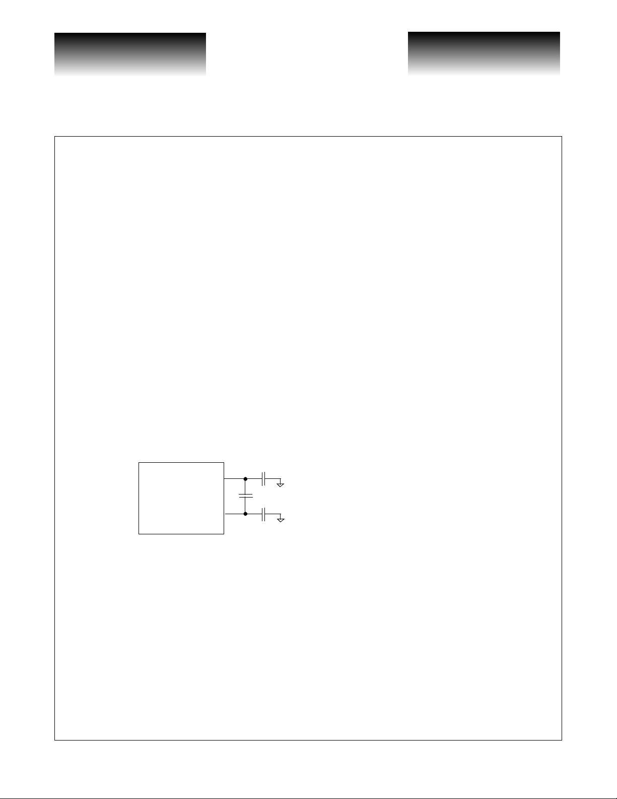
Figure 1: Loop Filter Capacitors (Best Circuit)
VSC7212
CAP0
VSC7216
CAP1
The REFCLK signal can be either single-ended TTL or differential LVPECL. If TTL, connect the TTL
input to REFCLKP but leave REFCLKN open. If LVPECL, connect the inputs to REFCLKP and REFCLKN.
Internal biasing resistors sets the proper DC Leve l to V
Page 2 G52268-0, Rev 3.3
© VITESSE SEMICONDUCTOR CORPORATION • 741 Calle Plano • Camarillo, CA 93012
Tel: (800)-VITESSE • FAX: (805) 987-5896 • Email: prodinfo@vitesse.com
C1
C2
C3
/2.
DD
Internet: www.vitesse.com
C1=C2=C3= >0.1µF
MultiLayer Ceramic
Surface Mount
NPO (Preferred) or X7R
5V Working Voltage Rating
04/10/01
Preliminary Data Sheet
VITESSE
VITESSE
SEMICONDUCTOR CORPORATION
SEMICONDUCTOR CORPORATION
VSC7212
Gigabit Interconnect Chip
Transmitter Functional Description
Transmitter Data Bus
The VSC7212 transmitter has an 8-bit input transmit data character, T(7:0), and two control inputs, C/D and
WSEN. The C/D input determines whether a normal data character or a special “K-character ” is transmitted,
and the WSEN input ini tiates tr ansmissio n of a 16-ch aracter “Word Sync Sequence” used to align the receiver.
These data and control inputs are clocked either on the rising edge of REFCLK, on the rising edge of TBC, or
within the data eye forme d by TBC ( “ASIC-Friendly” timing). The transmit interfa ce mode is con trolled by
TMODE(2:0) as shown in Table 1.
When used, TBC must be frequency locked to REFCLK. No phase relationship is assumed. A small skew
buffer is provided to tolerate phase drift between TBC and REFCLK. This buffer is recentered by the RESETN
input, and the total ph ase drift after recenteri ng must be limited to +/- 180× (where 360× is one character time).
The VSC7212 has an error output, TBERR, that is asserted HIGH to indicate that the phase drift between TBC
and REFCLK has accumulated to the point that the elastic limit of the skew buffer has been exceeded and a
transmit data character has been either dropped or duplicated. This error can not occur when input timing is
referenced to REFCLK. The TBERR output timing is identical t o the low-sp eed receiver outputs, as selected by
RMODE(1:0) in Table 5.
Table 1: Tran smit Interface Input Timing Mode
TMODE(2:0) Input Timing Reference
0 0 0 REFCLK Rising Edge
0 0 1
0 1 X
1 0 X TBC Rising Edge
1 1 X TBC Data Eye
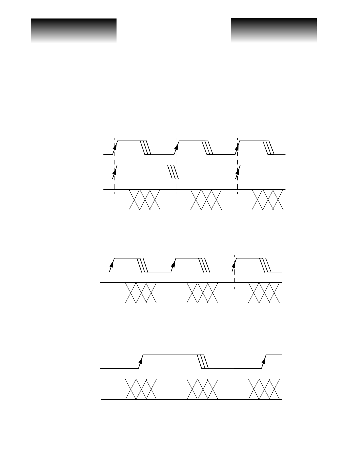
The following figures show the possible relationships between data and control inputs and the selected
input timing source. Figu re 2 shows how REFCLK is use d as an i nput t imi ng ref er en ce. Th is mod e of oper at ion
is also used in the VSC72 11 and VSC7214. Figure 3 and Figure 4 show how TBC is used as an input tim ing
reference. When TBC is used to define a data eye as shown in Figure 4, it functions as an additional data input
that simply toggles every cycle.
Note that the REFCLK and TBC inputs are not use d directly to clock the input data. Instead, an internal
PLL generates edges aligned with the appropriate clock. The arrows on the rising edges of these signals define
the reference edge for the internal phase detection logic. An internal clock is generated at 1/10 the serial
transmit data rate that is locked to the selected input timing source. This is an especially important issue when
DUAL is HIGH and input timing is referenced to REFCLK, since the falling edge is NOT used. The internal
clock active edges are placed coincident with the REFCLK rising edges and halfway between the REFCLK
rising edges in this mod e.
Reserved
G52268-0, Rev 3.3 Page 3
04/10/01
© VITESSE SEMICONDUCTOR CORPORATION • 741 Calle Plano • Camarillo, CA 93012
Tel: (800)-VITESSE • FAX: (805) 987-5896 • Email: prodinfo@vitesse.com
Internet: www.vitesse.com
VITESSE
SEMICONDUCTOR CORPORATION
SEMICONDUCTOR CORPORATION
ESE
Preliminary Data Sheet
Gigabit Interconnect Chip
A similar situation exists when TBC is used to define a data eye; only the rising edges of TBC are used to
define the external data timing. The internal clock active edges are placed at 90× and 270× points b etween
consecutive TBC rising edges (which are assumed to be 360× apart).
Figure 2: Transmit Timing, TMODE(2:0) = 000
VSC7212
REFCLK
(DUAL = 0)
REFCLK
(DUAL = 1)
T(7:0)
C/D
Vali d
Valid Valid
WSEN
Figure 3: Transmit Timing, TMODE(2:0) = 10X
TBC
T(7:0)
C/D
Valid
Vali d Valid
WSEN
Figure 4: Transmit Timing, TMODE(2:0) = 11X (“ASIC-Friendly” Timing)
o
0
o
90
180
o
270
o
TBC
T(7:0)
C/D
Vali d
Vali d Valid
WSEN
360
o
Page 4 G52268-0, Rev 3.3
© VITESSE SEMICONDUCTOR CORPORATION • 741 Calle Plano • Camarillo, CA 93012
Tel: (800)-VITESSE • FAX: (805) 987-5896 • Email: prodinfo@vitesse.com
Internet: www.vitesse.com
04/10/01

Preliminary Data Sheet
VITESSE
VITESSE
SEMICONDUCTOR CORPORATION
SEMICONDUCTOR CORPORATION
VSC7212
8B/10B Encoder
The VSC7212 contains an 8B/10B encoder which translates the 8-bit input data on T(7:0) into a 10-bit
encoded data character. A C/D input is also provided which, along with KCHAR, allow the transmission of
special Fibre Channel Kxx.x characters (see Table 2). Note that KCHAR is a static input, and does NOT ha ve
the same input timing as T(7:0), C/D and WS EN. Normally C/D is LOW in order to transmit data. If C/D is
HIGH and KCHAR is LOW, then a Fibre Channel defined IDLE Character (K28.5 = ‘0011111010’ or
‘1100000101’ depending on disparity) is transmitted and T(7:0) is ignored. If C/D is HIGH and KCHAR is
HIGH, a Kxx.x character is transm itted as determined by the data on T(7:0) (see Table 3). Data patterns other
than those defined in Table 3 produce undefined 10B encodings.
Table 2: Transmit Data Controls
WSEN C/D KCHAR Encoded 10- bit Output
0 0 X Data Character
0 1 0 IDLE Character (K28.5)
0 1 1 Special Kxx.x Character
1 X X 16-Character Word Sync Sequence
Gigabit Interconnect Chip
Table 3: Special Characters (Selected when C/D and KCHAR are HIGH)
Code T(7:0) Comment Code T(7:0) Comment
K28.0 000 11100 User Defined K28.6 110 11100 User Defined
K28.1 001 11100
K28.2 010 11100
K28.3 011 11100
K28.4 100 11100
K28.5 101 11100 IDLE K30.7 111 11110 User Defined
Encoder Bypass Mode
When ENDEC is LOW the 8B/10B encoder is by passed and a 10-bit inpu t character T(7:0) is seria lized
onto PTX/RTX with bit T0 is transmitted first. The C/D input becomes T8, and WSEN becomes T9. The
KCHAR input becomes ENCDET which is not us ed in the transmitter, but when HIGH, enables “Comma”
detection in the receiver. Refer to the “Decoder Bypass Mode” section for a description of this mode of
operation in the receiver. The latency through the transmitter is reduced by one character time when ENDEC is
LOW. This mode of opera tio n is sim ilar to a 10 -bit i n terfac e c omm only f ound in se ri alize r/de ser iali zers fo r the
Fibre Channel (e.g., VSC7125) and Gigabit Ethernet markets (e.g., VSC7135).
User Defined K28.7 111 11100 Test Only
User Defined K23.7 111 10111 User Defined
User Defined K27.7 111 11011 User Defined
User Defined K29.7 111 11101 User Defined
G52268-0, Rev 3.3 Page 5
04/10/01
© VITESSE SEMICONDUCTOR CORPORATION • 741 Calle Plano • Camarillo, CA 93012
Tel: (800)-VITESSE • FAX: (805) 987-5896 • Email: prodinfo@vitesse.com
Internet: www.vitesse.com

VITESSE
SEMICONDUCTOR CORPORATION
SEMICONDUCTOR CORPORATION
ESE
Preliminary Data Sheet
Gigabit Interconnect Chip
Word Sync Generation
The VSC7212 can perform chip-to-chip alignment (also referred to as “word alignment” or “word sync”),
meaning that the receive data output streams from multiple chips are aligned such that the same n-byte word
presented to the n transmit channels for serialization will be transferred on the receive channel parallel outputs.
The Word Sync Sequence provides a unique synchronization point in the serial data stream that is used to align
the receive channels. This sequence consists of 16 consecutive K28.5 IDLE characters with disparity reversals
on the second and fourth characters. The Word Sync Sequence is sent either as “I+ I+ I- I- I+ I- I+ I- I+ I- I+ II+ I- I+ I-” or as “I- I- I+ I+ I- I+ I- I+ I- I+ I- I+ I- I+ I- I+”, depending on the transmitter’s running disparity at
the time the first IDLE character is serialized.
Transmission of the Word Sync Sequence is initiated when the WSEN input is asserted HIGH for one
character time (see Figure 5). When WSEN is HIGH, the C/D and T(7:0) inputs are ignored. The WSEN, C/D
and T(7:0) inputs are also ignored for the subsequent 15 character times. In Figure 5, the Word Sync Sequence
is initiated in cycle W1 and transmitted through cycle W16. Normal data transmission (or the transmission of
another Word Sync Sequence) resumes in cycle D3. This figure is drawn assuming that input timing is
referenced to REFCLK (e.g. TMODE(2:0)=000) with the DUAL input LOW. As long as WSEN remains
asserted, another Word Sync Sequence will be generated.
Figure 5: Word Sync Sequence Generation
VSC7212
D2D1 W2W1 W4W3 W6W5 W8W7 W10W9 W12W11 W14W13 W16W15 D4D3
REFCLK
WSEN
C/D
T(7:0)
TX+/-
Serializer
The 10-bit output from the encoder (or from the skew buffer if ENDEC is LOW) is fed into a multiplexer
which serializes the parallel data using the synthesized transmit clock. The least significant bit of the 10B data is
transmitted first. The VSC7212 has both primary and re dund ant ser ial out pu t ports, PTX and RTX, respectively,
which consist of differential PECL output buffers operating at either 10 or 20 times the REFCLK rate. The
primary and redundant transmitter outputs are separately controllable. The primary PECL outputs PTX are
enabled when the PTXEN input is HIGH, and the redundant PECL outputs RTX are enabled when the RTXEN
input is HIGH. When a PECL output is disabled, the associated output buffers do no t consume power and the
attached pins are un-driven.
0x020x01 XXXX XXXX XXXX XXXX XXXX XXXX XXXX XXXX 0x040x03
D2.0+D1.0+ K28.5+K28.5+ K28.5-K28.5- K28.5-K28.5+ K28.5-K28.5+ K28.5-K28.5+ K28.5-K28.5+ K28.5-K28.5+ K28.5-K28.5+ D4.0-D3.0+
Page 6 G52268-0, Rev 3.3
© VITESSE SEMICONDUCTOR CORPORATION • 741 Calle Plano • Camarillo, CA 93012
Tel: (800)-VITESSE • FAX: (805) 987-5896 • Email: prodinfo@vitesse.com
Internet: www.vitesse.com
04/10/01

Preliminary Data Sheet
VITESSE
VITESSE
SEMICONDUCTOR CORPORATION
SEMICONDUCTOR CORPORATION
VSC7212
Gigabit Interconnect Chip
Receiver Functional Description
Serial Data Source
The receiver has both primary and redundant serial input ports, PRX and RRX, respectively, which consist
of differential PECL input buffers. It also has a control input, RXP/R, used to select either the primary or
redundant serial input as the data source. When RXP/R is HIGH, the serial data source is PRX. When
LBEN(1:0)=10, the transmitter is looped back and becomes the ser ial data source regardless of the state of
RXP/R (see Table 4).
T able 4: Serial Data Source Selection
LBEN(1:0) RXP/R Serial Data Source
≠ 1 0 0 RRX
≠ 1 0 1 PRX
= 1 0 X LBTX (Loopback from PTX/RTX)
Signal Detection
The primary and redundant PECL input buffers have an associated signal detect output, PSD ET and
RSDET. Both outputs are available for continuous monitoring of the selected and non-selected input. Each
signal detect output is asserted HIGH when transit ions are det ected on the associated PECL input and the signal
amplitude exceeds 200mV. A LOW indicates that either no transitions are detected o r the signal am plitude is
below 100mV. The signal detect outputs are consider ed undefine d when th e signal ampli tude is in the 100mV to
200mV range. The signal detect circuitry behaves like a re-triggerable one shot that is triggered by signal
transitions, and whose time-out interval ranges from 40 to 80 bit times. The transition density is not checked to
make sure that it corresponds to a valid Fibre Channel data stream. The PSDET an d RSDET output timing is
identical to the low-speed receiver outputs, as selected by RMODE(1:0) in Table 5.
Receiver Equalization
Incoming data on the PRX/RRX input typically contains a substantial amount of Inter Symbol Interference
(ISI) or deterministic jitter which reduces the ability of the receiver to recover data without errors. An equalizer
has been added to each of the recei ver ’s input buffers in order to compensate for this deterministic jitter. This
circuit has been designed to effectively reduce the IS I commonly found in co pper cabl es or backp lane traces d ue
to low frequencies traveling faster than high frequencies as a result of the skin effect. The equalizer boosts high
frequency edge response in order to reduce the adverse effects of ISI.
G52268-0, Rev 3.3 Page 7
04/10/01
© VITESSE SEMICONDUCTOR CORPORATION • 741 Calle Plano • Camarillo, CA 93012
Tel: (800)-VITESSE • FAX: (805) 987-5896 • Email: prodinfo@vitesse.com
Internet: www.vitesse.com

VITESSE
SEMICONDUCTOR CORPORATION
SEMICONDUCTOR CORPORATION
ESE
Preliminary Data Sheet
Gigabit Interconnect Chip
Clock and Data Recovery
The receiver has a Clock Recovery Unit (CRU) which accepts the selected serial input source, extracts the
high-speed clock and retimes the data. The CRU is monol ithic. The CRU automatically locks on data and if the
data is not present, will automatically lock to the REFCLK. This maintains a very well-behaved recovered
clock, RCLK/RCLKN which does not contain any slivers and will operate at a frequency of the REFCLK
reference +/- 200 ppm. The use of an external Lock-to-Reference pin is not needed.
The Clock Recovery Unit must perform bit synchronization which occu rs when the CRU locks onto and
properly samples the incoming serial data as described in the previous paragraph. When the CRU is not locked
onto the serial data, the 10-bit data out of the decoder is invalid which results in numerous 8B/10B decoding
errors or disparity errors. When the link is disturbed (e.g., the cable is disconnected or the serial data source is
switched), the CRU will require a certain amount of time to lock onto data, which is specified in the AC Timing
Specification for “Data Acquisition Lock Time.”
Deserializer and Character Alignment
The retimed serial data stream is converted into 10-bit characters by the deserializer. A special 7-bit
“Comma” pattern (‘0011111xxx’ or ‘1100000xxx’) is recognized by the receiver and allows it to identify the
10-bit character boundary. Note that this pattern is found in three special characters, K28.1, K28.5 and K28.7.
However, K28.5 is chosen as the unique IDLE character. Only K28.1 and K28.5 should be used in norma l
operation. The K28.7 character should be reserved for test and characterization use.
Character alignment occurs when the deserializer synchronizes the 10-bit character framing boundary to a
“Comma” pattern in the incoming serial data stream. If the receiver identifies a “Comma” pattern in the
incoming data stream which is misaligned to the current framing boundary the receiver will re-synchronize the
recovered data in order to align the data to the new “Comma” pattern. Re-synchronization ensures that the
“Comma” character is output on the internal 10-bit bus so that bits 0 through 9 equal ‘0 011111x xx’ or
‘1100000xxx’. If the “Comma” pa ttern is align ed with the current framing bo undary, then re-synchronization
will not change the current alignment. Re-synchronization is always enabled and cannot be turned off when
ENDEC is HIGH. After character re-synchronization the VSC7212 ensures that within a link, the 8-bit data sent
to the transmitting VSC7212 will be recovered by the receiving VSC7 212 in the same bit locations as the
transmitter (i.e. T(7:0) = R(7:0)). When ENDEC is LOW , “Comma” detection and al ignmen t are enabled on ly if
KCHAR is HIGH.
VSC7212
10B/8B Decoder
The 10-bit character from the deseriali zer is dec oded in t he 10B/8B decod er, which outputs th e 8B data byt e
and three bits of status i nformat ion. If the 1 0-bit c haracter does not match a ny vali d valu e, an Out- of-Band Err or
is generated which is output on the receiver status bus. Similarly, if the running disparity of the character does
not match the expe cted va lue, a Disp arity Err or is gen erated. T he decode r also repo rts whe n a K-char acter is
received, and distinguishes the K28.5 (IDLE) cha racter from other K-char acters. This status information is
combined with LOS State Machine status and FIFO error status, to produce the prioritized per-character link
status output information (se e Table 7).
Page 8 G52268-0, Rev 3.3
© VITESSE SEMICONDUCTOR CORPORATION • 741 Calle Plano • Camarillo, CA 93012
Tel: (800)-VITESSE • FAX: (805) 987-5896 • Email: prodinfo@vitesse.com
Internet: www.vitesse.com
04/10/01

Preliminary Data Sheet
VITESSE
VITESSE
SEMICONDUCTOR CORPORATION
SEMICONDUCTOR CORPORATION
VSC7212
Elastic Buffer and Channel De-Skewing
An elastic buffer is included in the receiver. Decoded data and status information is written into these
buffers with the recovered clock, and is read with the selected word clock (either the recovered clock or
REFCLK). In addition to allowing decoded data to easily cross from a receiver’s recovered clock domain to its
output clock domain, the elastic buffer facilitates chip-to-chip alignment (the reconstruction of a multi-byte
word as presented to the transmitting devices), and facilitates rate matching v ia IDLE character insertion/
deletion when the receiver’s recovered clock is not frequency-locked to its selected word clock.
There are three conditions under which a receiver ’s elasticity buffer is recentered. The RESETN input,
when asserted LOW, recenters the read/write pointers in the elasticity buffer . Whenever a “Comma” charact er is
received which changes the receive character’s frami ng boun dar y, the elasticity buffer is recentered. Lastly, it is
also recentered whenever the receiver detect s the synchroni zation po int in the Word Sync Sequence. All three of
these events are associated with chip initialization or link initialization and would not occur during normal data
transfer. Note that recentering can result in the loss or duplication of decoded character data and status
information.
When a condition ch anges transmit timing (e.g., pha se shifts in TBC ) or shifts pha se/alignment into the
receiver, the user should resend a Word Sync Event or assert RESETN in order to recenter the elasticity buffer.
Otherwise, data corruption could occur. It is unsafe to assume that after a change in transmit timing that
“Comma” characters will be misaligned and will cause recentering
The VSC7212 presents recovered data on R(7:0) and status on IDLE, KCH and ERR. These outputs are
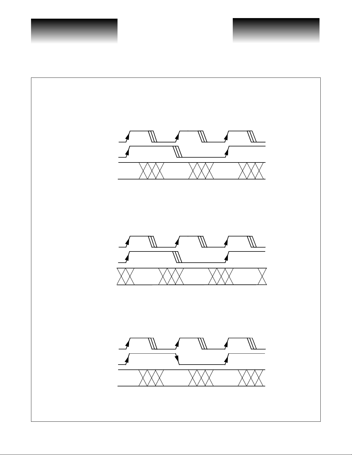
timed either to the receiver’s recovered clock (RCLK/RCLKN) or to REFCLK. The output timing reference is
selected by RMODE(1:0) (see Table 5). TBERR, PSDET and RSDET are also synchronized to the selected
word clock. There are two choices for REFCLK-based timing, which differ in the positioning of the data valid
window associated with the output signals timed to REFCLK. When RMODE(1:0)=00 REFC LK is
approximately centered in the output data valid window as in the VSC7211 or VSC7214. When
RMODE(1:0)=01 REFCLK slightly leads the data valid window so that output data appears to have a more
typical “Clock-to-Q” timing relationship t o REFCLK.
Gigabit Interconnect Chip
T able 5: Receive Interface Output Timing Mode
RMODE(1:0) Output Timing Reference
0 0 REFCLK (Centered)
0 1 REFCLK (Leading)
1 X RCLK/RCLKN
The term “word cloc k” will be used for whichever clock, REFCLK or RCLK/RCLKN, is selected as the
output timing reference. If RM ODE(1) i s HIGH, t he receiver ’s RCLK/RCLKN outputs are complementary
outputs at 1/10th or 1/20th the baud rate of the incoming data depending upon DUAL. If RMODE(1) is LOW,
then the RCLK/RCLKN outputs are held HIGH/LOW and the data bus and status outputs are timed to
REFCLK. If DUAL is HIGH, all data at the receiver’s output p ort is syn chrono usly clocked out on both po siti ve
and negative edges of the selected word clock at 1/20th the baud rate. If DUAL is LOW, the data is clocked out
G52268-0, Rev 3.3 Page 9
04/10/01
© VITESSE SEMICONDUCTOR CORPORATION • 741 Calle Plano • Camarillo, CA 93012
Tel: (800)-VITESSE • FAX: (805) 987-5896 • Email: prodinfo@vitesse.com
Internet: www.vitesse.com
VITESSE
SEMICONDUCTOR CORPORATION
SEMICONDUCTOR CORPORATION
ESE
Preliminary Data Sheet
Gigabit Interconnect Chip
of the VSC7212 only on the rising edge of the selected word clock at 1/10th the baud rate. Timing waveforms
for the output data and status are shown in Figure 6, Figure 7 and Figure 8.
Figure 6: Receive Timing, RMODE(1:0) = 00
REFCLK
(DUAL = 0)
REFCLK
(DUAL = 1)
R(7:0)
IDLE
KCH
ERR
Valid
Figure 7: Receive Timing, RMODE(1:0) = 01
Vali d Vali d
VSC7212
REFCLK
(DUAL = 0)
REFCLK
(DUAL = 1)
R(7:0)
IDLE
KCH
ERR
RCLK
(DUAL = 0)
RCLK
(DUAL = 1)
R(7:0)
IDLE
KCH
ERR
V alid
Figure 8: Receive Timing, RMODE(1:0) = 1X
Vali d
V alid V alid
V alid V alid
Page 10 G52268-0, Rev 3.3
© VITESSE SEMICONDUCTOR CORPORATION • 741 Calle Plano • Camarillo, CA 93012
Tel: (800)-VITESSE • FAX: (805) 987-5896 • Email: prodinfo@vitesse.com
Internet: www.vitesse.com
04/10/01

Preliminary Data Sheet
VITESSE
VITESSE
SEMICONDUCTOR CORPORATION
SEMICONDUCTOR CORPORATION
VSC7212
If RMODE1 is LOW and if the transm itting device’s REFCLK is not precisely frequency-locked to a
receiver’s REFCLK, then the channel’s elastic buffer will tend to gradually fill or empty as the recovered clock
(which is by definition frequency-locked to the transmitter’s REFCLK) steadily drifts in phase relative to the
word clock. In order to accommodate freq uency dif feren ces between a transmi tter’s REFCLK and the rec eiver’s
REFCLK, the VSC7212 can automatically perform “rate matching” by either deleting or duplicating IDLE
characters. FLOCK must be LOW and WSI must be connected to WSO to enable rate matching. It is the user’s
responsibility to ensure that the frequency at which IDLEs are transmitted accommoda tes the frequency
differences, if any, in their system architecture. Not meeting the IDLE density requirements described below
may result in Underrun/Overrun Errors.
The elastic buffer is designed to allow a maximum phase drift of +2 or -2 serial clock bit times between resynchronizations, which sets a limit on the maximum data “packet” length allowed between IDLEs. This
maximum packet length depends on the frequency difference between the transmitting an d receiving devices
REFCLKs. Let represent phase drift in bit times, and let represent one full 10-bit character of phase
drift. Limiting phase drift to two bit times means the following inequality must be sat isfie d:
(1)
Let L be the number of 10-bit characters transmitted, and let
phase drift in bit times is given by:
∆φ 2π
∆φ 0.2 2π×()≤
Df be the frequen cy offset in ppm. The total
Gigabit Interconnect Chip
(2)
A simple expression for maximum packet len gt h as a fun c tion of frequency offs et is derived by substituting
(2) in (1) and solving for L:
(3)
As an example, if the frequen cy of fset is 20 0ppm, the n the maxi mum packet length sho uld not be more th an
1K bytes. To increase the maximum packet length L, decrease the frequency offset
K28.5 is transmitted between “packets” of data, it might be dropped during compensation for phase drift. If the
user must have at least one K28.5 between these two packets, then two K28.5s must be transmitted.
Using Multiple VSC7212s in Parallel
Multiple VSC7212s and VSC7216s can be used in parallel to form wider bus widths. In order for chip-tochip word alignment to function corr ectly across multiple devices, e ach transm it channel’s input data must be
transmitted synchronously to a common REFCLK or TBC, and each re cei ver’s output data must also be aligned
to a common REFCLK. Th is requir es that a ll transm itting devices use either the sam e or ident ical REFCL Ks,
and that TMODE(2:0)=000 (inputs timed to REFCLK) or TMODE(2:0)=1X0 (inputs timed to TBC). If inputs
are timed to TBC, then all transmitting devices must use either the same or identical TBCs. Since all receive
channels must use a common word clock, the receiving devices must also use the same or identical REFCLKs
and it must be selected as the word clock for all receive channels (RMODE(1:0)=0X).
∆φ ∆f 10
L 0.2 10
6
⁄()2π× L=
6
×()∆f⁄≤
Df. Note that if on ly one
G52268-0, Rev 3.3 Page 11
04/10/01
© VITESSE SEMICONDUCTOR CORPORATION • 741 Calle Plano • Camarillo, CA 93012
Tel: (800)-VITESSE • FAX: (805) 987-5896 • Email: prodinfo@vitesse.com
Internet: www.vitesse.com
 Loading...