

VITESSE VSC7186TW Datasheet
VITESSE
SEMICONDUCTOR CORPORATION
Advance Product Information
VSC7186
Quad Transceiver
for Gigabit Ethernet
Features
• Four Complete Transceiver Functions in One IC
• Full Gigabit Ethernet (IEEE 802.3z) Complian ce
• Pin-Compatible With Agilent HDMP-1686A
• 5-Volt Tolerant TTL Inputs
• Uses Reference Clock to Latch Tx Data
th
• 1/10
or 1/20th Baud Rate Recovered Clocks
• Common Local Loopback Control
• Single Comma Detect Enable
• Cable Equalization in Receivers
• Automatic Lock-to-Reference
• JTAG Access Port
• 2kV ESD Protection on All Pins
• 3.3V Power Supply, 2.67 W Max Dissipation
• 208 pin, 23 mm BGA Packaging
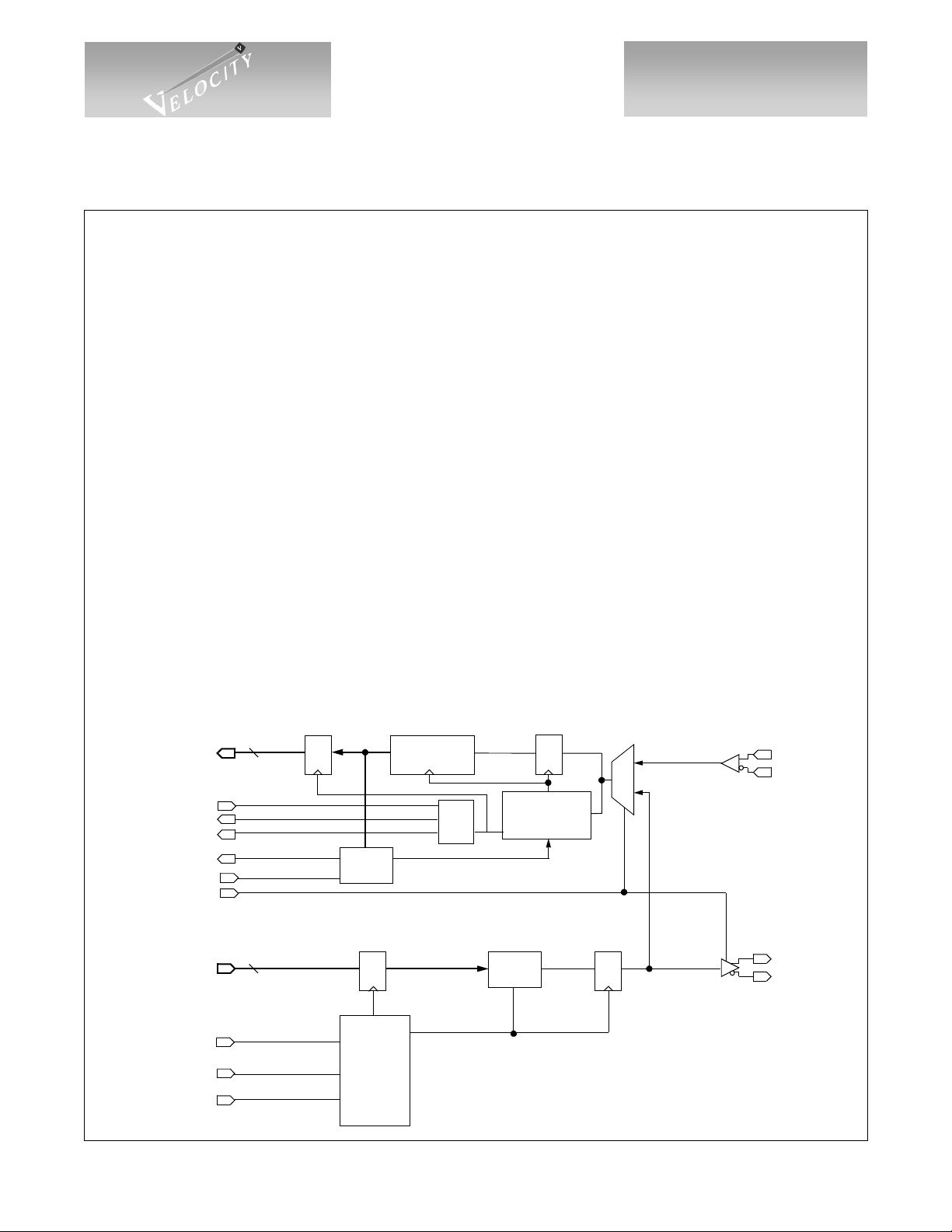
General Description
The VSC7186 is a Quad Gigabit Ethe rnet Transceiver IC. Each of the four trans mitters has a 10 -bit wide
bus, running at 125 MHz, which accepts 8b/10b encoded transmit characters and serializes the data onto high
speed differential outputs at rates be tween 1.05 an d 1.36 Gb/s. Th e transmit data must be sync hronous to the
reference clock. Each receiver samples serial receive data, recovers the clock and data, deserializes it into 10-bit
receive characters, outputs a recovered clock and detects “Comma” characters. The VSC7186 contains on-chip
PLL circuitry for synthesis of the baud-rate transmit clock and extraction of the clocks from the received serial
streams.
VSC7186 Block Diagram (1 of 4 Channels)
RXi(0:9)
RCM
RCi1
RCi0
SYNi
SYNC
LOOP
TXi(0:9)
RFC1
CAP0
CAP1
10
10
Q D
Comma
Detect
Clock
Multiply
Serial to
QD
Parallel
SEL
÷10/
÷20
Unit
x10
Recovery
÷10
Parallel
to Serial
Q D
Clock
Unit
0
1
D QD Q
SI+
SI-
SO+
SO-
G52306-0, Rev. 2.0
3/27/00 741 Calle Plano, Camarillo, CA 93012 • 805/388-3700 • FAX: 805/987-5896
VITESSE SEMICONDUCTOR CORPORATION Page 1
VITESSE
SEMICONDUCTOR CORPORATION
Quad Transceiver
for Gigabit Ethernet
Advance Product Information
VSC7186
Functional Description
Notation
In this document, each of the four channels are identified as Channel 0, 1, 2 or 3. When discussing a signal
on any specific channel, the signal will have the Channel number embedded in the name, i.e. “T3(0:9)”. When
referring to the common beha vior of a sign al whic h is used on e ach of th e four c hanne ls, th e notat ion “i” is used.
Differential signals, i.e. SOi+ and SOi-, may be referred to as a single signal, i.e. SOi, by dropping reference to
the “+” and “-”.
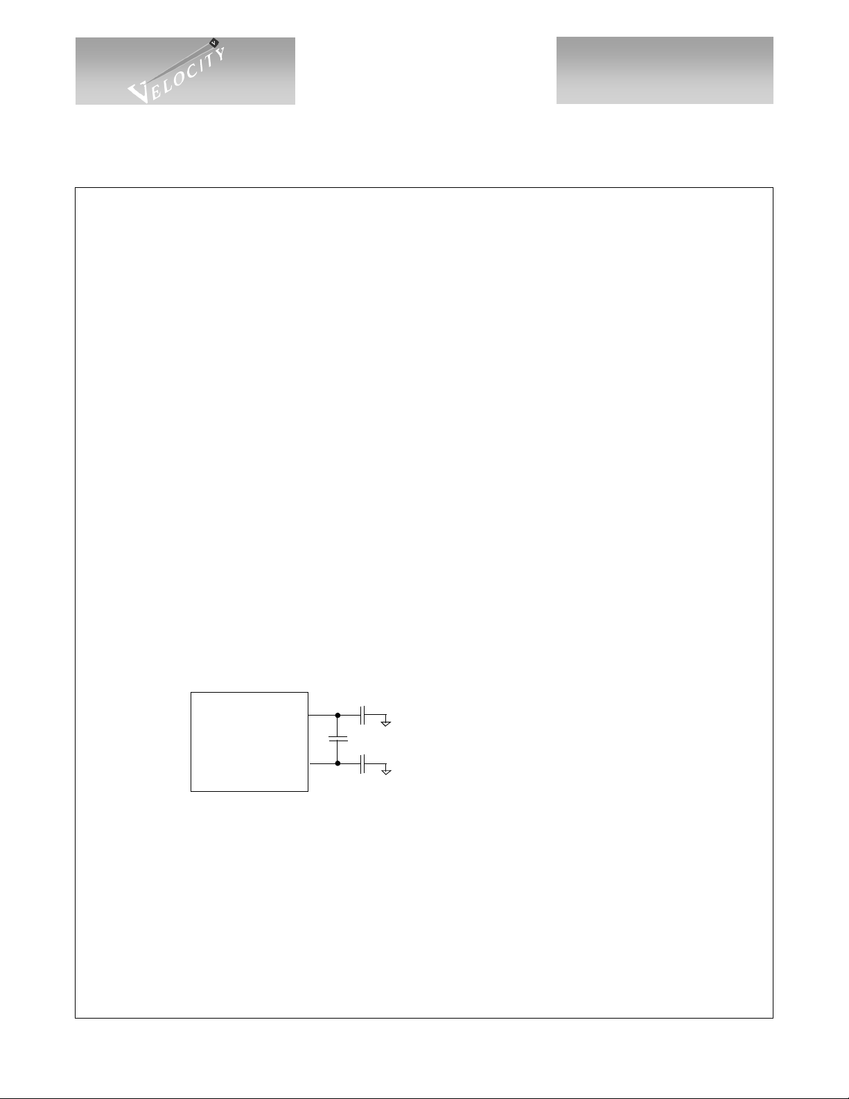
Clock Synthesizer
The VSC7186 Clock Multiplier Unit (CMU) multiplies the reference frequen cy provided on the RFC1
input by 10 to achieve a bau d rate cloc k betwe en 1.05 and 1.3 6 GHz. The RFC 1 input is TTL. The on -chi p PLL
uses a single external 0.1uF capacitor, connected between CAP0 and CAP1, to control the Loop Filter. This
capacitor should be a multilayer ceramic dielectric, or better, with at least a 5V working voltage rating and a
good temperature coefficient, i.e., NPO is preferred but X7R may be accep table. These capacitors are us ed to
minimize the impact of common mode noise on the Clock Multiplier Unit, especially power supply noise.
Higher value capacitors provide better robustness in systems. NPO is preferred because if an X7R capacitor is
used, the power supply noise sensitivity will vary with temperature.
For best noise immunity, the designer may use a three capacitor circuit with one differential capacitor
between CAP0 and CAP 1, C1, a capa citor from CAP0 to ground, C2, an d a capacitor f rom CAP1 to groun d,
C3. Larger values are better but 0.1uF is ad equate. However, if the designer can not use a thre e capaci tor circu it,
a single differential capacitor, C1, is adequate. These components should be isolated from noisy traces.
Figure 1: Loop Filter Capacitors (Best Circuit)
CAP0
VSC7186
CAP1
Serializer
The VSC7186 accepts TTL input d ata as four parallel 10 bit characters on the Ti(0:9) buses which are
latched into the input registers on the rising edge of RFC1. The 10-bit parallel transmission character will be
serialized and transmit ted on the SOi+ /- PECL di fferential outp uts a t the ba ud rate with bi t Ti0 (bit a) transmit ted first. User data should be encoded using 8b/10b or an equivalent code. The mapping to 10b encoded bit
nomenclature and transmission order is illustrated below, along with the recognized comma pattern.
Page 2 VITESSE SEMICONDUCTOR CORPORATION
741 Calle Plano, Camarillo, CA 93012 • 805/388 -37 00 • FAX: 805/987-5896 3/27/00
C1
C2
C3
C1=C2=C3= >0.1uF
MultiLayer Ceramic
Surface Mount
NPO (Prefered) or X7R
5V Working Voltage Rating
G52306-0, Rev. 2.0
VITESSE
SEMICONDUCTOR CORPORATION
Advance Product Information
VSC7186
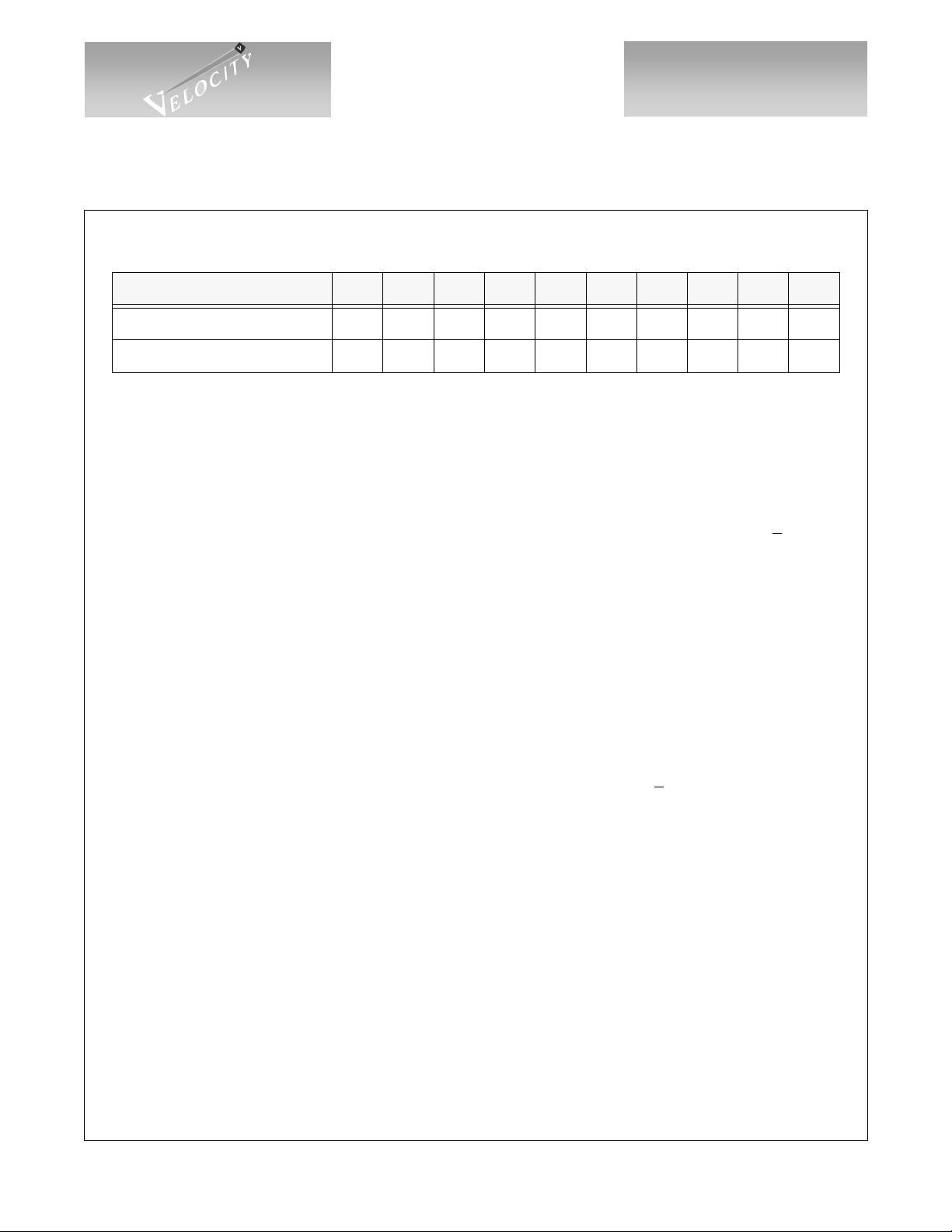
Table 1: Transmission Order and Mapping of a 10b Character
Data Bit
10B Bit Position j h g f i e d c b a
Comma Character xxx1111100
Clock Recovery
The VSC7186 accepts differential high speed serial input from the selected source (either the PECL SIi+/pins or the internal SOi+/- data), extracts the clock and retimes the data. Equalizers are included in the receiver
to open the data eye and compensate for Intersymbol Interference (ISI) w hich may be present in t he incoming
data. The serial bit stream should be encoded so as to provide DC balance and limited run length by an 8b/10b
encoding scheme. The digital Clock Recovery Unit (CRU) is completely monolithic and requires no external
components. For proper operation, the baud rate of the data stream to be recovered should be within +
of ten times the REF frequency. For example, Gigabit Ethernet systems use 125 MHz oscillators with a +/100ppm accuracy resulting in +/-200 ppm between VSC7186 pairs.
Deserializer
The recovered serial bit stream is converted into a 10-bit parallel output character. The VSC7186 provides
complementary TTL recovered clocks, RCi0 and RCi1, at one-twentieth of the serial baud rate if RCM=LOW,
or a single clock at one-tenth the serial baud rate, on RCi1 only, if RCM=HIGH. The clocks are generated by
dividing down the high-speed recovered clock which is phase locked to the serial data. The serial data is
retimed, deserialized and output on Ri(0:9).
If serial input data is not present, or does n ot meet the req uired baud rate , the VSC7186 will c ontinue to
produce a recovered c lock so that downstream l ogic may continue to func tion. The R Ci0/RCi1 o utp ut fre quency
under these circumstances will differ from its expected frequency by no more than +
T9 T8 T7 T6 T5 T4 T3 T2 T1 T0
1%.
Quad Transceiver
for Gigabit Ethernet
200 ppm
Word Alignment
The VSC7186 provides 7-bit comma character recognition and data word alignment. Wor d sync hr oni zati on
is enabled on all channels by asserting SYNC HIGH. When synchronization is enabled, the receiver examines
the recovered seria l data for th e presence of the “Comma” pattern. This pattern is “0011111XXX”, where the
leading zero corresponds to the first bit received. The comma sequence is not contained in any normal 8b/10b
coded data character or pair of adjacent characters. It occurs only within special characters, known as K28.1,
K28.5 and K28.7, which ar e defined f or sync hronizat ion purpo ses. Imp roper com ma alignm ent is defi ned as
any of the following conditions:
1) The comma is not aligned within the 10-bit transmission character such that Ri(0..6) = “0011111”.
2) The comma straddles the boundary between two 10-bit transmission characters.
3) The comma is properly aligned but occurs in the recei ved character presented duri ng the rising edge of
RCi0 rather than RCi1.
When an improperly aligned comma is encounte red, the recovered clock is st retch ed, never sliv ered, so that
the comma character and recovered clocks are aligned properly to Ri(0:9). This results in proper character and
word alignment. When the parallel data alignment changes in response to a improperly aligned comma pattern,
G52306-0, Rev. 2.0
3/27/00 741 Calle Plano, Camarillo, CA 93012 • 805/388-3700 • FAX: 805/987-5896
VITESSE SEMICONDUCTOR CORPORATION Page 3
VITESSE
SEMICONDUCTOR CORPORATION
Quad Transceiver
for Gigabit Ethernet
data which would have been presented on the parall el output port prior to the comma charact er, and possibly the
comma character itself, may be lost. Possible loss of the comma character is data dependent, acc ording to the
relative change in al ignment. Data subsequent to the comma character will alway s be out put co rrectly and properly aligned.
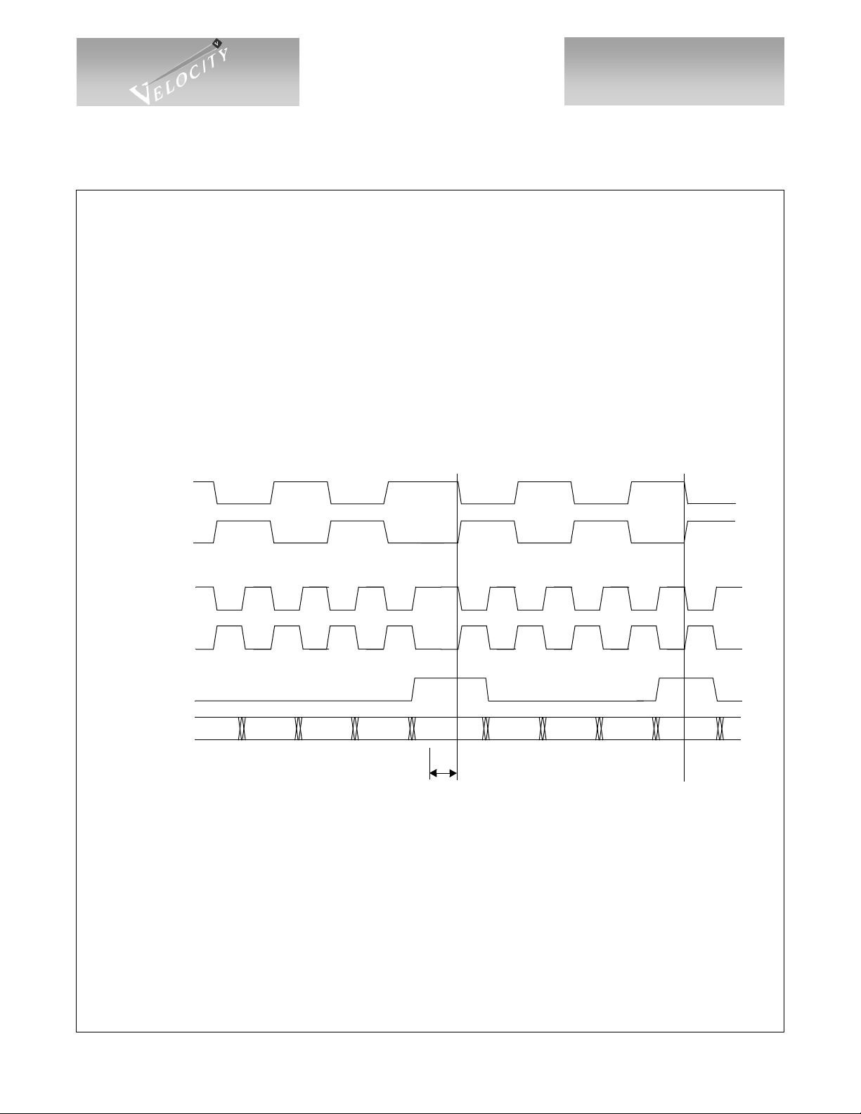
On encountering a comma character, SYNi is driven HIGH. The SYNi pulse is presented simu ltaneousl y
with the comma character and has a durat ion equ al to t he da ta. The SYNi signal i s t imed such that it can be captured by the adjoining protocol logic on the rising edge of RCi1. Functional waveforms for synchronization are
given in Figure 1. The first K28.5 shows the case where the comma is detected, but it is misaligned so a change
in the output data alignment is requ ired. Note t hat up to thr ee charac ters prior to the comma ch aracter ma y be
corrupted by the realignment process . The second K28.5 shows the case when a comma is detec ted and no
phase adjustment is necessary. It illustrates the positi on of the SYNi pulse in relati on t o the comma ch aract er on
Ri(0:9).
Figure 2: Misaligned and Aligned K28.5 Characters
RCi0
(RCM LOW)
i1
RC
Advance Product Information
VSC7186
i0
RC
(RCM HIGH)
i1
RC
i
SYN
RXi(0:9)
Loopback Operation
Loopback operation is controlled by the LOOP line. When this line is HIGH, the outgoing high-s peed
serial data on each of the four channels is internally looped back into that channel’s high-speed serial receiver
section. This provides for in-circuit tes ting capability independent of the tran smission medium.
JT AG Access Port
A JTAG access port is provided t o assist in board-l evel t esti ng. Thro ugh this port most pins can be acc essed
or controlled and all TTL outputs can be tri-stated. A full description of the JTAG functions on this device is
available in “VSC7186 JTAG Access Port Functionality”. Circuits designed exclusively for the HDMP-1686A
will automatically disable the JTAG port. The pinout table in this data sheet shows the proper connections for
either HDMP-1686A emulation or for JTAG functionality (in parentheses).
Corrupt Corrupt Corrupt K28.5 Data1 Data2 Data3 K28.5Data
Misaligned Comma: Stretched
Aligned Comma
Page 4 VITESSE SEMICONDUCTOR CORPORATION
741 Calle Plano, Camarillo, CA 93012 • 805/388 -37 00 • FAX: 805/987-5896 3/27/00
G52306-0, Rev. 2.0
VITESSE
SEMICONDUCTOR CORPORATION
Advance Product Information
VSC7186
AC Characteristics
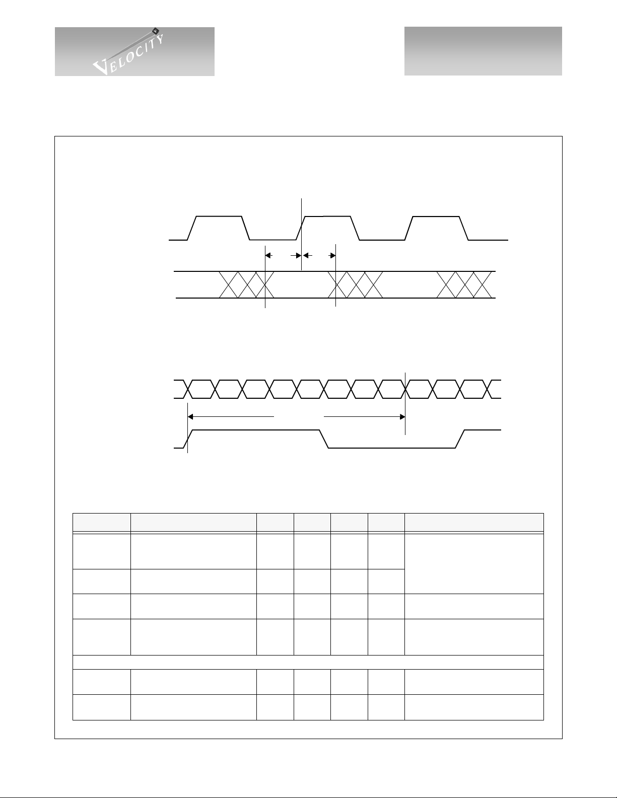
Figure 3: Transmit Timing Waveforms
RFC1
TXi(0:9)
10 Bit Data
+/-SOi
Data Valid
T
1
Data Valid
Quad Transceiver
for Gigabit Ethernet
T
2
Data Valid
S0 S1 S2
T
LAT
RFC1
Table 2: Transmitter AC C haracteristics
Parameter Description Min Typ Max Units Conditions
T
1
T
2
T
SDR,TSDF
T
LA T
RJ Random jitter (RMS) — 58ps.
DJ
Ti(0:9) Setu p time to th e risi ng
edge of RFC1
Ti(0:9) hold time after the
rising edge of RFC1
Ti+/Ti- rise and fall time ——300 ps.
Latency from rising edge of
RFC1 to Ti0 appearing on SO
bit 0i
Serial data output deterministic
jitter (pk-pk)
1.5 ——ns.
1.0 ——ns.
7bc +
0.66ns
Transmitter Output Jitter
— 35 80 ps.
—
7bc +
1.46ns
Note:
Measured between the valid data
level of Ti(0: 9) to the 1.4V po int of
RFC1
20% to 80%, 75 Ohm load to Vdd/
2, Tested on a sample basis
bc = bit clocks
ns = nanoseconds
Measured at SO+/-, 1 sigma
deviation of 50% cr ossing pt
IEEE 802.3Z Clause 38.6 8, Tested
on a sample basis
G52306-0, Rev. 2.0
3/27/00 741 Calle Plano, Camarillo, CA 93012 • 805/388-3700 • FAX: 805/987-5896
VITESSE SEMICONDUCTOR CORPORATION Page 5
 Loading...