

VITESSE VSC7185TW Datasheet
VITESSE
SEMICONDUCTOR CORPORATION
Preliminary Data Sheet
VSC7185
Quad Transceiver for
Gigabit Ethernet and Fibre Channel
G52324-0, Rev 3.1 Page 1
03/25/01
© VITESSE SEMICONDUCTOR CORPORATION • 741 Calle Plano • Camarillo, CA 93012
Tel: (800) VITESSE • FAX: (805) 987-5896 • Email: prodinfo@vitesse.com
Internet: www.vitesse.com
Features
General Description
The VSC7185 is a full-speed quad Gig abit Ethe rnet and Fibre Cha nnel T r ansceiv er IC. 8B/10 B encoded (or
equivalent scheme) transmit characters are serialized onto high-speed differential outputs (SOi+/-) at speeds up
to 1.36Gb/s. Each of the four transmitters has a 5-bit wide parallel input bus. Parallel data is latched in by an
internal clock running at up to 272MHz (2x the rate of the external common Transmit Byte Clock). Transmit
data must be presented synchronously with the common transmit byte clock. Each receiver samples the serial
receive data (SIi+/-), recovers the clock and data, deserializes it into 5-bit receive half-characters, outputs a
recovered 2x or 1x clock and detects “Comm a” characters . The VSC718 5 contains on-c hip PLL circuitry for
synthesis of the baud-rate transmit clock and extraction of the clocks from the received serial streams.
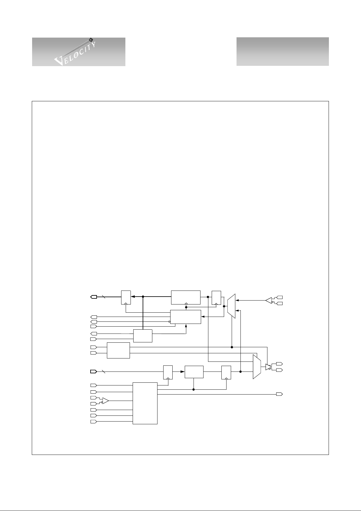
VSC7185 Block Diagram (1 of 4 Channels)
• Four Complete Tran sceiver Fun ctions in a Single
Integrated Circuit
• SSTL-2 Compatible Parallel Da ta and Clocks
• 1.05Gb/s to 1.36Gb/s Operation per Channel
• Common Transmit Byte Clock
• TTL or PECL Reference Clock Input
• Per-Channel 1/ 10
th
Baud Rate Recovered Clocks
and Comma Detect Outputs
• Common Comma Detect Enable Input
• Common Serial / Parallel Loopback Controls
• Cable Equalization in Receivers
• JTAG Access Port
• 3.3V Power Supply , 2. 5W Dissipation, Typical
• 208 pin, 23mm BGA Package
Loopback
Control
1
0
SIi+
SIi-
Q D
Serial to
Parallel
Comma
RXi(0:4)
Clock
Parallel
to Serial
SOi+
SOi-
5
5
Q D
QD
Detect
D Q
D Q
Multiply
Unit
x10/x20
1
0
RCi1
RCi0
SYNi
TXi(0:4)
RFCT
RSYN
PLUP
SYNC
CAP0
CAP1
÷
10
SLPN
TC
RFC+
RFC-
RFCM
RFCO
Clock
Recovery
Unit
÷
5
VITESSE
SEMICONDUCTOR CORPORATION
Preliminary Data Sheet
VSC7185
Quad Transceiver for
Gigabit Ethernet and Fibre Channel
Page 2 G52324-0, Rev 3.1
03/25/01
© VITESSE SEMICONDUCTOR CORPORATION • 741 Ca ll e Pl an o • Camarillo, CA 93012
Tel: (800) VITESSE • FAX: (805) 987-5896 • Email: prodinfo@vitesse.com
Internet: www.vitesse.com
Functional Description
Notation
In this document, each of the four channels are identified as Channel 0, 1, 2 or 3. When discussing a signal
on any specific channel, the signal will have the channel number embedded in the name, for example,
“TX3(0:4).” When referring to the common behavior of a signal which is used on each of the four channels, the
notation “i” is used. Differential signals, i.e. SOi+ and SOi-, may be referred to as a single signal, i.e. SOi, by
dropping reference to the “+” and “-”. R FC refers to the active reference clock input(s), RFCT or RFC+/RFC-.
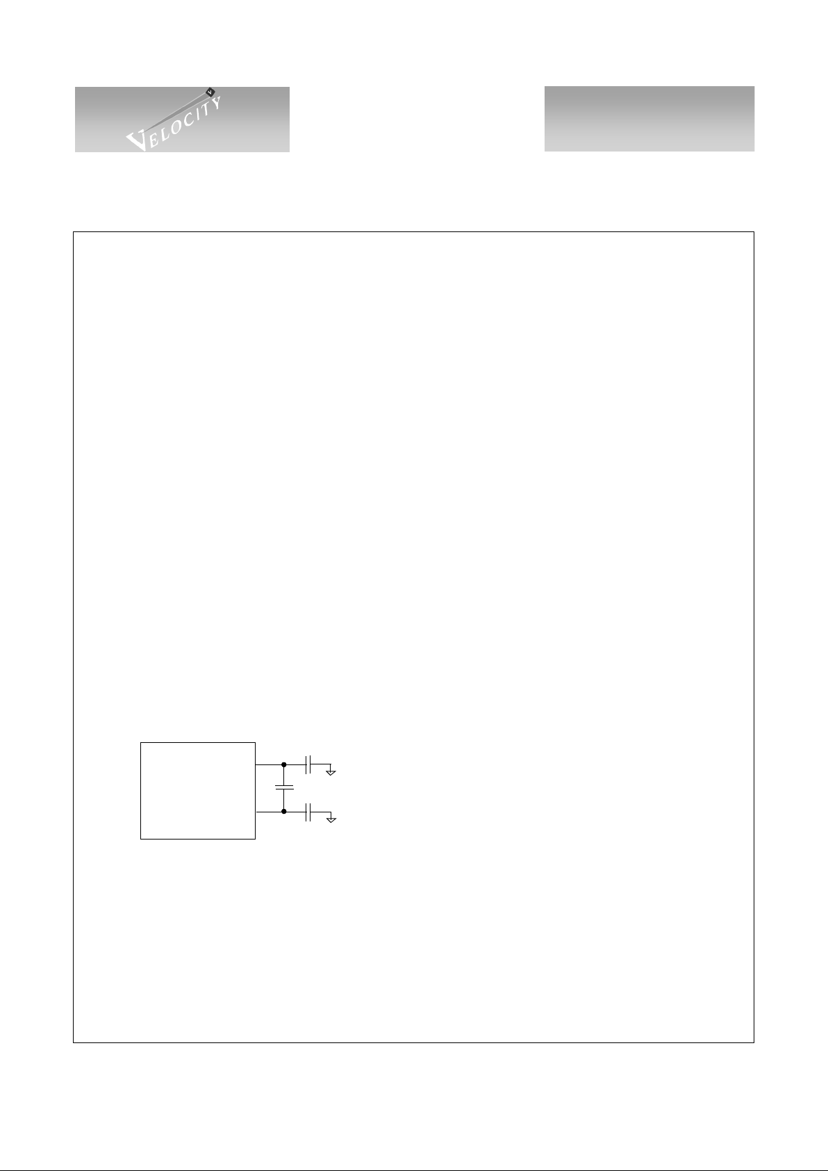
Clock Synthesizer
To achieve a baud rate clock between 1.05GHz and 1.36GHz, the VSC7185 Clock Multiplier Unit (CMU)
multiplies the reference frequency provided on the RFC input by 10 when RFCM=1, or by 20 when RFCM=0.
The RFCT input is TTL, and the REF+/- inputs are PECL. The on-chip PLL uses a single external 0.1
µF capac-
itor, connected between CAP0 and CAP1, to control the Loop Filter. This capacitor should be a multilayer
ceramic dielectric, or better, with at least a 5V working voltage rating and a good temperature coefficient. NPO
is preferred but X7R may be acceptabl e. These cap acitors are us ed to minimize the impact of common-mo de
noise on the Clock Multiplier Unit, especially p ower supply noise. Higher value cap acitors provide better
robustness in systems. NPO is preferred because if an X7R capacitor is used, the power supply noise sensitivity
will vary with temperature.
For best noise immunity, the designer may use a three capacitor circuit with one differential capacitor
between CAP0 and CAP1, C1, a capaci t or fr om C AP0 to ground, C2, and a capacitor from C AP1 t o ground, C3
(see Figure 1). Larger values are better but 0.1
µF is adequate. However, if the designer cannot use a three
capacitor circuit, a single differential capacitor, C1, is adequate. These components should be isolated from
noisy traces.
Figure 1: Loop Filter Capacitors (Best Circuit)
Serializer
The VSC7185 accepts 5-bit parallel SSTL-2 input data on the four TXi(0:4) buses along with an SSTL-2
byte clock (TC) and serializes them into four high-speed serial streams. At the source, TXi(0:4) and TC switch
synchronously with respect to an internal 5 bit-time clock. TC and RFC must be derived from the same frequency source so that TC and RFC have a fixed but arbitrary phase relationship when system clocks are stable.
The 5-bit parallel transmission half-characters will be serialized and transmitted on the SOi+/- PECL differential outputs at the baud rate, with bit TXi0 (10B bit “a” or “i”) transmitted first. User data should be encoded
using 8B/10B or an equivalent code.
CAP0
CAP1
C1
C2
C3
VSC7185
C1=C2=C3= >0.1uF
MultiLayer Ceramic
Surface Mount
NPO (Preferred) or X7R
5V Working Voltage Rating

VITESSE
SEMICONDUCTOR CORPORATION
Preliminary Data Sheet
VSC7185
Quad Transceiver for
Gigabit Ethernet and Fibre Channel
G52324-0, Rev 3.1 Page 3
03/25/01
© VITESSE SEMICONDUCTOR CORPORATION • 741 Calle Plano • Camarillo, CA 93012
Tel: (800) VITESSE • FAX: (805) 987-5896 • Email: prodinfo@vitesse.com
Internet: www.vitesse.com
Clock Recovery
The VSC7185 accepts differential high-speed serial input from the selected source (either the PECL SIi+/
SIi- pins or the internal SOi+/- data), extracts the clock and retimes the data. Equalizers are included in the
receiver to open the data eye and compensate for InterSymbol Interference (ISI) which m ay be present in the
incoming data. The serial bit stream should be encoded so as to provide DC balance and limited run length by
an 8B/10B encoding scheme. For proper operation, the baud rate of the data stream to be recovered should be
within +
200 ppm of ten (or twenty) t i mes t he RFC f re qu ency. For example, Gigabi t Eth er net syst ems woul d use
125MHz oscillators with a ±100ppm accuracy resulting in ±200 ppm between VSC7185 pairs.
Deserializer
The recovered serial bit stream is co nverted into a 5 -bit parallel output ch aracter. The VSC7185 provides
complementary SSTL-2 recovered clocks, RCi0 and RCi1, which are at 1/10th of the serial baud rate. The
clocks are generated by dividing down the high-speed recovered clock which is phase-locked to the serial data.
The serial data is retimed, deserialized and output on RXi(0:4).
If serial input data is not present, or does n ot meet the req uired baud rate , the VSC7185 will c ontinue to
produce a recovered c lock so that downstream l ogic may continue to functi on. The RCi 0/RCi1 o utput frequen cy
under these circumstances will differ from its expected frequency by no more than +
1%.
The receiver drives fou r sets of 5-pin RX data stable ar ound the edg es of RCi1 or RCi0. This is the c ase
when RSYN=0 (see Figure 2). When RSYN=1, the re ceive side timing and the transmit side timi ng are symmetrical in that the ASIC section receiving d ata from the RXi(0: 4) buses may alt ernatively recei ve dat a from the
ASIC section driving the TXi(0:4) buses. In this mode, RXi(0:4) transition with the rising and falling edges of
RCi0 and RCi1.
Word Alignment
The VSC7185 provides 7-bit comma character recognition and data word al ig nment . Word synchr onizat i on
is enabled on all channels when SYNC=1. The serial data is converted back into the original 10-bit wide data
and recognizes the pre sence of the “Comma” pattern. This pattern is “0011111XXX”, where the l ead ing zer o
corresponds to the first bit received. The comm a seq uence is no t contain ed in any n ormal 8B /10B coded data
character or pair of adjacent characters. It occurs only within special characters, known as K28.1, K28.5 and
K28.7, which are defined for synch ronization purpos es. Whe n SYNC=1 and an impr operly aligned comma is
encountered, the recovered clock is stretched, never slivered, so that the comma character and recovered clocks
are aligned properly to RXi(0:4). This results in proper character and word alignment.
When the parallel data alignment changes in response to a improperly aligned comma pattern, data which
would have been presented on the parallel output port prior to the comma char acter may be lost. The comma
character itself and data subsequent to the comma character will always be output correctly and properly
aligned. When SYNC=0, the current alignment of the serial data is maintained indefinitely, regardless of data
pattern.
VITESSE
SEMICONDUCTOR CORPORATION
Preliminary Data Sheet
VSC7185
Quad Transceiver for
Gigabit Ethernet and Fibre Channel
Page 4 G52324-0, Rev 3.1
03/25/01
© VITESSE SEMICONDUCTOR CORPORATION • 741 Ca ll e Pl an o • Camarillo, CA 93012
Tel: (800) VITESSE • FAX: (805) 987-5896 • Email: prodinfo@vitesse.com
Internet: www.vitesse.com
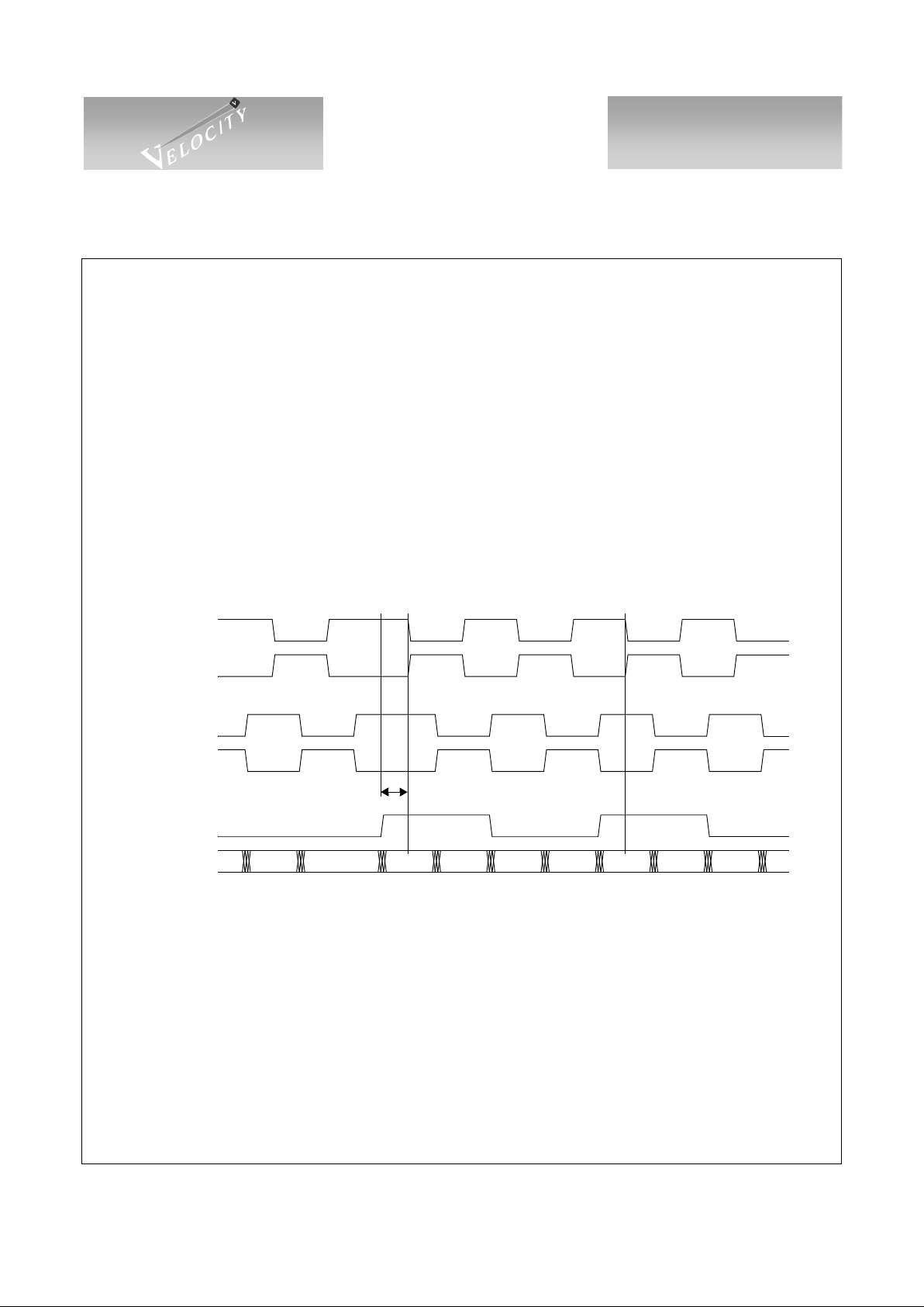
On encountering a comma character, SYNi is driven HIGH. The SYNi pulse is asserted during both 5-bit
halves of the comma character. The SYNi signal is timed identically to data so that it can be captured by the
adjoining protocol logi c al ong with RXi(0:4). Functional wavef or ms for synchronization are shown in Figure 2.
The first K28.5 shows the case where the comma is detected, but it is misaligned so a change in the output data
alignment is required. N ote that one or two half-characters prior to the co mma cha racter may b e corru pted by
the realignment pro cess, but th e comma ch aracter is alw ays recei ved and outp ut correct ly. The second K28.5
shows the case when a comma is detected and no phase adjustment is necessary. It illustrates the position of the
SYNi pulse in relation to the comma character on RXi(0:4).
When RSYN=0, there will always be a rising edge on RCi1 when the first five bits of the K28.5 character
are output. When RSYN=1, there will always be a rising edge on RCi1 between the first and second five bits of
the K28.5 character, and there may or may not be a falling edge on RCi1 coincident with the assertion of SYNi
(the first five bits of the K28.5 character). The behavior depends on the alignment of the new comma relative to
the current RCi(0:1) phase.
Figure 2: Misaligned and Aligned K28.5 Characters
RSYN=0:
Misaligned Comma: Stretched
Aligned Comma: In Phase
Corrupt Corrupt K28.5 (K28.5) A[0:4] K28.5 (K28.5) A[5:9] B[0:4]
RXi[0:4]
SYNi
RCi1
RCi0
RCi1
RCi0
RSYN=1:
VITESSE
SEMICONDUCTOR CORPORATION
Preliminary Data Sheet
VSC7185
Quad Transceiver for
Gigabit Ethernet and Fibre Channel
G52324-0, Rev 3.1 Page 5
03/25/01
© VITESSE SEMICONDUCTOR CORPORATION • 741 Calle Plano • Camarillo, CA 93012
Tel: (800) VITESSE • FAX: (805) 987-5896 • Email: prodinfo@vitesse.com
Internet: www.vitesse.com
Loopback Operation
Loopback operation is controlled by PLUP (Parallel Loopback) and SLPN (Serial Loopback) as shown in
Table 1. When PLUP=0 and SLPN=1 t he part is co nf ig ur ed f or nor mal ope ra ti on . When PLUP =1 and SL PN= 1,
SOi is internally looped to SIi and the SOi outputs are held HIGH. When PLUP=0 and SLPN=0, SIi is looped to
SOi after retiming in the clock recovery unit. Although retiming removes much of the input jitter, the SOi outputs may not meet jitter specifications listed in the “Transmitter AC Specifications” due to low frequen cy jit ter
transfer from SIi to SOi. When PLUP=1 and SLPN=0 (both loopback paths are active) the clock recovery unit
is used to retime the internally looped SO i data. The SIi inputs are looped directly to the SOi outputs without
retiming. Jitter on SOi in this mo de of opera tion will depe nd heavil y on SIi j itter, and again the SOi outputs may
not meet jitter specifications. The remote receiver will see the total jitter accumulation across both the incoming
and outgoing serial links.
Table 1: Loopback Selection
JTAG Access Port
A JT AG acce ss port is provide d to assist in board-level testing . Through t his port most pi ns can be obse rved
or controlled and all TTL outputs can be tri-stated. A full description of the JTAG functions on this device is
available in “VSC7185 JTAG Access Port Functionality.” Circuits designed exclusively for the HDMP-1685A
will automatically disable the JTAG port. Table 7 (Pinout Definitions) in this datasheet shows the proper connections for either HDMP-1685A emulation or for JTAG functionality (in parentheses).
PLUP SLPN Transmitter Source Receiver Source
LOW LOW
Receiver
(Retimed)
Receiver
LOW HIGH Transmitter Receiver
HIGH LOW
Receiver
(Not Retimed)
Transmitter
HIGH HIGH HIGH Transmitter
VITESSE
SEMICONDUCTOR CORPORATION
Preliminary Data Sheet
VSC7185
Quad Transceiver for
Gigabit Ethernet and Fibre Channel
Page 6 G52324-0, Rev 3.1
03/25/01
© VITESSE SEMICONDUCTOR CORPORATION • 741 Ca ll e Pl an o • Camarillo, CA 93012
Tel: (800) VITESSE • FAX: (805) 987-5896 • Email: prodinfo@vitesse.com
Internet: www.vitesse.com
AC Characteristics
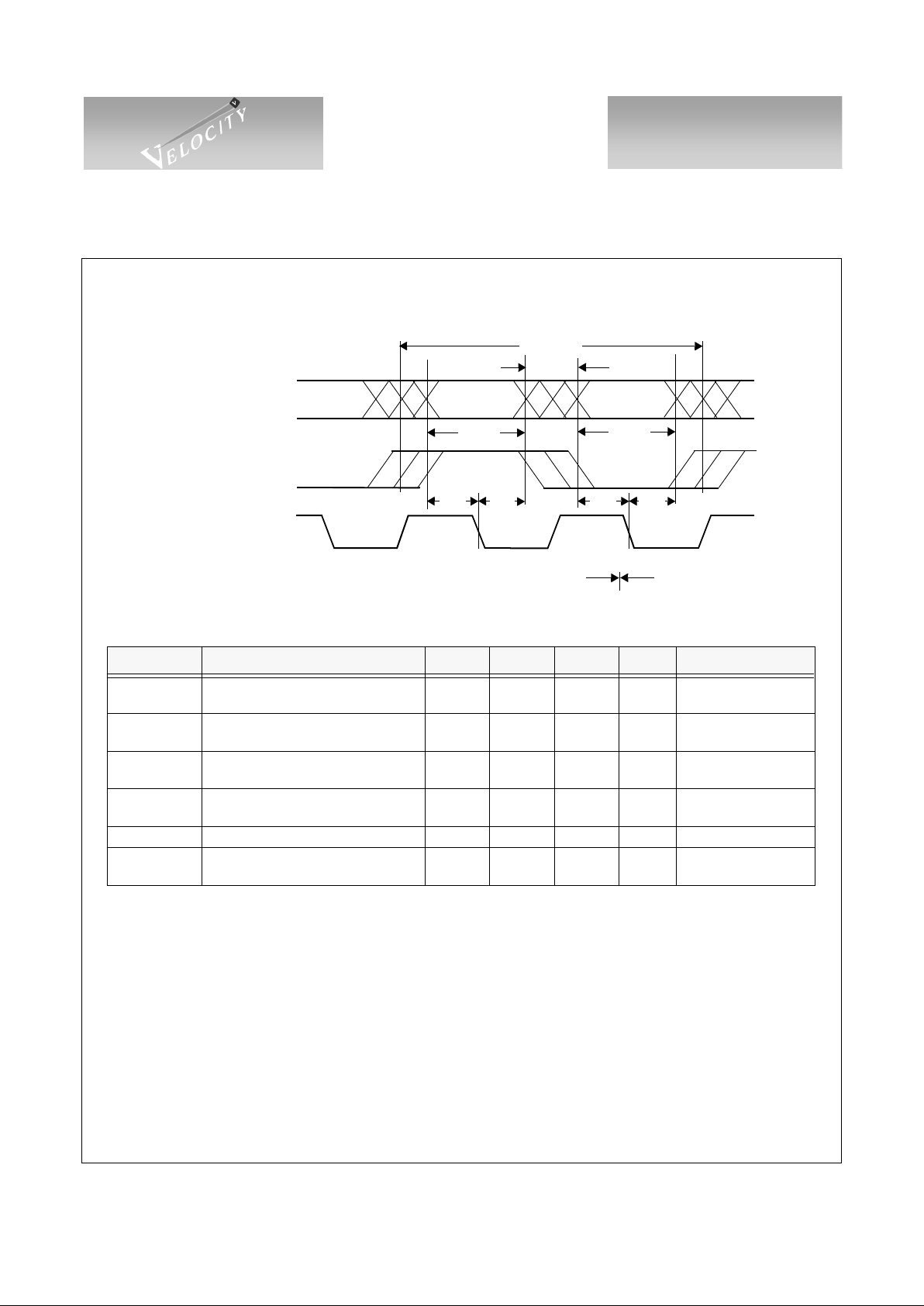
Figure 3: Transmit Timing Waveforms
Table 2: Transmitter AC Characteristics
Parameters Description Min Typ Max Units Conditions
T
TXCT
TXi(0:4) Input Data and TC Clo c k
Transition Range
——2.0 bits
T
TXCV
TXi(0:4) Input Data and TC Clo c k
Valid Time
3.0 ——bits
T
TXS
TXi(0:4) Input Data and TC Set up
Time to Internal 2x Clock
700 ——ps
T
TXH
TXi(0:4) Input Data and TC Ho ld
Time to Internal 2x Clock
700 ——ps
TC Duty Cycle 35 — 65 %
T
TXLAT
Transmitter Latency
11 bits +
1ns
—
11 bits +
2ns
—
Data Valid
TXi(0:4)
TXS TXH
TC
Data Valid
Data Valid
TXCV
TXS TXH
TXCV
TXCT
10 bit times
2x TC
10-BIT CHAR A 10-BIT CHAR B
Internal Clock
 Loading...