

VITESSE
®
Quad Transceiver
SEMICONDUCTOR CORPORATION
Advance Product Information
for Gigabit Ethernet and Fibre Channel
Features
• Four Complete Transmitter/ Receiver Functions
in a Single Integrated Circuit
• Full Fibre Channel (T11) and Gigabit Ethernet
(IEEE 802.3z) Compliance
• 1.05Gb/s to 1.36Gb/s Operation per Channel
• Common or Per-Channel Transmit Byte Clocks
• TTL or PECL Reference Clock Input
• Receiver Squelch Circuit
• Common and Per-Channel, Serial and Parallel
Loopback Controls
• Common Comma Detect Enable Inputs
• Per-Channel Comma Detect Outputs
• Cable Equalization in Receivers
• Replacement For Agilent’s HDMP-1682
• 3.3V Power Supply, 2.67 W Max Dissipation
• 208-Pin, 23mm BGA Packaging
General Description
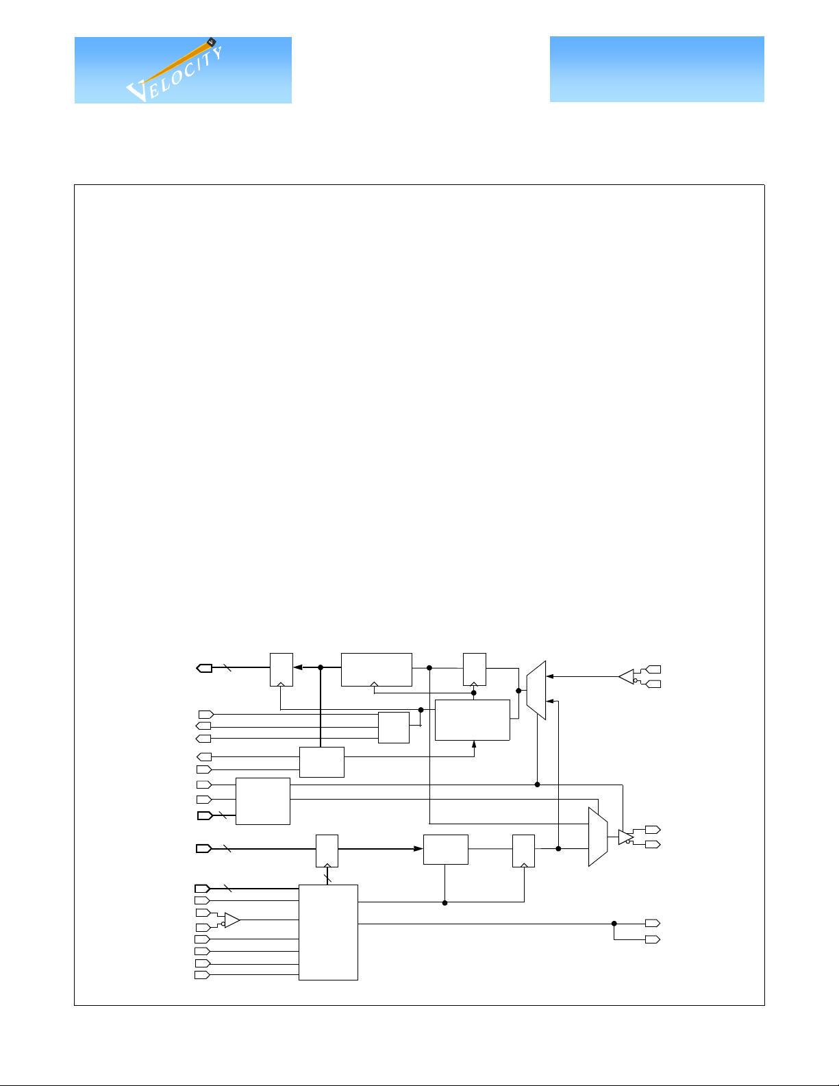
The VSC7182 is a full-speed quad Fibre Channel and Gigabit Ethernet transceiver IC. Each of the four
transmitters has a 10-bit wide bus, running up to 136MHz, which accepts 8B/10B encoded transmit characters
and serializes the data onto high-speed differential outputs at speeds up to 1.36Gb/s. The transmit data can be
synchronous to the reference clock, a common transmit byte clock or a per-channel transmit byte clock. Each
receiver samples serial receive data, recovers the clock and data, deserializes it into 10-bit receive characters,
outputs a recovered clock and detects “Comma” characters. The VSC7182 contains on-chip Phase-Lock Loop
(PLL) circuitry for synthesis of the baud-rate transmit clock and extraction of the clocks from the received serial
streams. The VSC7182 also includes a receiver squelch circuit to control the parallel data bus in the absence of
serial input.
VSC7182 Block Diagram (1 of 4 Channels)
RXi[0:9]
RCM
RCi1
RCi0
SYNi
SYNC
PLUP
SLPN
LPNi
TXi[0:9]
TCi
RFCT
RFC+
RFC-
RFCM
LTCN
CAP0
CAP1
G52307-0, Rev 2.2 Page 1
10/10/00
10
4
10
4
© VITESSE SEMICONDUCTOR CORPORATION • 741 Calle Plano • Camarillo, CA 93012
Q D
Comma
Detect
Loopback
Control
Clock
Multiply
x10/x20
Tel: (800) VITESSE • FAX: (805) 987-5896 • Email: prodinfo@vitesse.com
Q D
4
Unit
Serial to
Parallel
÷
SEL
÷
10/
÷
20
Internet: www.vitesse.com
10
Parallel
to Serial
Q D
Clock
Recovery
0
1
0
D QD Q
1
SI+
SI-
SO+
SO-
RFCO0
RFCO1
VITESSE
®
VSC7182
SEMICONDUCTOR CORPORATION
Quad Transceiver
Advance Product Information
for Gigabit Ethernet and Fibre Channel
Functional Description
Notation
In this document, each of the four channels are identified as Channel A, B, C or D. When discussing a signal on any specific channel, the signal will have the Channel letter embedded in the name, for example,
“TA[0:9]”. When referring to the common behavior of a signal which is used on each of the four channels, a
lower case “x” is used in the signal name, i.e. TXi[0:9]. Differential signals, such as RA+ and RA-, may be
referred to as a single signal, i.e. RA, by dropping reference to the “+” and “-”. “RFC” refers to either the TTL
input RFCT, or the PECL differential inputs RFC+/RFC-, whichever is used.
Clock Synthesizer
The VSC7182 clock synthesizer multiplies the reference frequency provided on the RFC input by 10 or 20
to achieve a baud rate clock between 1.05GHz and 1.36GHz. The RFC input can be either TTL or PECL. If
TTL, connect the TTL input clock to RFCT. If PECL, connect the PECL inputs to RFC+ and RFC-. The internal clock presented to the clock synthesizer is a logical XNOR of RFCT and RFC+/-. The reference clock will
be active HIGH if the unused input is HIGH. The reference clock is active LOW if the unused input is LOW.
RFCT has an internal pull-up resistor. Internal biasing resistors set the proper DC level on RFC+/- so AC-coupling may be used.
The TTL outputs, RFCO0 and RFCO1, provide a clock that is frequency-locked to the RFC input. This
clock is derived from the clock synthesizer and is always 1/10th the baud rate, regardless of the state of the
RFCM input.
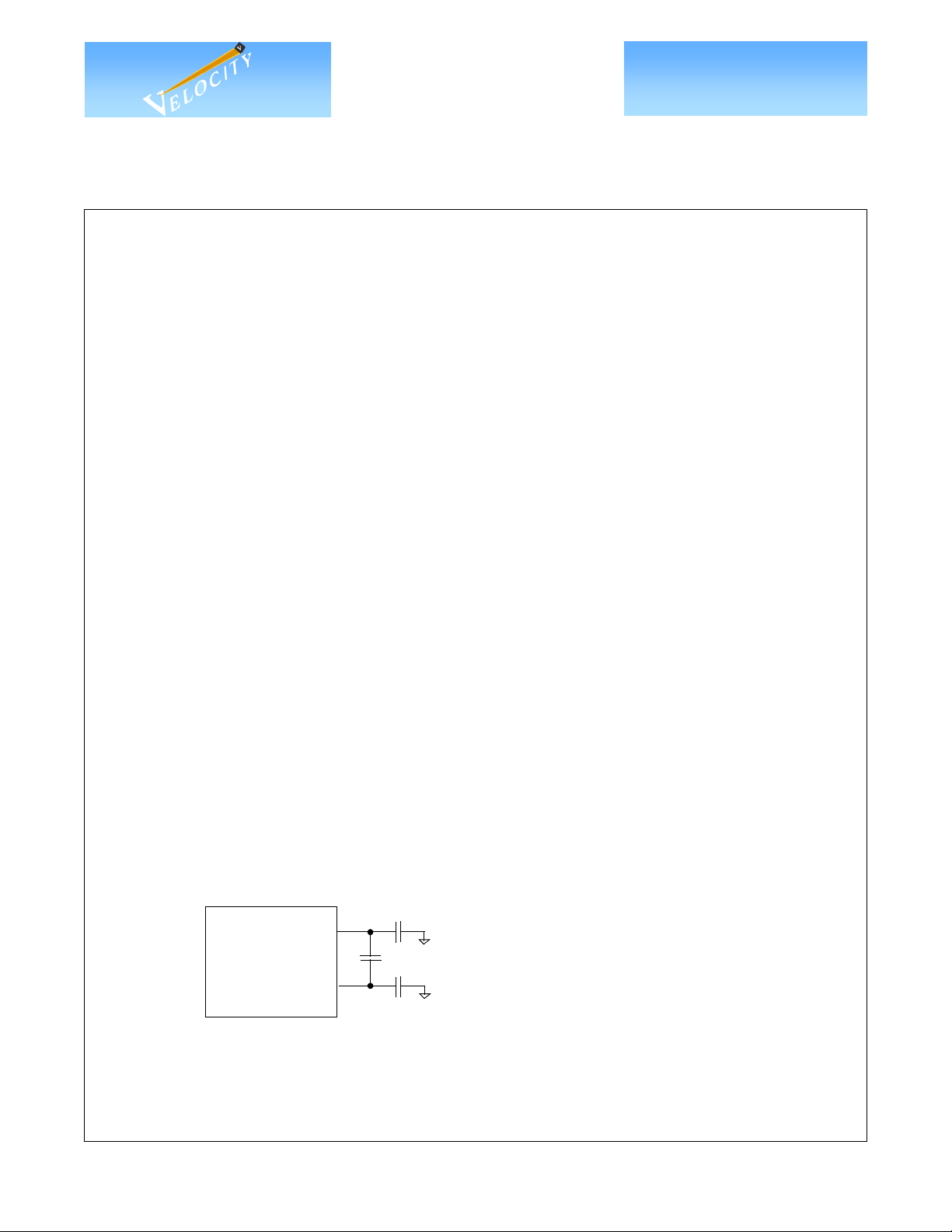
The on-chip PLL uses a single external 0.1µF capacitor, connected between CAP0 and CAP1, to control the
loop filter. This capacitor should be a multilayer ceramic dielectric, or better, with at least a 5V working voltage
rating and a good temperature coefficient (NPO is preferred but X7R may be acceptable). These capacitors are
used to minimize the impact of common-mode noise on the Clock Multiplier Unit (CMU), especially power
supply noise. Higher value capacitors provide better robustness in systems. NPO is preferred because if an X7R
capacitor is used, the power supply noise sensitivity will vary with temperature.
For best noise immunity, the designer may use a three capacitor circuit with one differential capacitor
between CAP0 and CAP1, C1, a capacitor from CAP0 to ground, C2, and a capacitor from CAP1 to ground,
C3. Larger values are better but 0.1µF is adequate. However, if the designer cannot use a three capacitor
circuit, a single differential capacitor, C1, is adequate. These components should be isolated from noisy traces.
Figure 1: Loop Filter Capacitors (Best Circuit)
VSC7182
Page 2 G52307-0, Rev 2.2
© VITESSE SEMICONDUCTOR CORPORATION • 741 Calle Plano • Camarillo, CA 93012
CAP0
C1
CAP1
Tel: (800) VITESSE • FAX: (805) 987-5896 • Email: prodinfo@vitesse.com
C2
C3
Internet: www.vitesse.com
C1=C2=C3= >0.1µF
MultiLayer Ceramic
Surface Mount
NPO (Preferred) or X7R
5V Working Voltage Rating
10/10/00
VITESSE
®
Quad Transceiver
SEMICONDUCTOR CORPORATION
Advance Product Information
for Gigabit Ethernet and Fibre Channel
Serializer
The VSC7182 accepts TTL input data as a parallel 10-bit character on the TXi[0:9] bus which is latched
into the input register on the rising edge of either RFC or TCi. Three clocking modes are available and automatically detected by the VSC7182. If TCC is static and RFCM is HIGH, then all four TXi[0:9] busses are latched
on the rising edges of RFC. If TCC is static and RFCM is LOW, then RFC is multiplied by 20 and the input busses are latched on the rising edges of RFC and at the midpoint between rising edges. If TCC is toggling but TCB
is static, then all four TXi[0:9] busses are latched on the rising edges of TCC. If TCB and TCC are both toggling
then the rising edge of each TCi latches the corresponding TXi[0:9] bus.
The active TCC or TCi inputs must be frequency-locked to RFC. There is no specified phase relationship.
Prior to normal data transmission, LTCN must be asserted LOW so the VSC7182 can lock to TCi, which may
result in corrupted data being transmitted. Once LTCN has been raised HIGH, the transmitters remain locked to
RFC and can tolerate +/-2 bit times of drift in TCi relative to RFC.
The 10-bit parallel transmission character will be serialized and transmitted on the TXi PECL differential
outputs at the baud rate with bit TXi0 (bit A) transmitted first. User data should be encoded using 8B/10B or an
equivalent code. The mapping to 10B encoded bit nomenclature and transmission order is illustrated below,
along with the recognized comma pattern.
Table 1: Transmission Order and Mapping of a 10B Character
Data Bit TXi9 TXi8 TXi7 TXi6 TXi5 TXi4 TXi3 TXi2 TXi1 TXi0
10B Bit Position j h g f i e d c b a
Comma Character x x x 1 1 1 1 1 0 0
Clock Recovery
The VSC7182 accepts differential high-speed serial input from the selected source (either the PECL SI+/
SI- pins or the internal TXi+/- data), extracts the clock and retimes the data. Equalizers are included in the
receiver to open the data eye and compensate for InterSymbol Interference (ISI) which may be present in the
incoming data. The serial bit stream should be encoded so as to provide DC balance and limited run length by
an 8B/10B encoding scheme. The digital Clock Recovery Unit (CRU) is completely monolithic and requires no
external components. For proper operation, the baud rate of the data stream to be recovered should be within
+200 ppm of ten times the RFC frequency. For example, Gigabit Ethernet systems would use 125MHz oscillators with a +100ppm accuracy resulting in +200 ppm between VSC7182 pairs.
Deserializer
The recovered serial bit stream is converted into a 10-bit parallel output character. The VSC7182 provides
complementary TTL recovered clocks, RCi0 and RCi1, which are at 1/20th of the serial baud rate (if
RCM=LOW) or 1/10th (if RCM=HIGH). The clocks are generated by dividing down the high-speed recovered
clock which is phase-locked to the serial data. The serial data is retimed, deserialized and output on RXi[0:9].
If serial input data is not present, or does not meet the required baud rate, the VSC7182 will continue to
produce a recovered clock so that downstream logic may continue to function. The RCi0/RCi1 output frequency
under these circumstances will differ from its expected frequency by no more than +1%. A receiver squelch circuit forces the parallel data output bus to all ones if the serial receiver input level is less than 100mV differential
peak-to-peak.
G52307-0, Rev 2.2 Page 3
10/10/00
© VITESSE SEMICONDUCTOR CORPORATION • 741 Calle Plano • Camarillo, CA 93012
Tel: (800) VITESSE • FAX: (805) 987-5896 • Email: prodinfo@vitesse.com
Internet: www.vitesse.com
VITESSE
®
VSC7182
SEMICONDUCTOR CORPORATION
Quad Transceiver
Advance Product Information
for Gigabit Ethernet and Fibre Channel
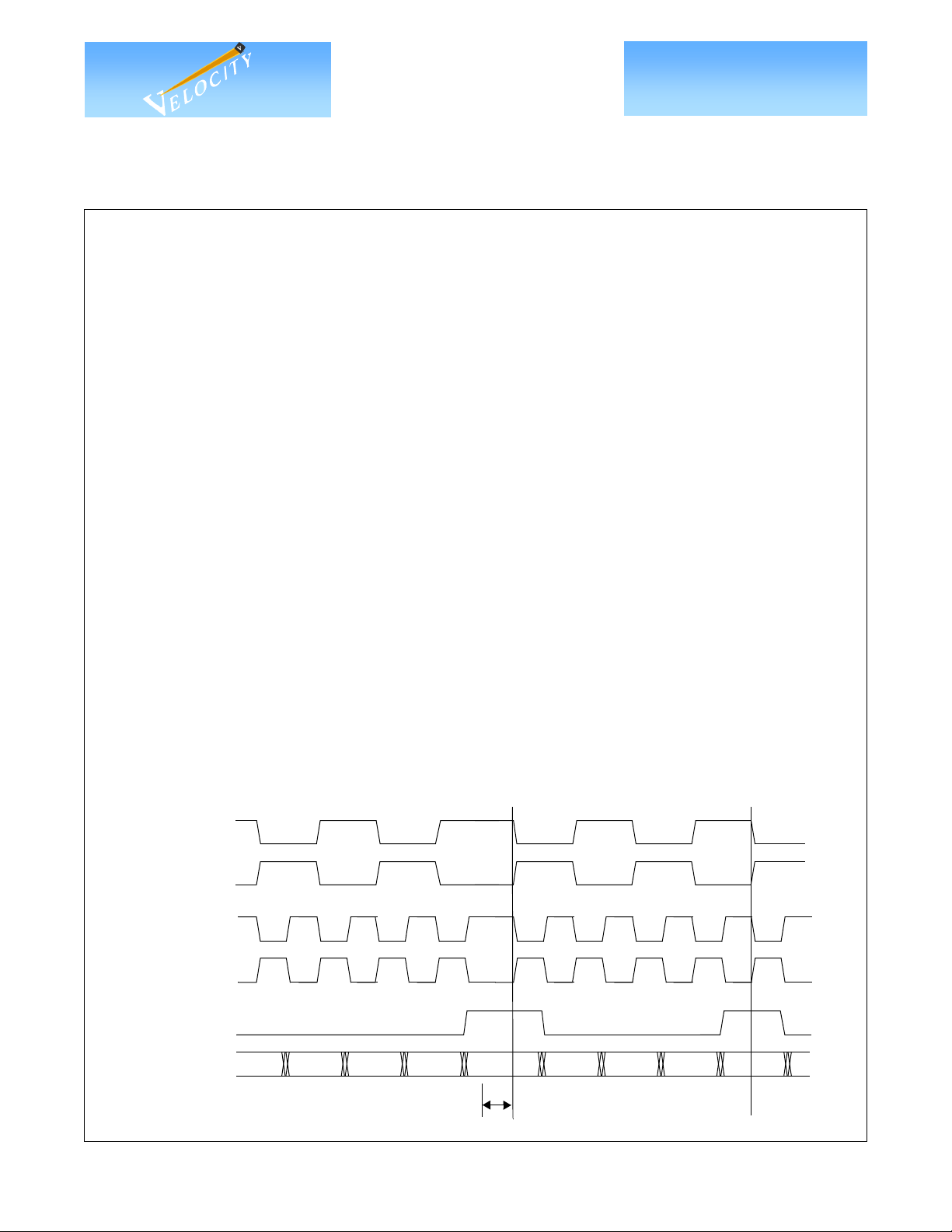
Word Alignment
The VSC7182 provides 7-bit comma character recognition and data word alignment. Word synchronization
is enabled on all channels by asserting SYNC HIGH. When synchronization is enabled, the receiver examines
the recovered serial data for the presence of the “Comma” pattern. This pattern is “0011111XXX”, where the
leading zero corresponds to the first bit received. The comma sequence is not contained in any normal 8B/10B
coded data character or pair of adjacent characters. It occurs only within special characters, known as K28.1,
K28.5 and K28.7, which are defined for synchronization purposes. Improper comma alignment is defined as
any of the following conditions:
1) The comma is not aligned within the 10-bit transmission character such that RXi(0...6) = “0011111.”
2) The comma straddles the boundary between two 10-bit transmission characters.
3) The comma is properly aligned but occurs in the received character presented during the rising edge of
RCi0 rather than RCi1.
When SYNC is HIGH and an improperly aligned comma is encountered, the recovered clock is stretched,
never slivered, so that the comma character and recovered clocks are aligned properly to RXi[0:9]. This results
in proper character and word alignment. When the parallel data alignment changes in response to a improperly
aligned comma pattern, data which would have been presented on the parallel output port prior to the comma
character, and possibly the comma character itself, may be lost. Possible loss of the comma character is data
dependent, according to the relative change in alignment. Data subsequent to the comma character will always
be output correctly and properly aligned. When SYNC is LOW, the current alignment of the serial data is maintained indefinitely, regardless of data pattern.
On encountering a comma character, SYNi is driven HIGH. The SYNi pulse is presented simultaneously
with the comma character and has a duration equal to the data. The SYNi signal is timed such that it can be captured by the adjoining protocol logic on the rising edge of RCi1. Functional waveforms for synchronization are
given in Figure 2. The first K28.5 shows the case where the comma is detected, but it is misaligned so a change
in the output data alignment is required. Note that up to three characters prior to the comma character may be
corrupted by the realignment process. The second K28.5 shows the case when a comma is detected and no
phase adjustment is necessary. It illustrates the position of the SYNi pulse in relation to the comma character on
RXi[0:9].
Figure 2: Misaligned and Aligned K28.5 Characters
RCi0
(RCM LOW)
RCi1
RCi0
([RCM HIGH)
RCi1
SYNi
RXi[0:9]
Page 4 G52307-0, Rev 2.2
© VITESSE SEMICONDUCTOR CORPORATION • 741 Calle Plano • Camarillo, CA 93012
Corrupt Corrupt Corrupt
Misaligned Comma: Stretched
Tel: (800) VITESSE • FAX: (805) 987-5896 • Email: prodinfo@vitesse.com
Internet: www.vitesse.com
K28.5
Data1 Data2 Data3
K28.5Data
Aligned Comma
10/10/00
VITESSE
®
Quad Transceiver
SEMICONDUCTOR CORPORATION
Advance Product Information
for Gigabit Ethernet and Fibre Channel
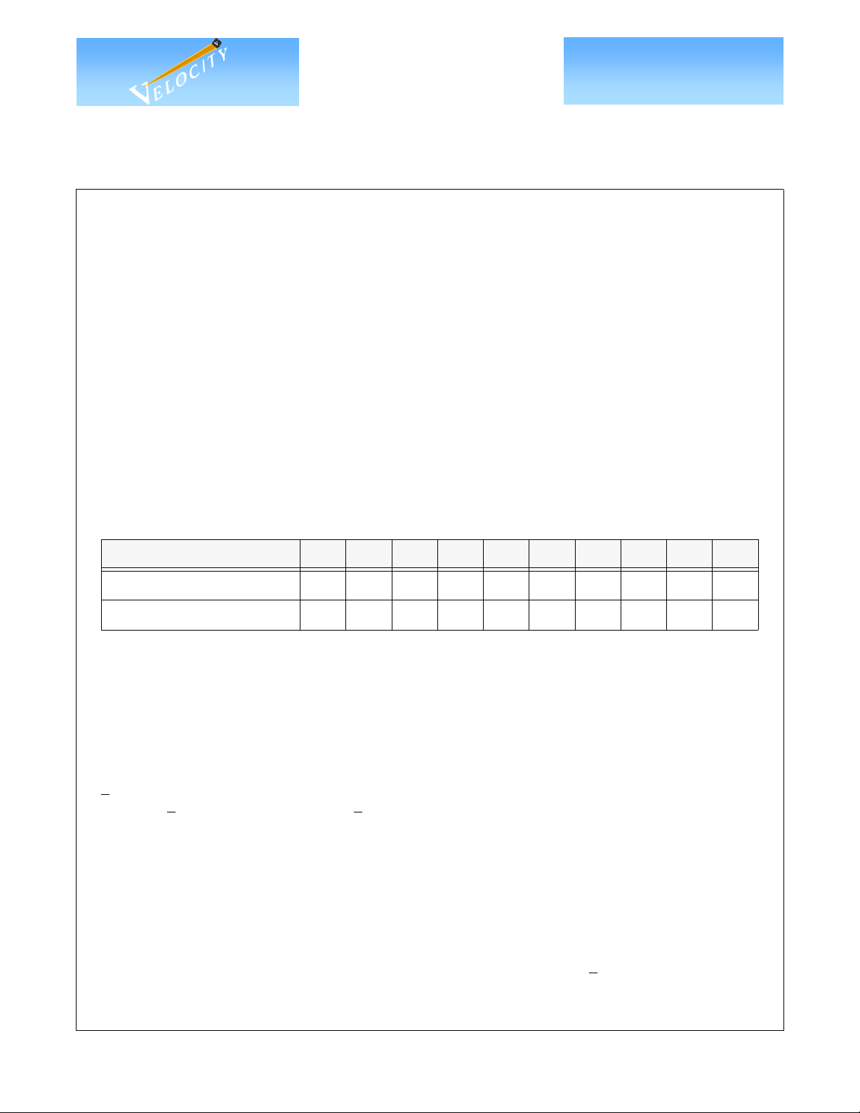
Loopback Operation
Loopback operation is controlled by the PLUP (Parallel Loopback), SLPN (Serial Loopback) and LPNi
inputs as shown in Table 2. LPNi enables PLUP/SLPN on a per-channel basis when LOW. If LPNi is HIGH,
PLUP/SLPN have no impact on Channel x. When SLPN and PLUP are both HIGH the transmitter output is
held HIGH. When RXx is looped back to TXx, the data goes through a clock recovery unit so much of the
input jitter is removed. However, the TXx outputs may not meet jitter specifications listed in the “Transmitter
AC Specifications” due to low frequency jitter transfer from RXx to TXx.
Table 2: Loopback Selection
LPNi PLUP SLPN Tranmitter Source Receiver Source
LOW LOW LOW Receiver Receiver
LOW LOW HIGH Transmitter Receiver
LOW HIGH LOW Transmitter Transmitter
LOW HIGH HIGH HIGH Transmitter
HIGH X X Transmitter Receiver
JTAG Access Port
A JTAG Access Port is provided to assist in board-level testing. Through this port most pins can be
accessed or controlled and all TTL outputs can be tri-stated. A full description of the JTAG functions on this
device is available in “VSC7182 JTAG Access Port Functionality.”
G52307-0, Rev 2.2 Page 5
10/10/00
© VITESSE SEMICONDUCTOR CORPORATION • 741 Calle Plano • Camarillo, CA 93012
Tel: (800) VITESSE • FAX: (805) 987-5896 • Email: prodinfo@vitesse.com
Internet: www.vitesse.com
VITESSE
®
VSC7182
SEMICONDUCTOR CORPORATION
Quad Transceiver
for Gigabit Ethernet and Fibre Channel
AC Characteristics
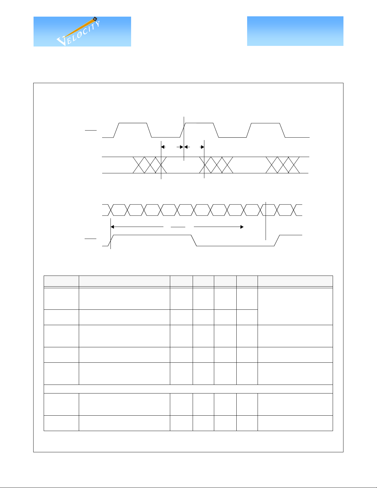
Figure 3: Transmit Timing Waveforms
RFC
TCi
TXi[0:9]
10-Bit Data
+/-TXi
RFC
TCi
Data Valid
T
1
Data Valid
T
RLAT
T
TLAT
Advance Product Information
T
2
Data Valid
TXi0 TXi1 TXi2
Table 3: Transmitter AC Characteristics
Parameter Description Min Typ Max Units Conditions
T
1
T
2
T
SDR,TSDF
T
RLAT
T
TLAT
RJ Random jitter (rms) — 5 8 ps
DJ
TXi[0:9] setup time to the rising edge
of TCi or RFC
TXi[0:9] hold time after the rising
edge of TCi or RFC
TXi+/TXi- rise and fall time — — 300 ps
Latency from rising edge of RFC to
TXi0 appearing on TX+/TX-
Latency from rising edge of TCi to
TXi0 appearing on TX+/TX-
Transmitter Output Jitter
Serial data output deterministic jitter
(pk-pk)
1.5 — — ns
1.0 — — ns
7bc +
0.66ns
5bc +
0.66ns
— 35 80 ps
—
—
7bc +
1.46ns
11bc
+
1.46ns
Measured between the valid
data level of TXi[0:9] to the
1.4V point of TCi or RFC
20% to 80%, 75Ω load to
VDD/2, tested on a sample
basis
bc = bit clocks
ns = nanoseconds
bc = bit clocks
ns
ns = nanoseconds
Measured at SO+/-, 1 sigma
deviation of 50% crossing
point
IEEE 802.3Z Clause 38.68,
tested on a sample basis
Page 6 G52307-0, Rev 2.2
© VITESSE SEMICONDUCTOR CORPORATION • 741 Calle Plano • Camarillo, CA 93012
Tel: (800) VITESSE • FAX: (805) 987-5896 • Email: prodinfo@vitesse.com
Internet: www.vitesse.com
10/10/00
 Loading...