

VITESSE VSC7148 Datasheet
VITESSE
SEMICONDUCTOR CORPORATION
•
All the functionality needed to implement a com-
• Configurable as either a single 16-drive loop or
Product Brief
16-Port JBOD Loop Chip for
1.0625 Gb/s FC-AL Storage Applications
Features
plete daisy-chainable 16-drive 1Gb/s FC-AL JBOD
Subsystem
• Two host ports with two pairs of FibreTimerTM
Clock Recovery Units (CRUs) configurable as
either Repeaters or Retimers
• Sixteen Port Bypass Circuits (PBC) for drive control
• Sixteen PBC internal Snoop LoopTM for loop diagnostics
two 8-drive loops
• I2C interface for configuration/status/control
• Seamless interface to Enclosure Management
Chipsets such as the Vitesse SSC100/VSC055
for managed JBOD applications
• On-chip terminators selectable as 100/150 ohm
• 3.3V Power Supply, 4.3 W
• 256-pin, 27mm Thermally Enhanced BGA
Applications
The VSC7148 contains all the functions needed to implement an entire daisy-chainable 1.0625 Gb/s FC-AL
JBOD Loop for storage systems containing up to sixteen disk drives. This device is typically used in distributing Fibre Channel signals to an array of disk drives in managed and un-managed arrays. The use of an I2C
Interface allows access to status information and control of configuration through an easily-implemented,
industry-standard, protocol.
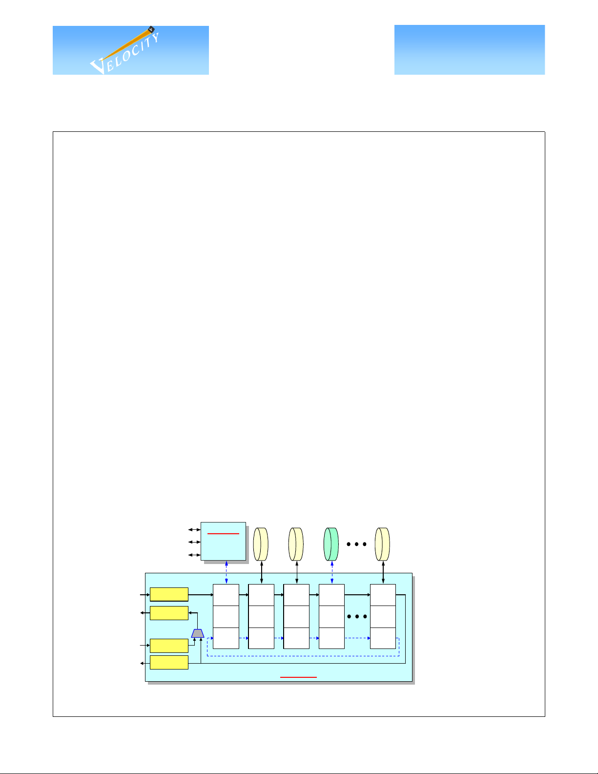
The VSC7148 easily interfaces with the SSC100 Enclosure Management Controller to offer unsurpassed
diagnostic capability within the industry (refer to Figure 1). The SSC100 communicates with the VSC7148
through the I2C interface to provide complete loop status, configuration, and diagnostic control to the host. In
this configuration, up to fifteen drives on a single loop may be accessed with a single Fibre Channel connector.
Serial data from the loop enters the FC-AL port of the SSC100 where the data is processed, returned to the loop,
and handed to the VSC7148 for drive communications. In addition, the VSC7148 is the only device on the market that supports two loops within a single device. The External Loop may be configured for all Fibre Channel
data traffic while the Snoop Loop may be used for monitoring or isolating specific ports for diagnostics. With
this architecture, a design engineer has the flexibility to offer full Fibre Channel support on the External Loop
IPMI
RS-232
Ethernet
Host
Port #1
Host
Port #2
Repeater
Retimer
(4) FibreTimer
Circuits
Repeater
Retimer
TM
Figure 1. Managed JBOD Using the VSC7148 and SSC100
Rev. 1.0
5/25/00 741 Calle Plano, Camarillo, CA 93012 • 805/388-3700 • FAX: 805/987-5896
SSC100
SSC100
Enclosure
Enclosure
Management
Management
Controller
Controller
External
Loop
PBC 0
Snoop
Loop
VITESSE SEMICONDUCTOR CORPORATION Page 1
Drive 1
External
Loop
PBC 1
Snoop
Loop
Drive 2
External
Loop
PBC 2
Snoop
Loop
Drive 3
External
Loop
PBC 3
Snoop
Loop
Drive 15
External
Loop
PBC 15
Snoop
Loop
VSC7148 16-Port JBOD Loop Chip
For diagnostic testing,
the SSC100 initiates
communication with
an individual drive
(e.g. Drive 3) via the
VSC7148 Snoop
LoopTM while all other
drives are fully
accessible to the Fibre
Channel loop.
VITESSE
Product Brief
VSC7148
SEMICONDUCTOR CORPORATION
16-Port JBOD Loop Chip for
1.0625 Gb/s FC-AL Storage Applications
while isolating error conditions and performing loop diagnostics on the Snoop Loop. When coupled with the
SSC100's initiator features, the VSC7148 can provide fault isolation conditions and JBOD quality characteristics back to the host in real-time. When used in a managed JBOD application, the VSC7148/SSC100 chipset
allows fault isolation down to the lowest Field Replaceable Unit (FRU) to reduce downtime and support costs,
and lead to higher availability.
General Description
Along with the sixteen PBCs, four FibreTimer digital Clock Recovery Units (CRUs) can be configured as
Repeaters or Retimers. Repeaters, which attenuate jitter, are normally located at the input to the loop and
retransmit recovered data synchronously to the recovered clock. Retimers, which eliminate jitter transfer, are
normally located at the outputs of the loop and retransmit data synchronously to the reference clock in order to
provide complete Fibre Channel jitter compliance at the output.
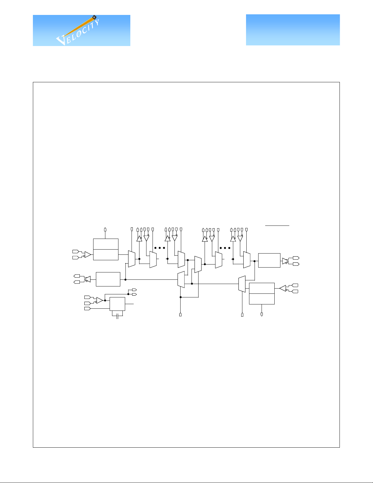
MUX4
1
0
2
C Interface)
I8+
I8-
O8+
O8-
P8
1
0
PBC8
OF+
PBCF
MUX2
PF
CDR3(R)
SDU3
NOT SHOWN:
Two-Wire Interface
Signal Detection
JTAG
INT#
CDR2(T)
0
SD3
SO2+
SO2-
PORT2
SI2+
SI2-
IF+
IF-
OF-
1
0
0
1
VSC7148 Block Diagram (When not using the I
DRIVE 0 DRIVE 7 DRIVE 8 DRIVE 15
I7+
I7-
O7+
O7-
P7
1
0
PBC7
0
1
MUX3
S/D M2
SI1+
SI1-
PORT1
SO1+
SO1-
REFI+
REFI-
HALF/FULL
SD0
SDU0
CDR0(R)
MUX1
CDR1(T)
53.125/106.25MHz
CMU
CAP0 CAP1
0.1uF
M1
1
0
1.0625 GHz
O0+
O0-
PBC0
REFO0
REFO1
I0+
I0-
P0
1
0
Software
The VSC7148 is supported by an API within our enclosure management Software Development Kit
(SDK). The SDK includes software to implement a FC transport and SES diagnostic environment. In addition,
the SDK also includes a System Services module which provides APIs to the peripheral functionality (interrupts, timers etc.) in the Enclosure Management Controller. The System Services also includes driver libraries
for popular I2C devices such as National's LM75, LM78, and many others.
For More Information: www.vitesse.com or email: prodinfo@vitesse.com or TEL: 1-800-VITESSE
Notice: Vitesse Semiconductor Corporation reserves the right to make changes in its products, specifications or other information at any time without
prior notice. Therefore the reader is cautioned to confirm that this Product Brief is current prior to placing any orders. The company assumes no responsibility for any circuitry described other than circuitry entirely embodied in the Vitesse product. Please contact Vitesse Semiconductor to obtain the latest
product status and most recent specification for this product.
Warning: Vitesse Semiconductor Corporation’s product are not intended for use in life support appliances, devices or systems. Use of a Vitesse prod-
uct in such applications without the written consent is prohibited.
Page 2 VITESSE SEMICONDUCTOR CORPORATION
Rev. 1.0
741 Calle Plano, Camarillo, CA 93012 • 805/388-3700 • FAX: 805/987-5896 5/25/00
 Loading...