

VITESSE VSC7146RH Datasheet

VITESSE
SEMICONDUCTOR CORPORATION
Advance Product Information
VSC7146
2.5Gb/s, 20-Bit Tr ansceiver
Features
• Speed Selectable Full-Duplex Transceiver:
- 1.06/2.12Gb/s for FibreChannel
- 1.25/2.5Gb/s for Gigabit Ethernet
• 20-Bit TTL Interface for Transmit and
Receive Data at 125MHz
• Monolithic Clock Synthesis and Clock
Recovery - No External Components
• 125MHz TTL Reference Clock
• Automatic Lock-to-R eference Function
• Suitable for Both Coaxi al and O pt i cal Link Applications
• Low Power Operation: 2.5 W max
• 80-Pin, 14mm Thermally-Enhanced EDQUAD
Package
• Single +3.3V Supply
General Description
The VSC7146 is a 2.5Gb/s Transceiver optimized for ease-of-use and efficiency in high-performance data
transmission systems. The VSC7146 accepts two 10-bit 8b/10b encoded transmit characters, latches them on
the rising edge of Transmit Byte Clock (TBC) and serializes the data onto the TX+/- differential outputs at a
baud rate, which is 20 times the TBC frequency. The VSC7146 also samples serial receive data on the RX+/differential inputs, recovers the clock and data, deserializes it onto two 10-bit receive characters, outputs a
recovered clocks at one-twentieth of the incoming baud rate and detects Fibre Channel “comma” characters.
The VSC7146 contai ns o n- ch ip Ph ase -Lo ck Loop (PLL ) c ircu itr y for sy nth esis o f th e bau d -rate tra nsm it cloc k,
and extraction of the clock from the received serial stream. These circuits are fully monolithic and require no
external components.
Block Diagram
EWRAP
20
R0:19
RBC
RBCN
COM_DET
EN_CDET
T0:19
TBC
REF
TXRATE
BCMN
Q D
125 MHz
20
125 MHz
Frame
Logic
D Q
Serial to
Parallel
÷
20
Comma
Detect
Parallel
to Serial
PLL Clock
Multiply (x20)
Retimed
Data
Recovered
Clock
2.5 Gb/s
Serial Data
2.5 GHz
Synthesized
Clock
Q D
Clock
Recovery
2:1
D Q
2.5 Gb/s
RX+
RX-
RXRATE
TX+
TX-
G52162-0, Rev. 2.7
8/28/00 741 Calle Plano, Camarillo, CA 93012 • 805/388-3700 • FAX: 805/987-5896
VITESSE SEMICONDUCTOR CORPORATION
Page 1

VITESSE
SEMICONDUCTOR CORPORATION
2.5Gb/s, 20-Bit Transceiver
Advance Product Information
VSC7146
Functional Description
Clock Synthesizer
The VSC7146 clock synthesizer multiplies the 125MHz reference frequency provided on the REF input by
20 to achieve a baud rate clock at 2.5GHz. The clock synthesizer contains a fully monolithic PLL which
requires no external components. An additional 125MHz clock, TBC, should be provided to clock in the data
bus. Since TBC is only used for the purpose of clocking data in, it is not required to have the same jitter
constraints as REF. REF clock and TBC should preserve certain phase margins and be of the same frequency.
Serializer
The VSC7146 accepts TTL input data as two parallel 10-bit characters on the T[0:19] bus which is latched
into the input latch on the rising edge of a 125MHz clock at TBC. This data will be serialized and transmitted on
the TX differential outputs at a baud rate of 20 times the frequency of the TBC input, with bit T0 transmitted
first. User data should be enco ded f or t ra nsmissi on us in g th e 8B/ 10B block code described in th e Fi br e Ch annel
specification, or an equivalent, edge rich, DC-balanced code. If EWRAP is HIGH, the transmitter will be
disabled with TX+ HIGH and TX- LOW. If EWRAP is LOW, the transmitter outputs serialized data. The
phases of REF clock and TBC can be identical, but there is a phase relationship between the two input clocks
which must be maintained.
Transmission Character Interface
In Fibre Channel, an encoded byte is 10 bits and is referred to as a transmission character. The 20-bit
interface on the VSC7146 corresponds to two transmission characters. This mapping is shown in Figure 1.
Figure 1: Transmission Order and Mapping to Fibre Channel Character
Parallel Data Bits 19 18 17 16 15 14 13 12 11 10 09 08 07 06 05 04 03 02 01 00
8B/10B Bit Position j h g f i e d c b a j h g f i e d c b a
V alid “Comma” Position 1111100
Last Data Bit Transm itted
Clock Recovery
The VSC7146 accepts different ial hi gh-spe ed seri al inpu ts o n th e RX+/RX- pins, (when E WRAP is LOW),
extracts the clock and retimes t he dat a. The serial bit stream shoul d be encoded so as to provide DC b ala nce a nd
limited run length by a Fibre Channel-compatible 8B/10B transmitter or equivalent. The VSC7146 clock
recovery circuitry is completely monolithic and requires no external components. For proper operation, the
baud rate of the data stream to be recovered should be within 200ppm of twenty times the REF frequency. This
allows oscillators on either end of the link to be 125MHz +/- 100ppm.
First Data Bit Transmitted
Page 2
741 Calle Plano, Camarillo, CA 93012 • 805/388-3700 • FAX: 805/987-5896 8/28/00
VITESSE SEMICONDUCTOR CORPORATION
G52162-0 Rev. 2.7

VITESSE
SEMICONDUCTOR CORPORATION
Advance Product Information
VSC7146
Deserializer
The retimed serial bit stream is converted into two 10-bit parallel out put characters. The VSC7146 provides
a TTL recovered clock, RBC, at one twentieth of the serial baud rate. The clock is generated by dividing down
the high-speed clock which is phase-locked to the serial data. The serial data is retimed by the internal highspeed clock, and deseriali zed. The resul ting par allel dat a will be cap ture d by the adjo ining proto col logic on t he
rising edge of RBC.
If serial input data is not present, or does not meet the required baud rate, the VSC7146 will continue to
produce a recovered clock and RBC will automatically lock to the REF reference clock. This eliminates the
need for a Lock-to-Reference input pin and simplifies the support software for that function.
Word Alignment
The VSC7146 provides 7-bit Fibre Chan nel “comma” charact er recognition and dat a word al ignment. Word
synchronization is enabled by asserting EN_CDET HIGH. When synchronization is enabled, the VSC7146
constantly examines the serial data for the presence of the Fibre Channel “comma” character. This pattern is
“0011111XXX”, where the leading zero corresponds to the first bit received. The “comma” sequence is not
contained in any normal 8B/10B coded data character or pair of adjacent characters. It occurs only within
special characters, known as K28.1, K28.5 and K28.7, which are defined specifically for synchronization in
Fibre Channel systems. Improper alignment of the “comma” character is defined as either of the following
conditions:
2.5Gb/s, 20-Bit Tr ansceiver
1) The “comma” is not aligned within the 10-bit transmission character such that T0...T6 = “0011111.”
2) The “comma” straddles the boundary between two 10-bit transmission characters.
When EN_CDET is HIGH and an improperly aligned “comma” is encountered, the internal data is shifted
in such a manner that the “comma” character is aligned properly in R[0:6] as shown in Figure 1. This results in
proper character and word alignment. When the parallel data alignment changes in response to a improperly
aligned “comma” pattern, some data which would have been presented on the parallel output port may be lost.
However, the synchronization character and subsequent data will be output correctly and properly aligned.
When EN_CDET is L OW, the current alignme nt o f th e seri al d ata is mai nt ain ed i nde fini te ly, regardless of data
pattern.
On encountering a “comma” character, COM_DET is driven HIGH to inform the user that realignment of
the parallel data field may have occurred. The COM_DET pulse is presented simultaneously with the “comma”
character and has a duration equal t o the data. Th e COM_DET signal is timed such t hat it can be captured b y the
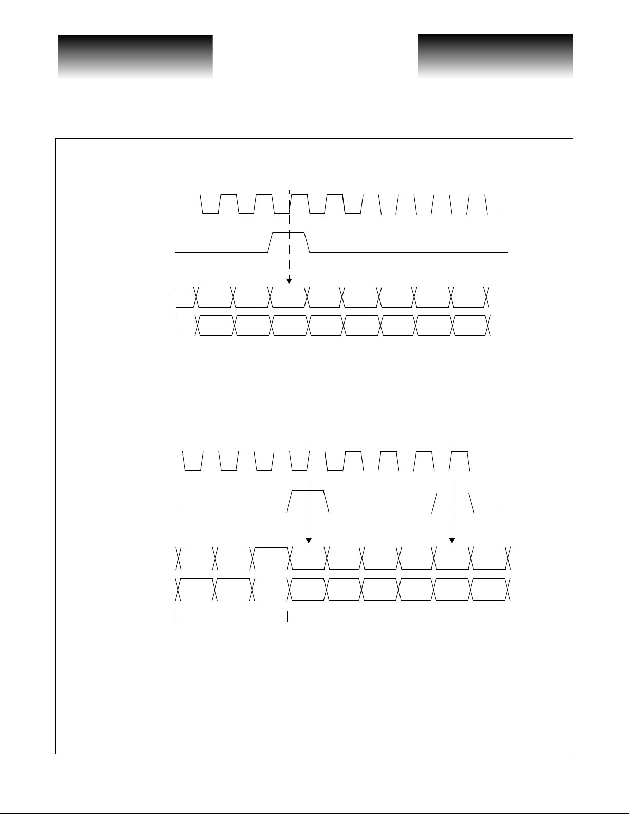
adjoining protocol logic on the rising edge of RBC. Functional waveforms for synchronization are shown in
Figure 2 and Figure 3. Figure 2 shows the case when a “comma” character is detected and no phase adjustment
is necessary. It illustrates the position of the COM_DET pulse in relation to the “comma” character on R[0:6].
Figure 3 shows the case where the K28.5 is detected, but it is out-of-phase and a change in the output data
alignment is required. Note that up to three characters prior to the “comma” character may be corrupted by the
realignment process.
G52162-0, Rev. 2.7
8/28/00 741 Calle Plano, Camarillo, CA 93012 • 805/388-3700 • FAX: 805/987-5896
VITESSE SEMICONDUCTOR CORPORATION
Page 3
VITESSE
SEMICONDUCTOR CORPORATION
2.5Gb/s, 20-Bit Transceiver
Figure 2: Detection of a Properly Aligned “Comma” Character
RBCN
COM_DET
R[0:9]
R[10:19]
TChar: 10 bit Transmission Character
Figure 3: Detection and Resynchronization of an Improperly Aligned “Comma” Character
Advance Product Information
VSC7146
K28.5 TChar TChar TChar
TChar TChar TChar TChar
Receiving T wo Consecutive K28.5+TChar Transmission Words
RBCN
COM_DET
R[0:9]
R[10:19]
Potentially Corrupted
K28.5 TChar TChar TChar K28.5 TChar
TChar TChar TChar TChar TChar TChar
Page 4
741 Calle Plano, Camarillo, CA 93012 • 805/388-3700 • FAX: 805/987-5896 8/28/00
VITESSE SEMICONDUCTOR CORPORATION
G52162-0 Rev. 2.7

VITESSE
SEMICONDUCTOR CORPORATION
Advance Product Information
VSC7146
Dual Data Rate Operation
The VSC7146 performs at two data rates, full-speed (2.5 Gb/s on the serial link, 125MHz on the parallel
20-bit data bus) and half-speed (1.25 Gb/s on the serial link, 62.5 Mb/s on the parallel 20-bit data bus). To
accommodate for this, the user is provided with 3 signal pins for data rate control: TXRATE, RXRATE and
BCMN. The usage of these signals is as follows:
If BCMN = 0 (Backwards Compatibility Mode), TXRATE controls both the serializer and deserializer
speeds. TXRATE should be HIGH for full-speed operation and LOW for half-speed operation.
If BCMN = 1, TXRATE controls the serializer speed and RXRATE controls the deserializer speed.
TXRATE and/or RXRATE must be HIGH for full-speed operation and/or LOW for half-speed operation.
Table 1: Data Rate
BCMN TXRate RXRate Description
0 1 X Both serializer and deserializer run at full-speed.
0 0 X Both serializer and deserializer run at half-speed.
1 0 0 Both serializer and deserial izer run at half-speed.
1 0 1 Serializer is run at half-speed and deserializer is run at full-speed.
1 1 0 Serializer is run at full-speed and deserializer is run at half-spee d.
1 1 1 Both serializer and deserializer run at full-speed.
2.5Gb/s, 20-Bit Tr ansceiver
For “comma” character (K28.5) detection, it is recommen ded no t to use differing RXRATE inputs to actual
RX rate data reception, as shown in the Table 2 (assumes EN_CDET = 1):
Table 2: Comma Detect
RXRate
0 Half-Speed 2.5Gb/s Will only detect 00/00/11/11/11/11/11 pattern as “comma”. Do not use.
0 Half-Speed 1.25Gb/s Normal detection operation.
1 Full-Speed 2.5Gb/s Normal detection operation.
1 Full-Speed 1.25Gb/s Will detect false characters (e.g., those that include “0111”) as “comma”. Do not use.
Similarly, it is recommended not to use differing TXRATE inputs to actual TX rate data reception. The
T[19:0] data bus, TBC and REF clock inputs must be at 125Mb/s rates if TXRATE = 1 and 62.5Mb/s if
TXRATE = 0. It is important to note tha t the PLL will not lock otherwise.
Along with the 20-bit data input to the serializer, the user will also have to send the appropriate transmit
byte clock signal (TBC)—that is, 125MHz when TXRATE = 1 and 62.5MHz when TXRATE = 0. REF and
TBC should be frequency-locked in all cases and should maintain a certain phase relationship as shown in
Figure 6. The output recovered clocks (RBC/RBCN), the output deserialized data (R[19:0]) and the internal
VCO high-speed clock mul tiplier will be automatically adjusted by the TXRAT E a nd RXRATE signals.
The baud rate of the data stream to be recovered in the deserializer should be within 200ppm of the REF
frequency. In other words:
RX+/- Actual
Data Rate
F
REF TX–
F
– 200ppm≤
REF RX–
“Comma” Detect
G52162-0, Rev. 2.7
8/28/00 741 Calle Plano, Camarillo, CA 93012 • 805/388-3700 • FAX: 805/987-5896
VITESSE SEMICONDUCTOR CORPORATION
Page 5
VITESSE
SEMICONDUCTOR CORPORATION
Advance Product Information
2.5Gb/s, 20-Bit Transceiver
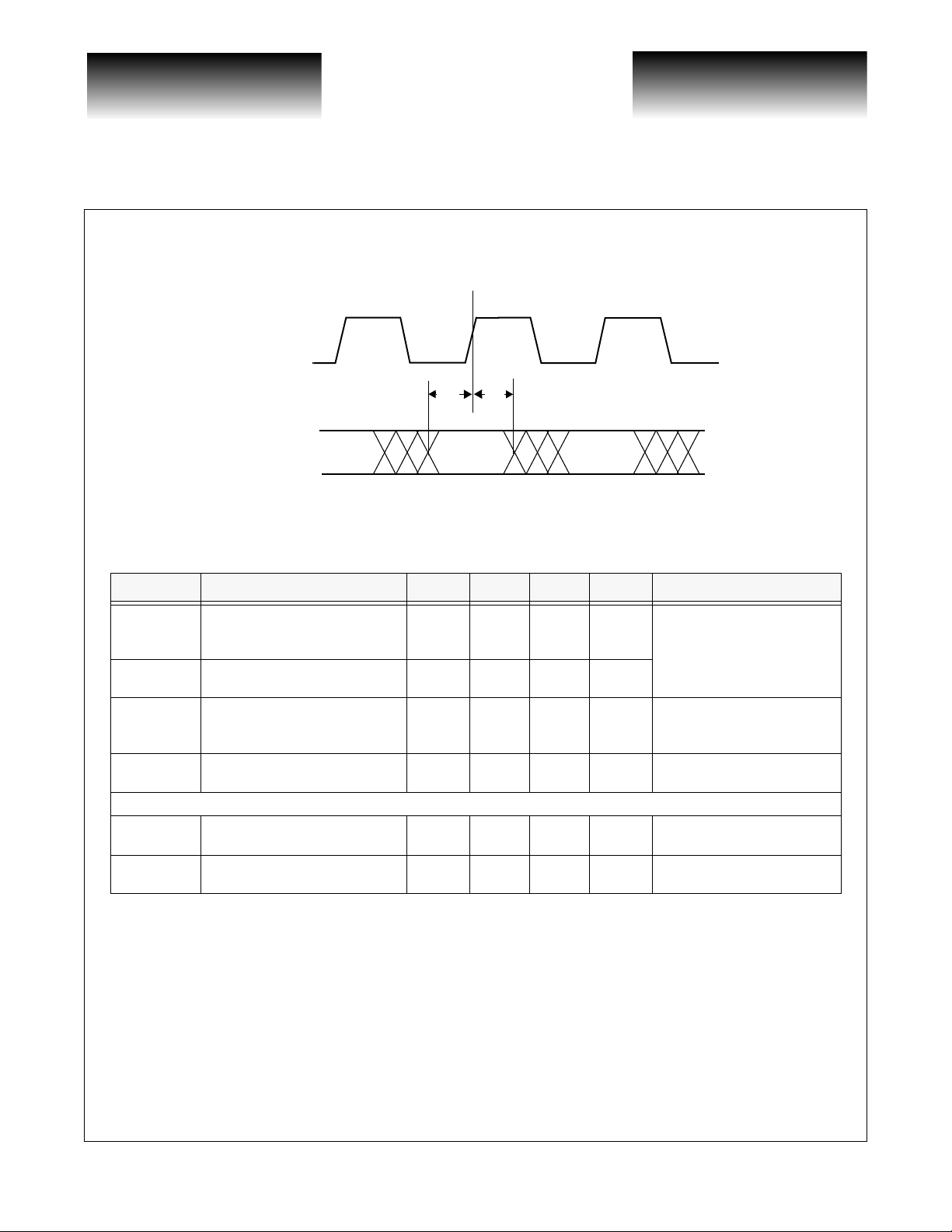
Figure 4: Transmit Timing Waveforms
TBC
T
T
T[0:19]
20-Bit Data
Data Valid
Data Valid
Table 3: Transmit AC Characteristics
Parameters Description Min Typ Max Units Conditions
T
1
T
2
T
SDR,TSDF
T
LA T
T[0:19] setup time to the rising
edge of TBC
T[0:19] hold time after the rising
edge of TBC
TX+/TX- rise and fall time — 160 ps
Latency from rising edge of TBC
to T0 appearing on TX+ TX-
1.5 —ns
1.0 — ns
24 bc
+1ns
Transmitter Output Jitter Allocation
T
RJ
T
DJ
Serial data output random jitter
(RMS)
Serial data output deterministic
jitter (p-p)
— 5 7.5 ps RMS, tested on a sample basis.
—2530ps
2
1
Data Valid
Measured between the valid
data level of T[0:19] to the
1.4V point of TBC.
20% to 80% into 50Ω load to
VSS.
Tested on a sample basis.
45 bc
+1ns
Bit
Clock
Bit clock periods
(PLL locked)
Peak-to-peak, tested on a
sample basis.
VSC7146
Page 6
741 Calle Plano, Camarillo, CA 93012 • 805/388-3700 • FAX: 805/987-5896 8/28/00
VITESSE SEMICONDUCTOR CORPORATION
G52162-0 Rev. 2.7
 Loading...