

VITESSE VSC7140QJ Datasheet
VITESSE
(
)
SEMICONDUCTOR CORPORATION
Data Sheet
SC7140
Features
• Supports ANSI X3T11 1.0625Gb/s, FC-AL
• Implements 2 Hub Nodes
1.0625 Gb/s Fibre Channel
Dual Repeater / Hub Node
Disk Attach for Resiliency
• Provides Bi-directional Signal Clean-u p.
• Dual Digital Clock Recovery Units
• Dual Digital Signal Detect Units
• Dual Port Bypass Circuits
• 106.25 or 53.125 MHz Reference Clock
• 1.2 W Typical Power Dissipation
• 3.3V Power Supply
• 52-Pin, 10mm PQFP
General Description
The VSC7140 is a dual Fibre Channel repeater which can be used in Hubs, JBODs or any Fibre Channel
Subsystem requiring clean in coming and outgoing signals at a bulk head connector. The digital Clock Recovery
Unit (CRU) recovers incoming data from an external device, amplifies it and attenuates jitter. A digital Signal
Detect Unit (SDU) determines whether the incoming signal contains invalid Fibre Channel data. A 2:1 multiplexer forms a Port Bypass Circuit (PBC) to route either recovered incoming data or SI to SO.
Fibre Channel subsystems requiring signal cleanup at the bulkhead would connect RX1 to the incoming
signal and SO1 to the internal subsystem’s input. RX2 would connect to the output of the subsystem and SO2
would connect to the bul khea d.
For Hub applications, SI woul d connec t to the previous Hub Node and output data to the e xt ernal device on
TX. Incoming data from the external device on RX is recovered and cleaned up and passed to the next Hub
node on SO. If the external device is not functional, SI is passed to SO.
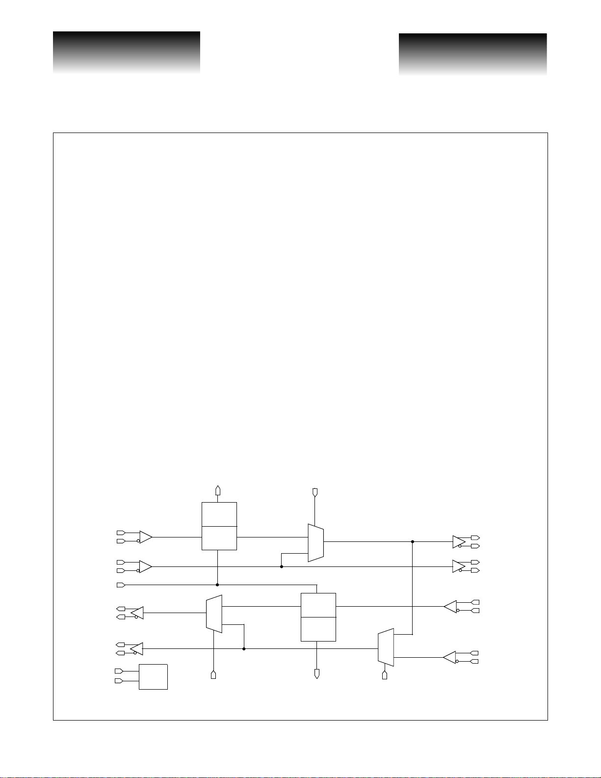
VSC7140 Block Diagram
FAIL1-
SDU1
RX1+
RX1-
SI1+
SI1-
ERRSEL
SO2+
SO2-
TX2+
TX2-
REFSEL
REFCLK
106/53 MHz
G52180-0, Rev 4.0 Page 1
10/23/00
CMU
©
VITESSE SEMICONDUCTOR CORPORATION
CRU1
1
PBC2
0
SEL2
Tel: (800) VITESSE • FAX: (805) 987-5896 • Email: prodinfo@vitesse.com
PBC1
Internet: www.vitesse.com
SEL1
1
0
CRU2
SDU2
1
PBC3
0
FAIL2-
• 741 Calle Plano • Camarillo, CA 93012
HUB
SO1+
SO1-
TX1+
TX1-
RX2+
RX2-
SI2+
SI2-

VITESSE
0
SEMICONDUCTOR CORPORATION
.0625 Gb/s Fibre Channel
Dual Repeater / Hub Node
Data Sheet
VSC714
Functional Description
The VSC7140 contains two fully integrated repeaters to improve signal quality and determine whether the
input to the repeater contains invalid Fibre Channel data. Each repeater consists of a Clock Recovery Unit
(CRU) and a digi tal Si gn al Det ect Un it ( SDU). The CRU locks onto the incoming signal, generates a recov er ed
clock (nominally 1.0625 GHz) and uses this cloc k to resynchr onize the incoming signal. The recovered data
has improved signal qua lity due to amplificatio n and jitter attenuation. Recovered data is retimed to the recovered clock, not to the reference clock, REFCLK. The design of the CRU eliminates the need for any Lock-toReference signal since, in the absence of data, the CRU locks onto REFCLK automatically which eliminates the
need for any external control.
The Signal Detect Units (SDUs) test the recovered data from the CRUs for invalid Fibre Channel data by
looking for run length errors (more than 5 consecutive 1’s or 0’s) and the absence of a seven bit pattern found in
the K28.5 character of either disparity (‘0000101’ or ‘1111010’). This K28.5 pattern should occur between all
valid Fibre Channel frames. The maximum length of a Fibre Channel frame is 2148 bytes (or 21,480 encoded
bits) and the SDU divides time into 1-1/2 maximum frames with a 15-bit counter (~31 microseconds). At the
end of each interval, any run length or K28.5 errors which occured during the interval are stored internally for
use by the state machine which drives the SDU output, FAILn-.
The ERRSEL input controls both SDUs while the FAILn- outputs provide the status of each SDU. ERRSEL selects two different modes generated by the SDU; Single Frame (LOW) or Multiple Frame (HIGH) error
modes. In Single Frame Error Mode, any error condition that occurs within the 1-1/2 frame interval causes
FAILn- to be asserted LO W immedi atel y aft er th at in terval. FAILn- remains asserted until i mmediat ely aft er an
error free interval. In Multiple Fr ame Error Mode, FAILn- is asserted after four consecutive intervals containing
errors and remains asserted until after four consecutive error-free intervals occur. The intent of the Multiple
Frame Error Mode is to allow FAIL1- or FAIL2- to be directly connected to the Port Bypass Circuit controls,
SEL1 or SEL2, in order to configure the part to isolate RX1 or RX2 whenever invalid data is present. Single
Frame Error Mode allows the user to develop their own algorithm for monitoring data and controlling SEL1 or
SEL2.
A TTL reference clock, REFC LK, is use d by the intern al Clock Mu ltiplier Un it (CMU ) to generat e a baud
rate clock (nominally 1.0625 GHz). If REFSEL is HIGH, the CMU multiplies REFCLK (nominally 106.25
MHz) by a factor of 10. If REFSEL is LOW, the CMU multiplies REFCLK (nominally 53.125 MHz) by a factor of 20. The user must ensure that REFSEL is prop erly set in order to match t he frequency of REFCLK.
Three Port Bypass Circuits (PBC) con tain differential 2:1 muxes operating at 1. 0625 Gb/s f or rou ting serial
data. SEL1 configures PBC1 to select either the output of CRU1 (HIGH) or SI1 (LOW) to drive SO1. SEL2
configures PBC2 to select either the output of CRU2 (HIGH) or the output of PBC3 (LOW) to drive SO2.
HUB configures PBC3 to select either the output of PBC1 (HIGH) or SI2 (LOW) to drive the input to PBC2.
©
Page 2 G52180-0, Rev 4.0
VITESSE SEMICONDUCTOR CORPORATION
Tel: (800) VITESSE • FAX: (805) 987-5896 • Email: prodinfo@vitesse.com
Internet: www.vitesse.com
• 741 Calle Plano • Camarillo, CA 93012
10/23/00
VITESSE
SEMICONDUCTOR CORPORATION
Data Sheet
SC7140
1.0625 Gb/s Fibre Channel
Dual Repeater / Hub Node
Application Examples
The VSC7140 is intended for two applications, Dual Repeater or Dual Hub, as configured by HUB. Users
needing to retime both incoming and outgoing signals at the bulkhead of a Fibre Channel system would use the
part in Dual Repeater Mode (HUB is LOW). Users building Fibre Channel Hubs would use the part in Dual
Hub mode (HUB is HIGH) to fully handle the functions of two Hub Nodes.
Dual Repeater Mode
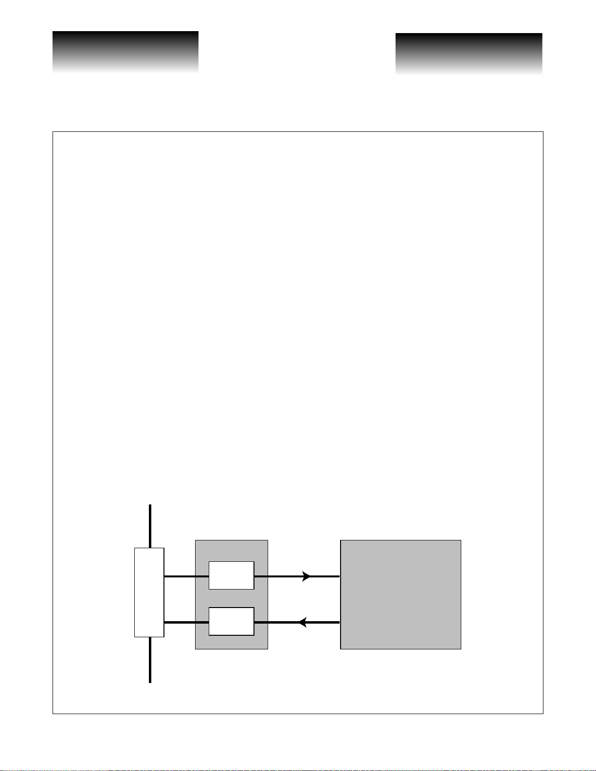
In this example, the VSC7140 forms a dual repeater in a complex Fibre Channel system, such as a JBOD
(Just a Bunch Of Disks) RAID (Redundant Array of Independent Disks) subsystem, which requires the incoming Fibre Channel signal to be retimed to ensure adequate signal quality to the input of the subsy stem. Likewise, the output of the JBOD subsystem requires retiming to ensur e that the outgoing signal from the system
meets the amplitude and jitter requirements of Fibre Channel. For this application, the dual CRUs are the only
circuits required although the SDUs may be used for reporting signal status. Therefore, the VSC7140 would be
configured as follows:
HUB is LOW to select Dual Repeater Mode.
RX1 connects to the external input from the bulkhead.
SO1 connects to the input to the JBOD subsystem.
RX2 connects to the output of the JBOD subsystem.
SO2 connects to the output to the bulkhead.
SI1 and SI2 are not used. Pull up SI1+ and SI2+ to V
TX1 and TX2 are not used. Leave unconnected.
SEL1 and SEL2 are driven HIGH.
FAIL1- and FAIL2- may be used for status. ERRSEL is selected as desired by the user.
with 22k Ohms to prevent input oscillations.
DD
Figure 1: Block Diagram: Use of VSC7140 in Dual Repeater Mode
VSC7140
RX1 SO1
CRU
Internal
Fibre Channel
SO2 RX2
Connector
©
G52180-0, Rev 4.0 Page 3
10/23/00
VITESSE SEMICONDUCTOR CORPORATION
Tel: (800) VITESSE • FAX: (805) 987-5896 • Email: prodinfo@vitesse.com
CRU
• 741 Calle Plano • Camarillo, CA 93012
Internet: www.vitesse.com
Subsystem
VITESSE
0
SEMICONDUCTOR CORPORATION
.0625 Gb/s Fibre Channel
Dual Repeater / Hub Node
Data Sheet
VSC714
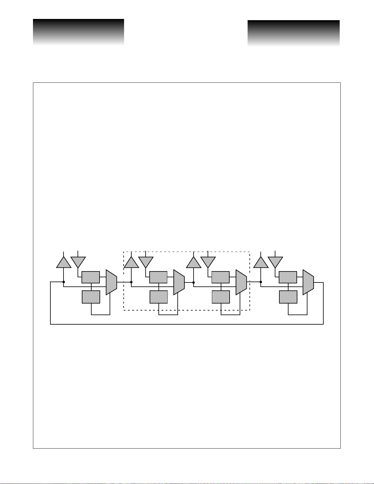
Dual Hub Mode
In this example, the VSC7140 is used to fully implement two adjac ent nodes in a Fibre Ch annel Hub.
Incoming external signals on RX require retiming to improve amplitude and eliminate jitter before being used
by the Hub. The TX outputs drive the external device. A serial loop is formed by daisy chaining the SI to SO
paths of each node. The SDUs are required to configure the Hub to include external devices on the SI/SO loop
if they produce valid Fibre Channel data or to exclude them from the loop if they are not operational.
HUB is HIGH to select Hub Mode.
RX1 connects to the external output from Device #1. TX1 connects to the external input to Device #1.
RX2 connects to the external output from Device #2. TX2 connects to the external input to Device #2.
SI1 is connected to the SO2 output of the previous VSC7140. SI2 is pulled up SI2+ with 22k Ohms.
SO2 is connected to the SI1 input of the next VSC7140. SO1 is left unconnected.
If ERRSEL is HIGH, FAIL1- connects to SEL1 and FAIL2- connects to SEL2.
If ERRSEL is LOW, FAIL1- and FAIL2- are used by off-chip circuits to control SEL1 and SEL2.
Figure 2: Block Diagram: Use of VSC7140 in Hub Mode
CRU
SDU
Note: SO1 and SI2 not used.
TX1 RX2TX2
RX1
VSC7140
SI1
FAIL1
CRU
SDU
SEL1
Internal Loop
FAIL2
CRU
SDU
SO2
SEL2
CRU
SDU
©
Page 4 G52180-0, Rev 4.0
VITESSE SEMICONDUCTOR CORPORATION
Tel: (800) VITESSE • FAX: (805) 987-5896 • Email: prodinfo@vitesse.com
Internet: www.vitesse.com
• 741 Calle Plano • Camarillo, CA 93012
10/23/00
 Loading...