

VITESSE VSC7132YB Datasheet
®
VSC7132
VITESSE
SEMICONDUCTOR CORPORATION
Preliminary Data Sheet
Link Replicator for Fibre
Channel, Gigabit Ethernet and HDTV
Features
• Replicates Fibre Channel, Gigabit Ethernet and
HDTV Links
• T11 Fibre Channel Compliant at 1.0625Gb/s
• IEEE802.3z Gigabit Ethernet Compliant at 1.25Gb/s
• SMPTE-292M Compliant at 1.485Gb/s
General Description
The VSC7132 is a high performance serial Link Replicator for applications in Fibre Channel (1.0625Gb/s),
Gigabit Ethernet (1.25Gb/s) and HDTV (1.485Gb/s). A serializer/deserializer, such as the VSC7123, would
normally be connected to the IN+/- and OUT+/- ports in order to provide duplicate links on the IN0/OUT0 and
IN1/OUT1 ports. A popular application is for Line Cards using serial links from a SerDes (VSC7123) or Serial
Backplane IC (VSC7211) where the VSC7132 provides redundant, hot-swappable links to redundant Switch
Fabric Cards. Another common application is in Host Adapters which require an internal and an external connector where the VSC7132 steers serial data between the SerDes (VSC7123) and the two connectors.
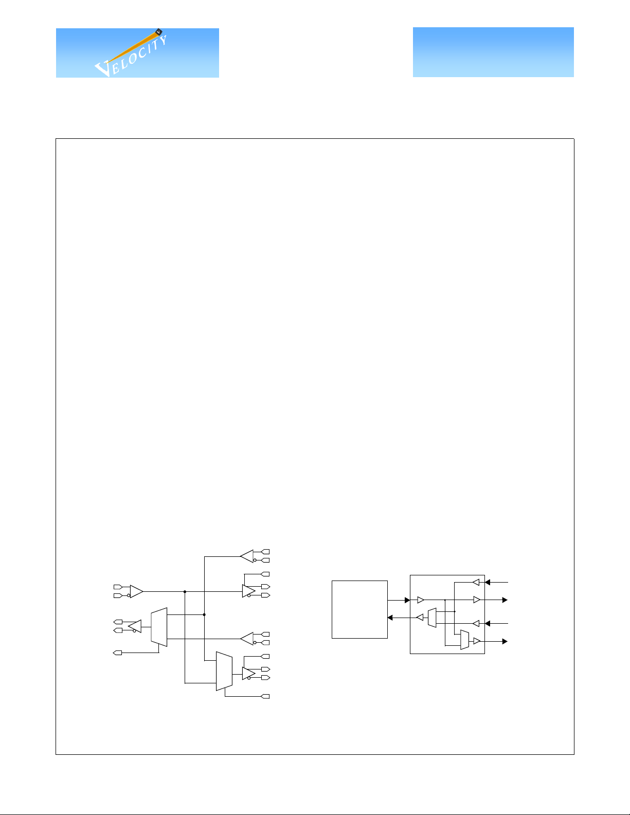
IN is sent to both OUT0 and OUT1 whose buffers are enabled when OE0 and OE1 are HIGH. OUT1 can
select between IN and IN0. OUT can select between IN0 and IN1.
In Link Replicator applications, such as the Line Card to Switch Card links, IN is transmitted to both OUT0
and OUT1, which either IN0 or IN1 is selected at OUT. In Host Adaptor applications, IN goes to OUT0 (an
internal connector) which returns data on IN0. IN0 is looped to OUT1 (an external connector) which returns
data on IN1 and then back to the SerDes on OUT.
• No External Components Required
• 0.4W Maximum Power Dissipation
• 3.3V Power Supply
• 28-Pin, 4.4 x 9.7mm TSSOP Package
G52243-0, Rev 3.0 Page 1
9/21/00
VSC7132 Block Diagram
IN+
IN-
OUT+
OUT-
MUX
0
1
0
1
© VITESSE SEMICONDUCTOR CORPORATION • 741 Calle Plano • Camarillo, CA 93012
Tel: (800)-VITESSE • FAX: (805) 987-5896 • Email: prodinfo@vitesse.com
IN0+
IN0-
OE0
OUT0+
OUT0-
SERDES
IN1+
IN1-
OE1
OUT1+
OUT1MUX1
Internet: www.vitesse.com
VSC7123
TX
RX
VSC7132
LOOP0
LOOP1

®
VSC7132
VITESSE
SEMICONDUCTOR CORPORATION
Link Replicator for Fibre
Preliminary Datasheet
Channel, Gigabit Ethernet and HDTV
Figure 1: Timing Waveforms
IN+/IN0+/IN1+/-
OUT+/OUT0+/OUT1+/-
T
1
T
1
Table 1: AC Characteristics (Over recommended operating conditions)
Parameters Description Min Typ Max Units Conditions
F Operating frequency range 1.0 1.5 Gb/s
T
TR, T
T
1
J
Flow-through propagation delay 7.0 ns
Serial data rise and fall time — 300 ps
F
Deterministic jitter added to serial
input
— 30 ps p-p
— 40 ps p-p
T
J
Delay from any input to any
output.
20% to 80%, tested on a
sample basis
1.0 - 1.25 Gb/s. Measured on
K28.5+, K28.5- pattern
1.25 - 1.5 Gb/s. Measured on
K28.5+, K28.5- pattern
Table 2: DC Characteristics (Over recommended operating conditions)
Parameters Description Min Typ Max Units Conditions
V
IH(TTL)
V
IL(TTL)
I
IH(TTL)
I
IL(TTL)
V
DD
I
DD
P
D
(1)
DV
IN
DV
OUT50
DV
OUT75
NOTE: (1) Refer to Application Note, AN-37, for differential measurement techniques.
Page 2 G52243-0, Rev 3.0
Input HIGH voltage 2.0 — 5.5 V
Input LOW voltage 0 — 0.8 V
Input HIGH current — — 100 mA VIN = 2.4 V
Input LOW current — — –100 mA VIN = 0.5 V
Supply voltage 3.14 — 3.47 V VDD = 3.30V + 5%
Supply current — — 150 mA
Power dissipation 275 400 mW
Receiver differential peak-to-peak
Input Sensitivity, IN, IN0, IN1
Output differential peak-to-peak
(1)
voltage swing, OUT, OUT0, OUT1
Output differential peak-to-peak
(1)
voltage swing, OUT, OUT0, OUT1
© VITESSE SEMICONDUCTOR CORPORATION • 741 Calle Plano • Camarillo, CA 93012
Tel: (800)-VITESSE • FAX: (805) 987-5896 • Email: prodinfo@vitesse.com
300 2600 mVp-p
1000 — 2200 mVp-p 50Ω to VDD – 2.0 V
1200 2200 mVp-p 75Ω to VDD – 2.0 V
Internet: www.vitesse.com
Outputs open, VDD = VDD
max
Outputs open, VDD = VDD
max
AC-Coupled.
Internally biased at VDD/2
9/21/00
®
VSC7132
VITESSE
SEMICONDUCTOR CORPORATION
Preliminary Data Sheet
Link Replicator for Fibre
Channel, Gigabit Ethernet and HDTV
Absolute Maximum Ratings
TTL Power Supply Voltage (VDD) .....................................................................................................0.5V to +4V
PECL DC Input Voltage (V
TTL DC Input Voltage (V
).............................................................................................................–0.5V to VDD +0.5V
INP
) .........................................................................................................................–0.5V to +5.5V
INT
DC Voltage Applied to Outputs for High Output State (V
PECL Output Current, (I
) (DC, Output High)..................................................................................................... –50mA
OUT
Case Temperature Under Bias (TC) .............................................................................................................–55oC to +125oC
Storage Temperature (T
)..........................................................................................................................–65oC to +150oC
STG
Recommended Operating Conditions
Power Supply Voltage (VDD).....................................................................................................+3.14V to +3.47V
Ambient Operating Temperature Range (T) ....................................................................................0oC to +70oC
NOTES: (1) CAUTION: Stresses listed under “Absolute Maximum Ratings” may be applied to devices one at a time without caus-
ing permanent damage. Functionality at or above the values listed is not implied. Exposure to these values for extended
periods may affect device reliability.
(2) Vitesse guarantees the functional and parametric operation of the part under“Recommended Operating Conditions”
except where specifically noted in the AC and DC Parametric Tables
(1)
)...............................................–0.5V to VDD + 0.5V
IN TTL
(2)
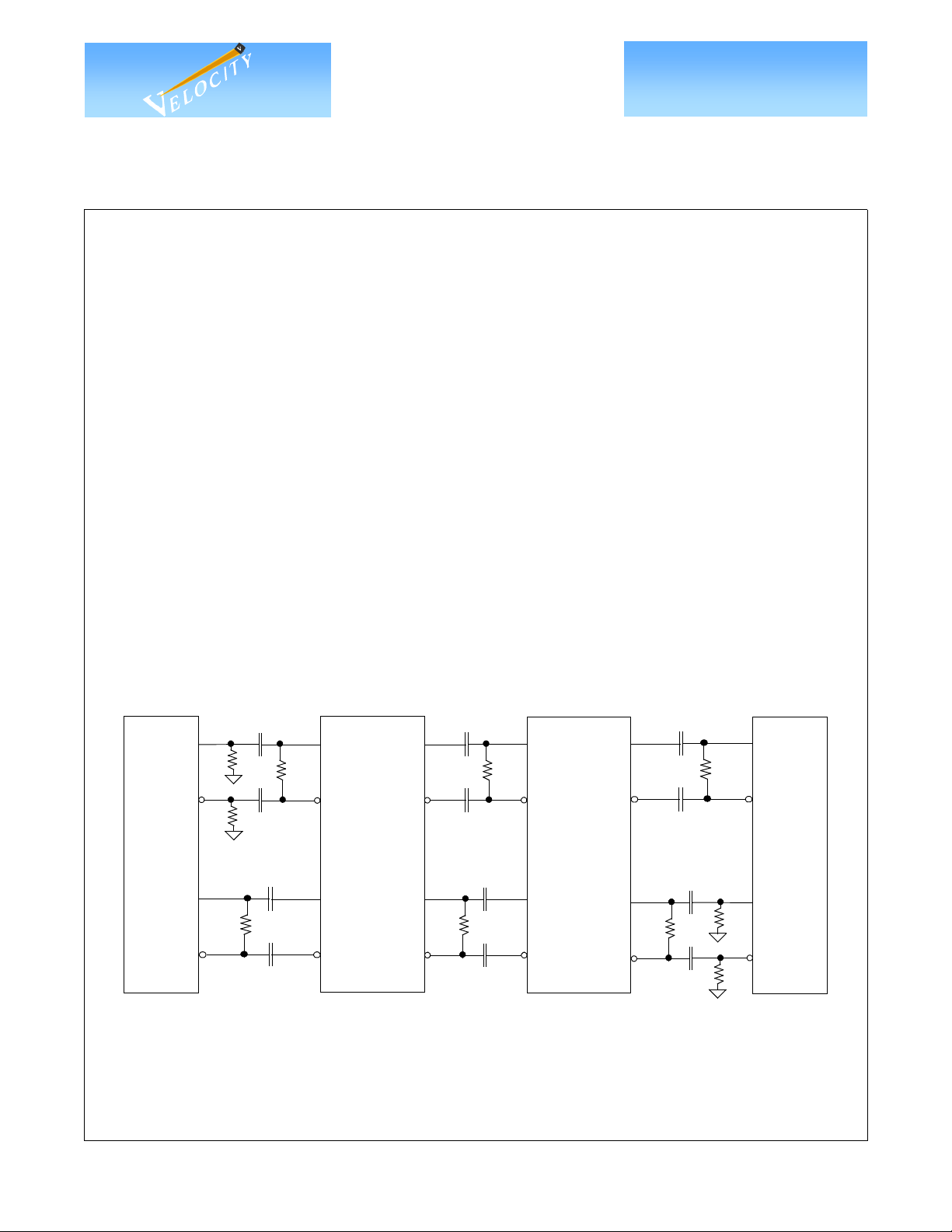
Figure 2: Application Example: VSC7123 and VSC7132 Interconnect
TX+
TX-
VSC7123
RX+
RX-
“R” is 180Ω for 100Ω differential traces or 267Ω for 150Ω differential traces.
“RT” matches the differential impedance of the link.
.01
R
.01
R
.01
RT
.01
I+
RT
I-
VSC7132
O+
O-
O1+
O1-
I1+
I1-
.01
RT
.01
.01
RT
.01
I1+
I1-
VSC7132
O1+
O1-
O+
O-
.01
.01
I+
RT
I-
.01
.01
RX+
RT
RX-
VSC7123
TX+
R
TX-
R
G52243-0, Rev 3.0 Page 3
9/21/00
© VITESSE SEMICONDUCTOR CORPORATION • 741 Calle Plano • Camarillo, CA 93012
Tel: (800)-VITESSE • FAX: (805) 987-5896 • Email: prodinfo@vitesse.com
Internet: www.vitesse.com
 Loading...