

Data Sheet
VSC7130
Dual Repeater/Retimer
for Fibre Channel and Gigabit Ethernet
G52297-0, Rev 4.0 Page 1
04/02/01
© VITESSE SEMICONDUCTOR CORPORATION • 741 Calle Plano • Camarillo, CA 93012
Tel: (800) VITESSE • FAX: (805) 987-5896 • Email: prodinfo@vitesse.com
Internet: www.vitesse.com
VITESSE
SEMICONDUCTOR CORPORATION
Features
General Description
The VSC7130 is used in Fibre Channel (1.0625Gb/s) and Gigabit Ethernet (1 .25Gb/s) systems to provide
bidirectional Clock and Data Recovery (CDR) to ensure standards compliance at critical systems interfaces. As
protocol ASICs integrate multiple SerDes functions, the ASICs tend to be located far from interface connectors
which results in signal degradation and dif fi culty in meet ing indust ry-sta ndard signal quality specificati ons. The
VSC7130 provides a low-cost, easy-to-use solution to this problem by ensuring standards-compliant signal
quality at system interfaces. Additional circuitry implements an FC-AL Hub node.
The VSC7130 provides a pair of bidirect ional CDRs which ca n be conf igured a s either repeat ers or r etimers
or bypassed altogether. Internal system data is recovered and retransmitted with standards-compliant signal
quality at the connector. External receive data from the connector is recovered and retransmitted to the internal
system with increased amplitude and attenuated jitter. An optional Two-Wire Interface allows robust configuration control and status monitoring of the device in order to enhance operation.
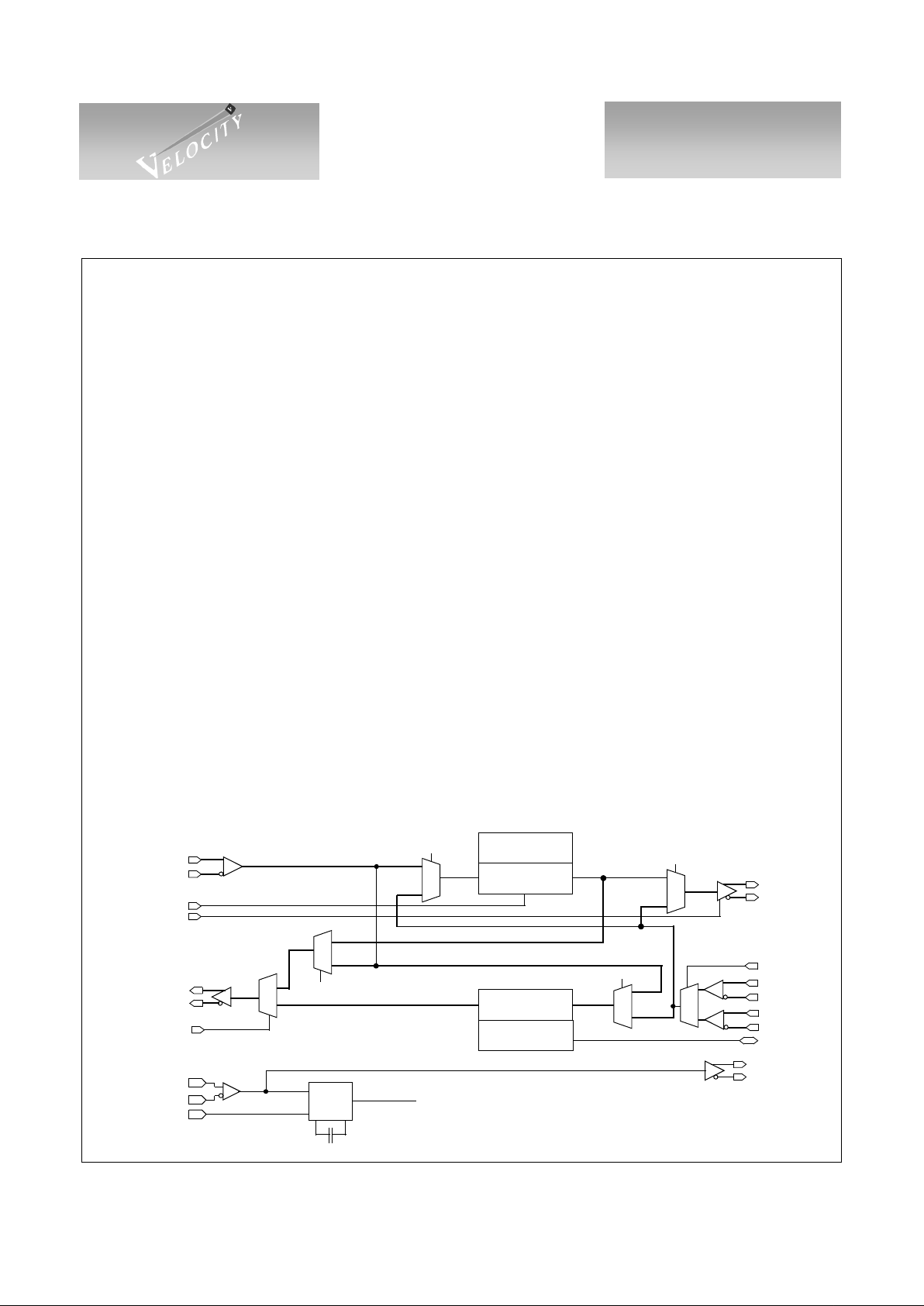
VSC7130 Block Diagram
• Used in Switches, Hubs, GBICs, MIAs and JBODs
• ANSI T11 Fibre Channel Compliant at 1.0625Gb/s
• IEEE 802.3z Gigabit Ethernet Compliant at 1.25Gb/s
• Dual Clock and Data Recovery Units Configurabl e as
Repeaters or Retimers
• Two-Wire Serial Communications Port for Control
and Status
• Combined Analog/Digital Signal Detect Units
• 1/10th or 1/20th Baud Rate TTL/PECL Reference Clock Input and PECL Output
• Bidirectional Analog/Digital Signal Detect
• 3.3V, 850mW Power Typical
• 64-pin, 10x10x1.0mm TQFP Package
• Cost Effective 0.35
µm CMOS Technology
SDET
SI+
SI-
TX+
TX-
SO+
SO-
RX1+
RX1-
CMU
REFI+
REFI-
HALF/FULL
1.0625 GHz
x10/x20
CAP0 CAP1
REFO+
REFO-
NOT SHOWN: Two-Wire Interface, test, modes and RXBIAS
CDR0
CDR1
SDU1
SDU0
MUX1
MUX2
MUX3
TXDIS
RX0+
RX0-
T/R
R1/0
0
1
BYP
1
0
0
1
MUX1SEL
MUX2SEL
0
1
53.125 or106 .25MHz
MUX4
0
1
MUX4SEL
MUX5
1
0
MUX5SEL
Clock Frequencies shown for Fibre Channel
Data Sheet
VSC7130
Dual Repeater/Retimer
for Fibre Channel and Gigabit Ethernet
Page 2 G52297-0, Rev 4.0
04/02/01
© VITESSE SEMICONDUCTOR CORPORATION • 741 Ca ll e Pl an o • Camarillo, CA 93012
Tel: (800) VITESSE • FAX: (805) 987-5896 • Email: prodinfo@vitesse.com
Internet: www.vitesse.com
VITESSE
SEMICONDUCTOR CORPORATION
Applications
Several Fibre Channel and Gigabit Ethernet applications can use the VSC71 30. Configuration changes
between different applications are accomplished with mode pins and the Two-Wire Interface. SI+/- and SO+/-
are normally connected to the duplex i nterface from the sys tem while TX+/- and RX0+/- or RX1+/- are connected to the external link through a connector or optical transceiver. Redundant receive inputs are provided in
order to optimize layouts with copper connectors or optical modules. CDR0 improves the s ignal quality of SI
and retransmits the data on TX. CDR1 improves signal quality of RX0 or RX1 and retransmits recovered data
to SO.
In this document, the term “Repeater” will be used for a clock and data recovery function (CDR) where the
recovered serial data is retransmitted synchronously to the recovered clock. Unlike standard PLL-based CDRs,
this circuit is al l -di gi tal wh ich r esul t s i n good jitter toler anc e, excellent jitter t ransf er a nd low latency in a cir cu it
which performs identically across process, voltage and temperature.
The term “Retimer” is used for a CDR which retransmits the recovered serial data synchronously to the
local reference clock. This complex CDR function eliminates jit te r transfer at th e expe nse of l ate ncy. Due to the
potential mismatch between the baud rate of the incoming data and the local reference clock (i.e. +/-100ppm),
an add/drop elasticity buffer is neede d to insert/delete O rdered Sets to match th is rate difference. The data
which is added/dropped must meet Fibre Channel protocol specifications. By eliminating jitter transfer, standards compliance is ensured. The retimer function is not available for Gigabit Ethernet.
Multi-Node Switch
One application for the VSC7130 is in high port- cou nt Fibre C hanne l and Gigabi t Eth ernet systems such as
switches. Figure 1 shows a switch with a CMOS protocol ASIC with integrated Serializer/Deserializers located
on the Switch Fabric card. Serial data from the protocol ASIC passes through multiple connectors and long
traces on the PCB before reaching the connector. Without the VSC7130, the signal quality at the connectors
would result in poor system performance. However, by using the VSC7130, signal quality is improved to meet
the specifications of Fibre Channel and Gigabit Ethernet at the system interface connectors.
Figure 1: Fibre Channel or Gigabit Ethernet Switch
Protocol ASIC
Switch Fabric Card
Line Card
Connectors
VSC7130
Backplane
Port 1
CDR0>
<CDR1
Port N
Data Sheet
VSC7130
Dual Repeater/Retimer
for Fibre Channel and Gigabit Ethernet
G52297-0, Rev 4.0 Page 3
04/02/01
© VITESSE SEMICONDUCTOR CORPORATION • 741 Calle Plano • Camarillo, CA 93012
Tel: (800) VITESSE • FAX: (805) 987-5896 • Email: prodinfo@vitesse.com
Internet: www.vitesse.com
VITESSE
SEMICONDUCTOR CORPORATION
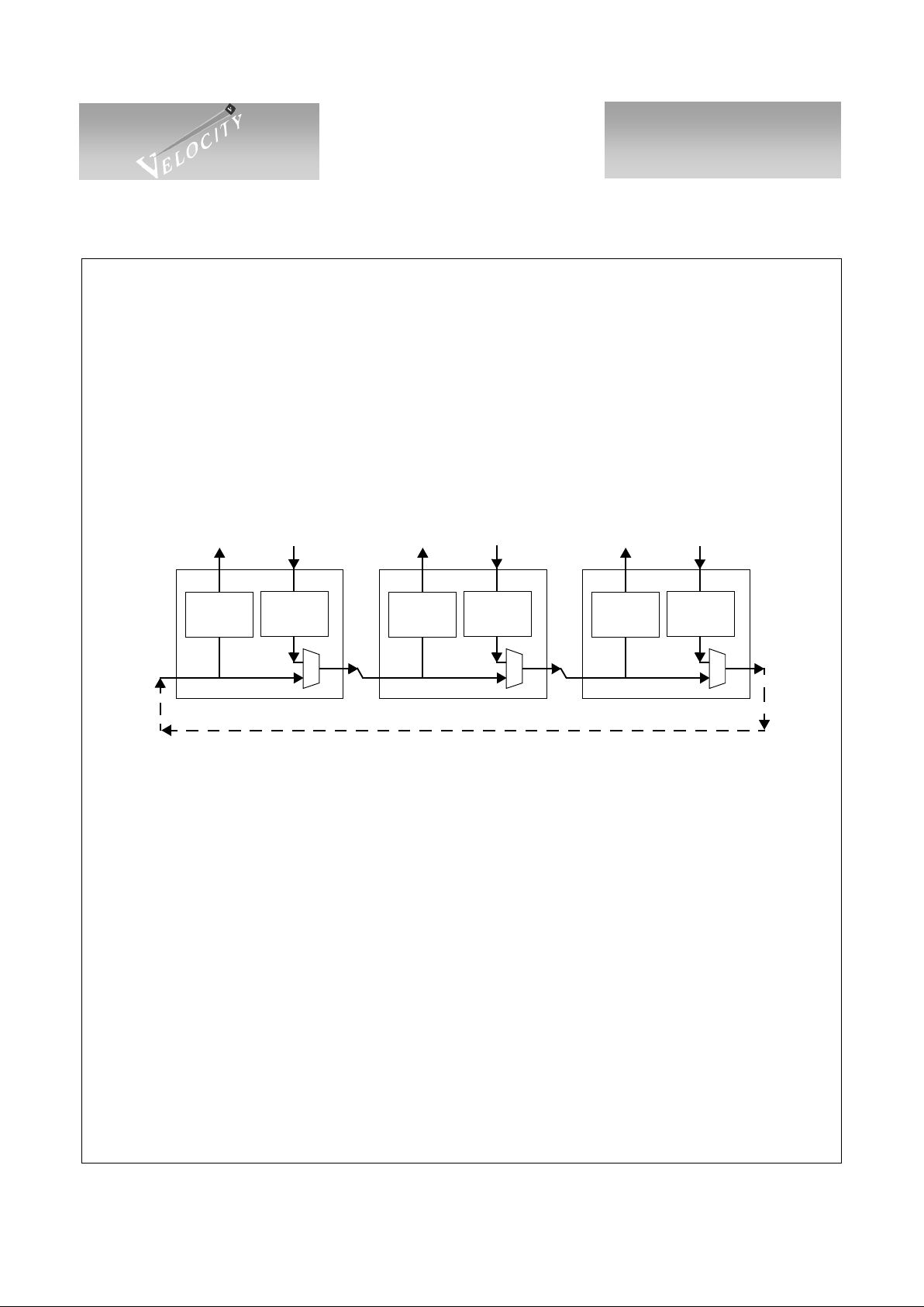
Fibre Channel Hub
The VSC7130 may be used as a single node in a Fibr e Channel A rbitrated Loop Hub. In this application,
incoming data on RX goes through a rep eat er (CDR1) which red uces ji tter. The data is then output on SO to the
next hub node. Incoming data from the previous hub node on SI goes through CDR0 which is configured as a
retimer to eliminate any ji tter ge nera ted inside the Hub . A by pass mu ltip lex er (M UX3) i s us ed t o by pass n odes
which do not have active devi ces connect ed. The si gnal d etection ci rcuitry id entifies v alid dat a at RX in order to
control the configuration of MUX3. The BYP pin may be connected vi a an invert er to SDET, BYP may be con-
trolled externally or MUX3 may be controlled via the Two-Wire Interface.
Access to internal registers through the Two-Wire Interfaces allows numerous features requires by sophi st icated managed Hubs such as Ordered Set Recognition, Ordered Set Generation and simple traffic monitoring.
Figure 2: Fibre Channel Arbitrated Loop Hub
Optical/Electrical Transceiver (GBIC)
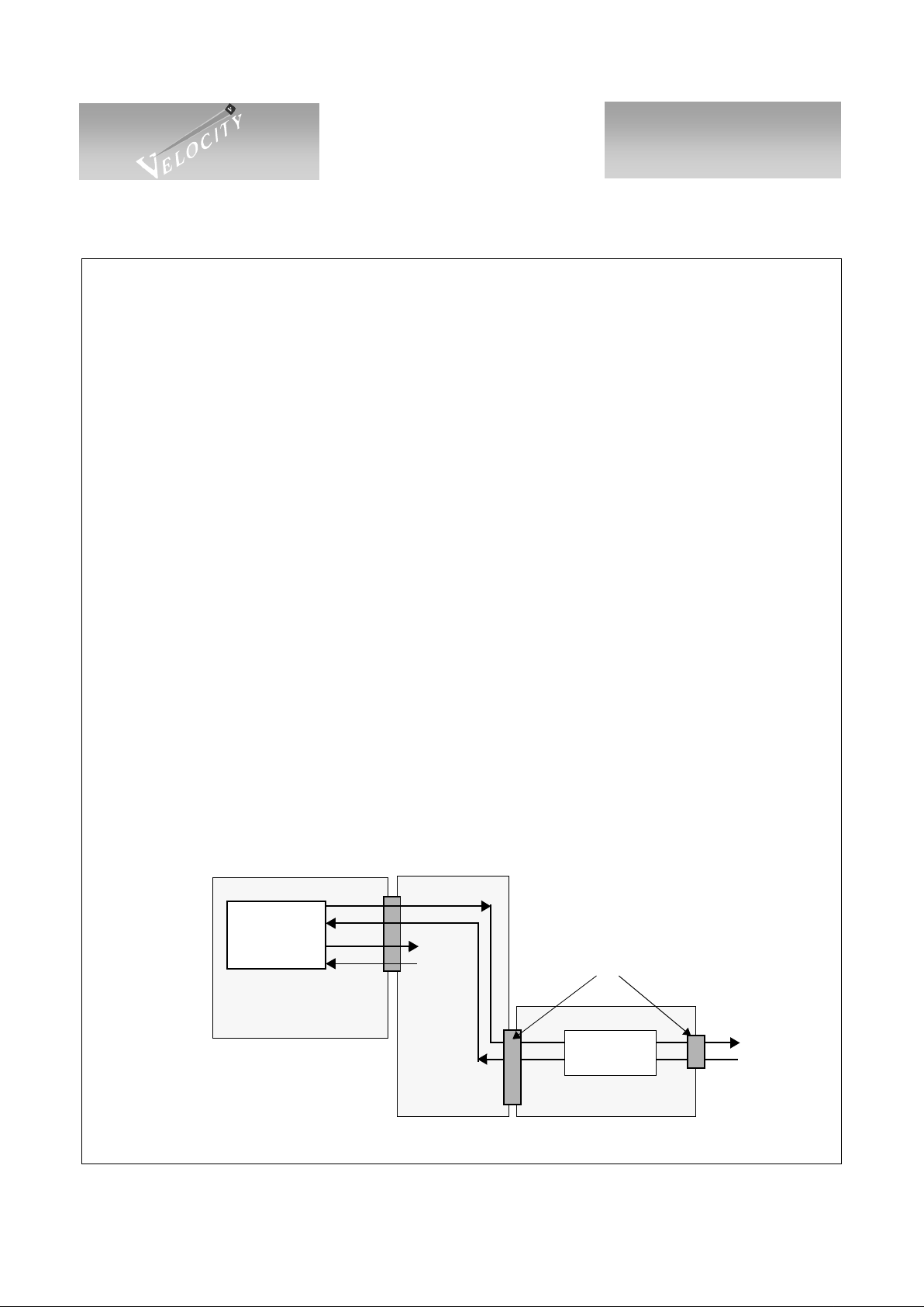
As a dual repeater, the VSC7130 may provi de the func tions requ ired on an Op tical/El ectrical t ranscei ver
such as an Optical or an a active copper Gigabit Interface Converter (GBIC). In this application, outgoing data
from a system goes through CDR0 which can be configured as either a repeater or a retimer. Incoming data
passing through repeater CDR1 is transferred to the system. This function implements the critical circuits in an
active GBIC including RX_LOS.
CDR0
Retimer
CDR1
Repeater
SI
SO
RX
TX
CDR0
Retimer
CDR1
Repeater
SI
SO
RX
TX
CDR0
Retimer
CDR1
Repeater
SI
SO
RX
TX
Internal Loop
External
Device
External
Device
External
Device
Node N-1
Node N+1
MUX3 MUX3MUX3
Node N
Data Sheet
VSC7130
Dual Repeater/Retimer
for Fibre Channel and Gigabit Ethernet
Page 4 G52297-0, Rev 4.0
04/02/01
© VITESSE SEMICONDUCTOR CORPORATION • 741 Ca ll e Pl an o • Camarillo, CA 93012
Tel: (800) VITESSE • FAX: (805) 987-5896 • Email: prodinfo@vitesse.com
Internet: www.vitesse.com
VITESSE
SEMICONDUCTOR CORPORATION
Figure 3: Active Copper GBIC Module
Functionality
Note this datasheet does not co mpletely describe the V SC7130. A c ompanion docume nt, the VSC7130
User’s Manual describes additional applications issues and goes into great depth regarding the Two-Wire Inter-
face and internal register operation.
Notation
All I/O pin names are in bold. All register bit nam es are italicized. Differential signals can be identifi ed
individually, e.g., I0+ and I0-, or together, e.g., I0. Signals and circuits w hich are r epeated a re generica lly
named using an ‘x’ to denote “any channel”, e.g., TXx for any Transmit pins. All registers are identified by
underlining, e.g., CDRxC
and the address for each referenced register will be listed immediately following the
register name (i.e. CDRxC-20h
).
Clock Multiplier Unit and Reference Clock
A reference clock is needed for the c lock multip lier un it (C MU) in o rder to gener ate th e intern al bau d rate
clock. The VSC7130 is used for both Fibre Channel (1.0625Gb /s) and Gigabit Ethernet (1.25Gb/s) appl icatio ns.
The HALF/FUL L signal indicates whether the reference clock is 1/20
th
of the baud rate (HIGH) or 1/10th of
the baud rate (LOW). Table 1 indicates the valid combinations of the HALF/FULL signal and reference clock
frequency. Combinations not listed in the table will result in abnormal functionality.
Table 1: Reference Clock Frequency Selection
HALF / FULL Pin Frequency (MHz) Application
HIGH 53.125 Fibre Channel @ 1.06 25Gb/s
LOW 106.25 Fibre Channel @ 1.0625Gb/s
HIGH 62.5 Gigabit Ethernet @ 1.25Gb/s
LOW 125.0 Gigabit Ethernet @ 1.25 Gb/s
All Other Combinations Not Allowed.
CDR1
Repeater
SO+
SO-
RX+
RX-
CDR0
Repeater
+TX_DAT
-TX_DAT
TX_DISABLE
TX_FAULT
+RX_DAT
-RX_DAT
RX_LOS
MOD_DEF0
MOD_DEF1
MOD_DEF2
SI+
SI-
TX+
TX-
GBIC CONNECTOR, 20-PIN SCA-2
DB-9 or HSSDC
VSC7130
SDET
SERIAL
EEPROM
OSC
TXDIS
RX+
TX+
RX-
TX-
Data Sheet
VSC7130
Dual Repeater/Retimer
for Fibre Channel and Gigabit Ethernet
G52297-0, Rev 4.0 Page 5
04/02/01
© VITESSE SEMICONDUCTOR CORPORATION • 741 Calle Plano • Camarillo, CA 93012
Tel: (800) VITESSE • FAX: (805) 987-5896 • Email: prodinfo@vitesse.com
Internet: www.vitesse.com
VITESSE
SEMICONDUCTOR CORPORATION
Implementing reference clock distribution in multi-node systems can be difficult and expensive if optimal
signal quality is to be achieved. In order to reduce this bur den, the VSC7130 has a flexible reference input
buffer which can be either single- ended TTL, or differential PECL. If si ngl e-ended TTL, REFI+ should be connected to the clock source and REFI- should be left unconnected. REFI- is biased to V
DD
/2 for TTL thresh-
olds. If a PECL source is used, connect the positive side to REFI+ and the negative side to REFI-. In order to
provide the reference clock to multiple devices, a reference clock output, REFO+/-, is provided which is just a
PECL buffered version of REFI+/-. In this way, multiple VSC7130s m ay be daisy chained together with the
REFO driving the REFI of the next device. When REFO is driving REFI, a 100
Ω resistor should be con-
nected between REFI+ and REFI-.
The reference clock is used by the clock multiplier unit (CMU) in order to gener ate the internal baud rate
clock. In order to maximize signal quality of the TX and SO outputs, the REFI input should be of the highest
quality possible with sharp edges and l ow jitt er. Duty cycle distortion is not very important sinc e only the rising
edge of REFI is used. The CMU is a high perfor mance an alog PLL w hich multiplies the reference clock frequency by 20 or 10 depending on HALF/FULL.
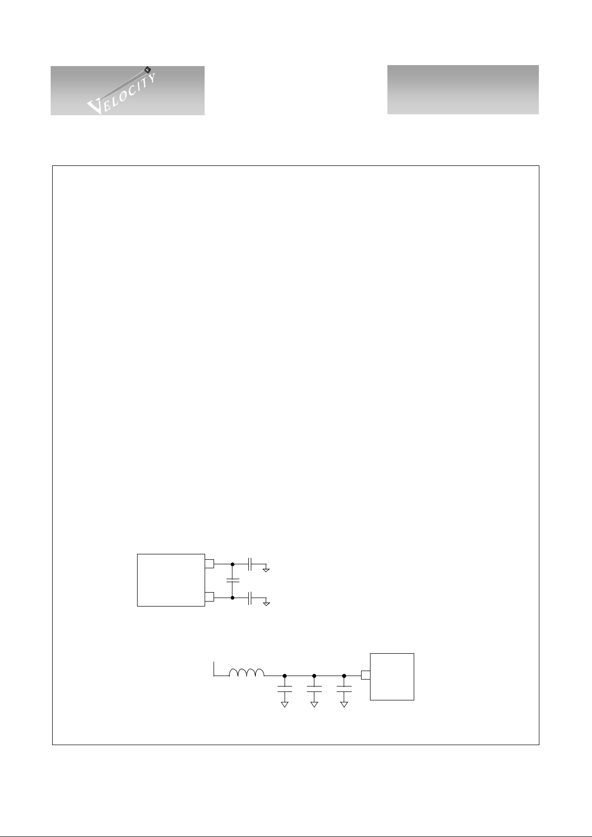
The on-chip PLL uses a single external 0.1µF capacitor, connected between CAP0 and CAP1, to control
the Loop Filter. This capacitor should be a multilayer ceramic dielectric, or better, with at least a 5V working
voltage rating and a good temp erat ure coefficient, i.e. NPO is preferred but X7R is acceptable. The se capacitors
are used to minimize the impact of common mode noise on the CMU , especially power supply noise. Higher
value capacitors provide better robust ness in syste ms. NPO i s preferred becau se i f an X7R capacitor is used, the
power supply noise sensitivity will vary with temperature. For best noise immunity, the designer may use a
three capacitor circuit with one differential capacitor between CAP0 and CAP1, C1, a capacitor from CAP0 to
ground, C2, and a capacitor from CAP1 to ground, C3. Lar g er values are be tter but 0.1µF i s adequat e. However,
if the designer cannot use a three capacitor circuit , a si ngl e differential capacitor, C1, is adequate. These components should be isolated from noisy traces. Figure 4 is the recommended Loop filtering scheme.
Separate power (VDDA) and ground (VSSA) are provided in order to allow a separately filtered power
supply to reduce noise. Figure 5 is the recommended VDDA filtering scheme.
Figure 4: Loop Filter Capacitors (Recommended Circuit)
Figure 5: VDDA Filtering (Recommended Circuit)
CAP0
CAP1
C1
C2
C3
VSC7130
C1=C2=C3= >0.1µF
MultiLayer Ceramic
Surface Mount
NPO (Preferred) or X7R
5V Working Voltage Rating
VDDA
VDD
C1=10-33µF
C3C2C1
L1
C2=0.1µF
C3=0.01µF-0.001µF
L1=Ferrite bead with
high impedance at high frequencies
and some DC resistance (0.5
Ω)
VSSA
VSC7130

Data Sheet
VSC7130
Dual Repeater/Retimer
for Fibre Channel and Gigabit Ethernet
Page 6 G52297-0, Rev 4.0
04/02/01
© VITESSE SEMICONDUCTOR CORPORATION • 741 Ca ll e Pl an o • Camarillo, CA 93012
Tel: (800) VITESSE • FAX: (805) 987-5896 • Email: prodinfo@vitesse.com
Internet: www.vitesse.com
VITESSE
SEMICONDUCTOR CORPORATION
Input and Output Buffers, Analog Signal Detection, Cable Equalization
The RX0+/-, RX1+/- and SI+/- differential i nputs are h igh performa nce inpu t buffers which amplify the
incoming signal. Furthermore, a cable equalization circuit is included in the input buffer which accentuates
high frequency signals in order to co mpensate for the high frequenc y loss found in copper cable s and traces .
This cable equalization circuit enhances the ability of the VSC7130 to reliably receive serial inputs which have
been degraded with jitter. The RX 1+/- input buffer also includes an analog signal detection circuit which has
adjustable thresholds set by the external RXBIAS pin (see Figure 9). The output of this signal is processed further in the Signal Detection circuitry described elsewhere, as well as selectable threshold levels which are
selected with the RXBIAS input.
If the Two-Wire Interface is not used, R1/0 directly controls the RX0 and RX1 input buffers and Cable
Equalization is enab led in SI, RX0 and RX1. If the Two-Wi re Interface is used, microcontroller control allows
enabling or disabling of the cable equalization circuit.
Please refer to the VSC7130 User’s Manual for a more complete description of the input and output buffer
controls and cable equalization controls.
High-Speed I/O Termination Schemes
The high-speed I/O lines for the VSC7130 require the standard Vitesse 1Gb/s CMOS device termination
schemes. Plea se re fe r to the Termination for 1Gb/s CMOS Devices Applicatio n Note (AN-54) fo r VSC7130 RX
and TX termination schemes. When using the REFI+/- and REFO+/- pins on the VSC7130 in daisy-chained
clock applications, specific termination must be implemented. If the REFO+/- pins of one VSC7130 are to be
routed to the REFI+/- pins of a second VSC7130, 50
Ω single-ended (100Ω differential) traces should be used.
AC coupling caps should be placed between the two VSC7130s. Additionally, a 100
Ω 1% termination resistor
should be place between the REFI+ and REFI- lines of the second VSC7130. This termination resistor should
be located as close to the REFI+/- pins as possible. Figure 6 shows the recommended termination and compo-
nents when using the VSC7130’s REFI and REFO.
Figure 6: REFI and REFO Recommended Termination
VSC7130 #1
REFI+
REFI-
REFO+
REFO-
Oscillator
(TTL)
53.125 or 106.25MHz
X
VSC7130 #2
REFI+
REFI-
REFO+
REFO-
22
Ω
100
Ω
1%
0.01µF
0.01
µ
F
50
Ω
1%
50
Ω
1%
0.01µF
0.01µF
Data Sheet
VSC7130
Dual Repeater/Retimer
for Fibre Channel and Gigabit Ethernet
G52297-0, Rev 4.0 Page 7
04/02/01
© VITESSE SEMICONDUCTOR CORPORATION • 741 Calle Plano • Camarillo, CA 93012
Tel: (800) VITESSE • FAX: (805) 987-5896 • Email: prodinfo@vitesse.com
Internet: www.vitesse.com
VITESSE
SEMICONDUCTOR CORPORATION
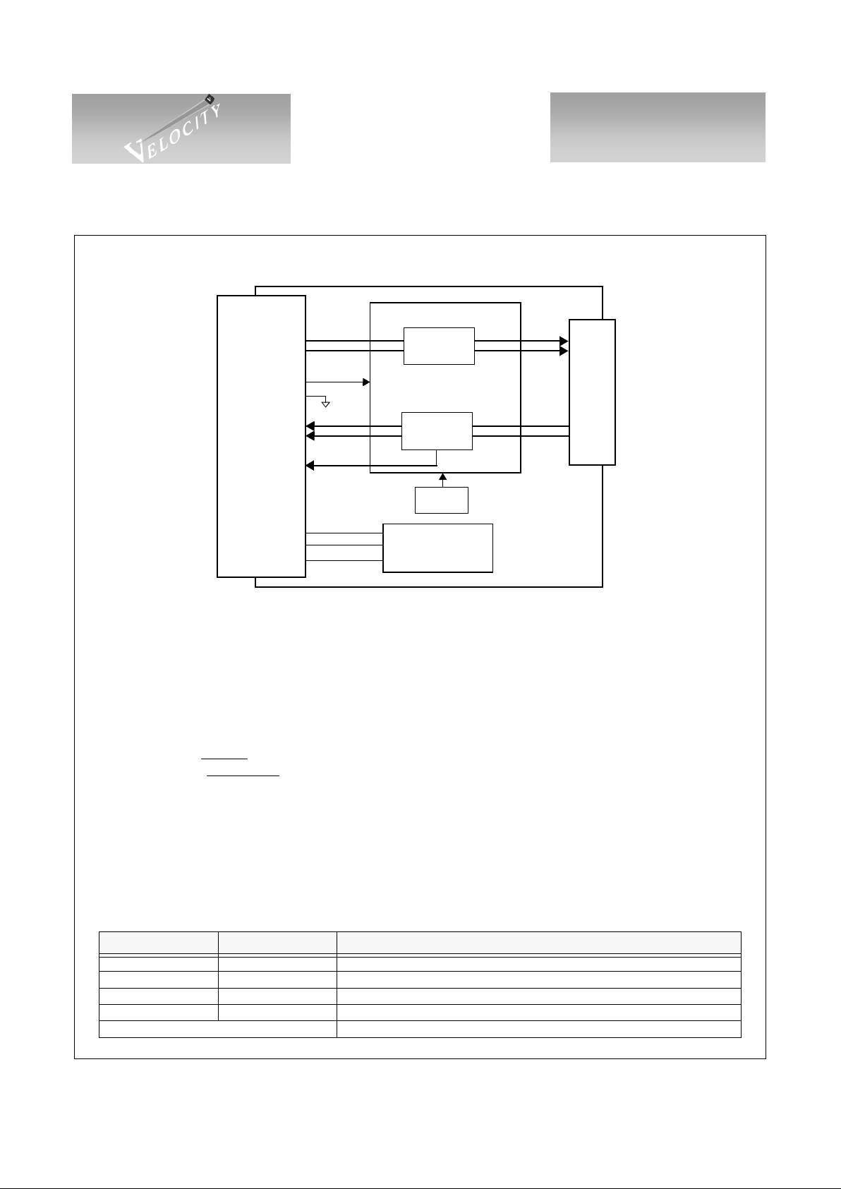
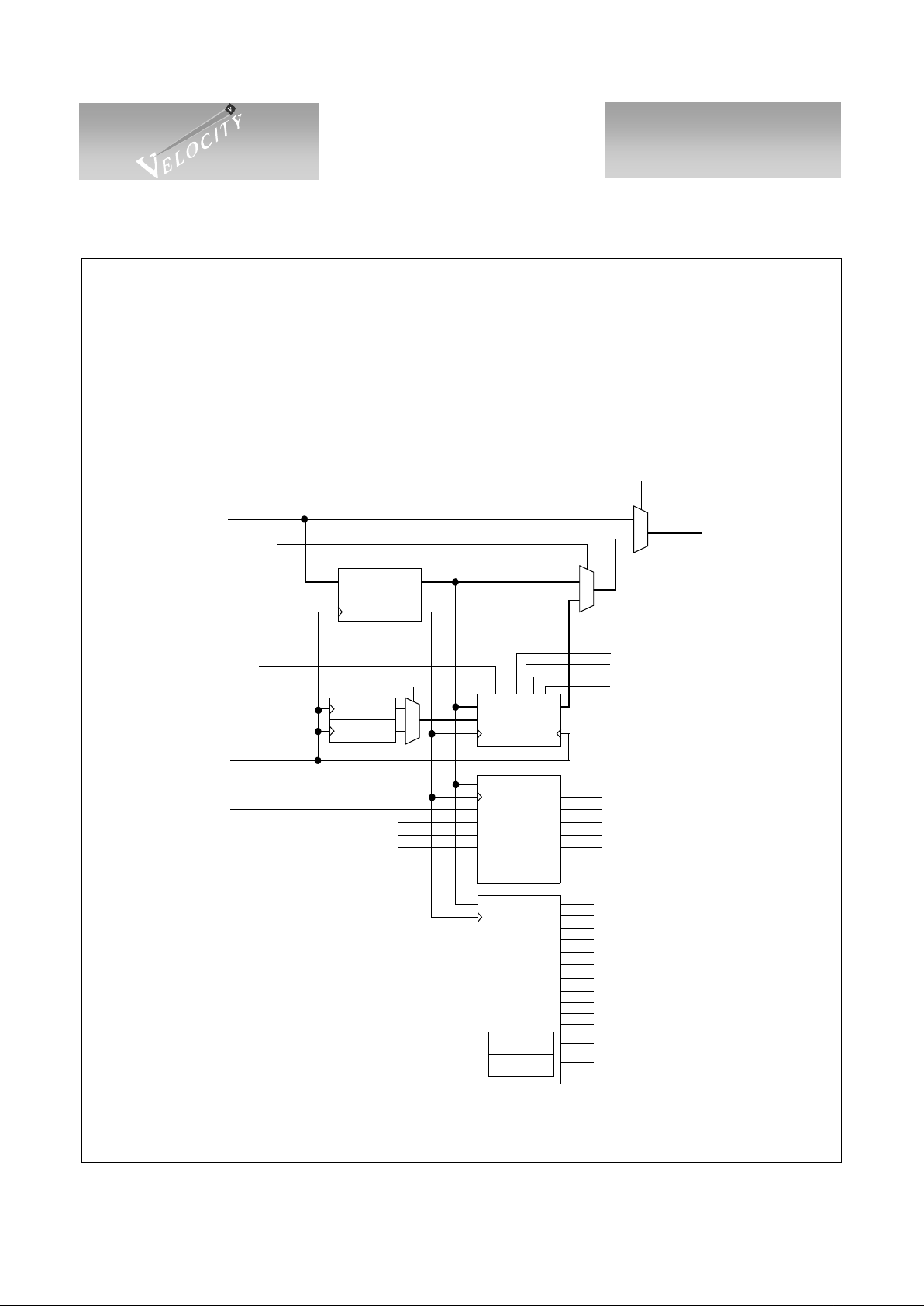
Clock and Data Recovery (CDR)
Two Clock and Data Recovery Units (CDR) are included in the VSC713 0 in order to improve signal qual ity of
serial data by amplification and jitter attenuation. Figure 7 shows a block diagram of each CDR with its corresponding Signal Detect Unit (SDU). Table 2 shows how each CDR may be configured as either a repeater or a
retimer using the MODE0, MODE1 and T/R pins or via the Two-Wire Interface by programming the MODEDIS,
T/RDIS and ITRx register bits.
Figure 7: CDRx/SDUx Block Diagram
OSGxSEL
Q
CLKO
D
REPEATERx
OSGENxA
OSGENxB
0
1
Serial In
Serial Out
RLLDISx
K28DISx
RLLx
K28x
ASDx
ASDDISx
KWINDx(5:0)
PSDx
QD
RETIMERx
D
SDUx
SDx
Analog Signal Detect In
Baud Rate Clock
D
HUB
IDLEx
Support
(from CMU)
BYPx
OSREC0A
OSREC0B
ARBx
OPENx
CLSx
OSRxA
OSRxB
LIPF7,F7x
LIPF8,F7X
LIPF7,Xx
LIPF8,Xx
LIPYXx
ADDx
DROPx
OVERx
(from input buffer)
UNDERx
LIPFFx
NLIPF8x
1
0
1
0
SELRTx
(derived from
MODE[1:0], T/R
,
MODEDIS, T/RDIS and
and ITRx)
OSGENx
 Loading...