

VITESSE VSC7129T-QM, VSC7129R-QM, VSC7127T-QM, VSC7127R-QM Datasheet
Data Sheet
VSC7127/VSC7129
Family of Repeater/Retimer and Port
Bypass Circuits for Fibre Channel
G52298-0, Rev 4.3 Page 1
05/01/01
© VITESSE SEMICONDUCTOR CORPORATION • 741 Calle Plano • Camarillo, CA 93012
Tel: (800) VITESSE • FAX: (805) 987-5896 • Email: prodinfo@vitesse.com
Internet: www.vitesse.com
VITESSE
SEMICONDUCTOR CORPORATION
Features
General Description
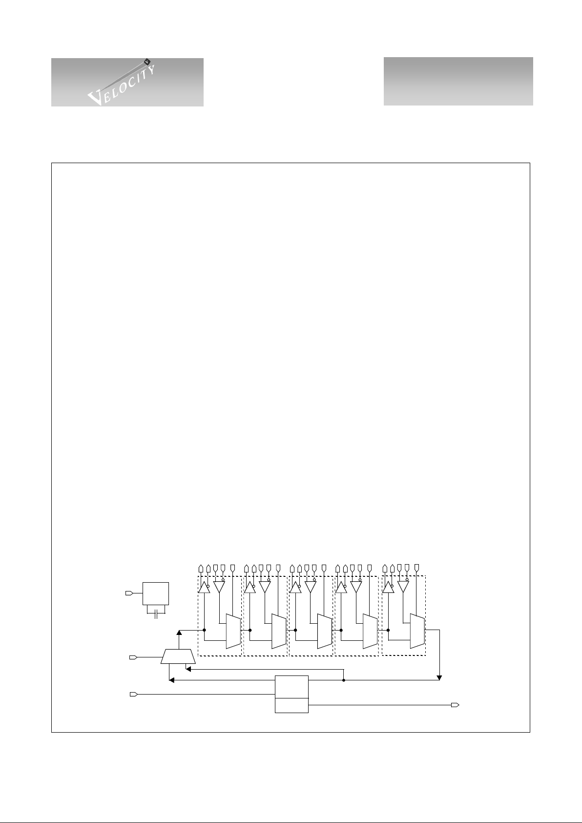
The VSC7127 and VS C7129 contain s ix ca scaded Port By pass C ircuits (PB Cs), th e FibreTimer™ configurable Repeater/Retimer (CRU) and a Signal Detect Unit (SDU). These parts are typically used in distributing
Fibre Channel signals to an array of disk drives in an FC-AL loop as illustrated in Figure 1. The first
VSC7127’s CRU is configured as a Repeater to attenuate jitter, the second VSC7127’s CRU is bypassed to
reduce power and the third VSC7127’s CRU is configured as a retimer so that t he output of the device is a jit ter -
compliance point.
Each PBC is a multiplexer that is controlled by the corresponding SELx line which, if HIGH, selects the
external input or, if LOW, selects the output of the previous PBC. For the VSC712xR, when MODE is LOW
and SEL5 is HIGH, the CRU is a sophisticated repeater which has low latency, no peaking and attenuates jitter
even at low frequencies. When MODE is HIGH and SEL5 is HIGH, the CRU is a retimer which eliminates jitter transfer but has increased latency due to an elasticity buffer which adds/drops Fibre Channel fill words in
order to accomodate the difference between the bau d rate of the incom ing data and t he local REFCLK. Wh en
SEL5 is LOW, the CRU i s bypassed and powered down. The SDU monitors the analog levels of the IO+/- i nput
and monitors the out pu t of the CRU digitally to indicate whether va lid data is present.
The VSC7127/VSC7129 are similar t o th e VSC7124 which does not contain the FibreTimer
™
cell or CMU.
VSC7127/VSC7129 Block Diagram
• ANSI X3T11 Fibre Channel Compliant
• 1.0625Gb/s Operation
• Features the FibreTimer
™
Configurable Clock
Recovery Unit (CRU): Repeater, Retimer or
Bypassed
• Six Port Bypass Circuits (PBC)
• Analog/Digital Signal Detect (SDU)
• On-Chip Transmit Termination
• 3.3V, 700mW Power Dissipation
• Compatible with HDMP-0451 (VSC7127) or
HDMP-0452 (VSC7129)
• 44-Pin, 10mm PQFP Package
I1+
I1-
O1-
SEL1
1
0
PBC1
REFCLK
SDU
CRU
I2+
I2-
O2+
O2-
SEL2
1
0
PBC2
I3+
I3-
O3+
O3-
SEL3
1
0
PBC3
I4+
I4-
O4+
O4-
SEL4
1
0
PBC4
CMU
SIGDET
0.1uF
MODE
O1+
I0+
I0-
O0+
O0-
SEL0
1
0
PBC0
106.25MHz
01
PBC5
SEL5

Data Sheet
VSC7127/VSC7129
Family of Repeater/Retimer and Port
Bypass Circuits for Fibre Channel
VITESSE
SEMICONDUCTOR CORPORATION
Page 2 G52298-0, Rev 4.3
05/01/01
© VITESSE SEMICONDUCTOR CORPORATION • 741 Calle Plano • Camarillo, CA 93012
Tel: (800) VITESSE • FAX: (805) 987-5896 • Email: prodinfo@vitesse.com
Internet: www.vitesse.com
Application: Fibre Channel Disk Arrays
A 12-port JBOD is shown in Figure 1. Thi s dual loop application use s 3 VSC 712 7Xs on e ach l oop in or der
to configure the FC-AL disk arra y. Functional drives are included in the FC-AL loo p while non- functional or
missing drives (numbers 2, 7, 9) are excluded.
Figure 1: 12-Drive FC-AL JBOD Application
VSC7127R #1
VSC7127R #2
VSC7127 R#3
VSC7127R #4
7125
VSC7121 QUAD PORT BYPASS CIRCUIT
Optics
or
Copper
SerDes
7125
SerDes
1
0
1
0
10
1
0
7125
SerDes
7125
SerDes
10
1
0
7125
SerDes
7125
SerDes
1
0
10
7125
SerDes
7125
SerDes
10
10
7125
SerDes
7125
SerDes
1
0
10
1
0
1
0
7125
SerDes
7125
SerDes
1
0
1
0
1
0
1
0
7125
SerDes
7125
SerDes
10
1
0
7125
SerDes
7125
SerDes
10
1
0
7125
SerDes
7125
SerDes
10
10
Repeater
Retimer
Retimer
Repeater
VSC7127T #5
1
2
3
4
5
6
7
8
9
10
11
12
VSC7127T #6
Optics
or
Copper
LOOP A
LOOP B
CONFIGURATION:
7127R #1 & 2: Repeater Mode
SEL0=1, SEL5=1
7127T #5 & 6: Retimer Mode
SEL1=1, SEL5=1
MODE=0
MODE=1
7127R #3 & 4: By pass Mode
SEL5=0
MODE=x, No REFCLK
0
1
2
3
4
0
0
1
2
3
4
0
1
1
2
3
4
0

Data Sheet
VSC7127/VSC7129
Family of Repeater/Retimer and Port
Bypass Circuits for Fibre Channel
G52298-0, Rev 4.3 Page 3
05/01/01
© VITESSE SEMICONDUCTOR CORPORATION • 741 Calle Plano • Camarillo, CA 93012
Tel: (800) VITESSE • FAX: (805) 987-5896 • Email: prodinfo@vitesse.com
Internet: www.vitesse.com
VITESSE
SEMICONDUCTOR CORPORATION
Functionality
Device Configurations
Four devices are specified in this da tasheet: VSC7127R , VSC7127T, VSC7129R and VSC7129T. The
VSC7127 is pin-compatible to the HDMP-0451. The VSC7129 is pin com patible with the HDM P-0452. The
VSC712xR is configured as a Repeater when pin 12, MO DE, is LOW, or a Retimer when HIGH. The
VSC712xT is configured as a Retimer when pin 12, MODE, is LOW, or a Repeater when HIGH.
Port Bypass Circuits
The VSC712x contains six Port Bypass Circuits (PBCs) which are 2-to-1 multiplexers used to steer serial
signals. Each PBC, PBCx has a single select line, SELx, which when HIGH, selects the external input, Ix, to
PBCx and when LOW, selects the outp ut of the previous PBC. PC B5 does not ha ve an ext ernal i nput but select s
between the output of the CRU (when SEL5 is HIGH) and the output of PBC0 (when SEL5 is LOW). These
controls allow FC-AL loops to include a functional device on the loop or exclude a non-functional device from
the loop.
FibreTimer™ Clock Recovery Unit—Repeater Mode
The Clock Recovery Unit (CRU) is a digital PLL which extracts the clock from the incoming data and samples the data with the extracted clock. In repeater mode, the output of the CRU is synchronized to the recovered
clock and has improved signal quality due to amplification of th e signal and attenu ation of jitter. Latency
through the device is quite low, just a few bit times. Multiple repeaters can be cascaded without accumulation
of jitter. MODE determines whether the CRU is a Repeater o r a R etimer.
FibreTimer™ Clock Recovery Unit —Retimer Mode
MODE may configure the CRU as a retimer where the recovered data is placed into an elasticity buffer.
Data is taken out of the elasticity buffer and retransmitted synchronously to the local REFCLK. For Fibre Channel data, Fill words will be added and dropped in the elasticity buffer in order to accomodate the differences in
speed between the incoming data and the REF CLK. The retimer does not transfer jitter from the input to the
output but has longer latency, up to 4 word times, through the device.
FibreTimer™ Clock Recovery Unit—Bypass Mode
When SEL5 is LOW, PBC5 selects the output of PBC0 and the CRU is unused . In this mode, the CRU is
powered down to reduce power dissipation. If the part will be used only in this mode, REFCLK and MODE are
ignored and can be left open. If the CRU is bypassed, the Signal Detect Unit is disabled and the output is LOW.
Signal Detection
A signal detect unit (SDU) monitors IO+/- and the output of the CRU to determine if there is a valid Fibre
Channel signal present. The SI GDET is update d every 1 60 b its (an “interval”) with the previous interval’s status
of three different Signal Detect Units: analog signal amplitude (ASDU), run length check (RLLSDU), Ordered
Set density (OSSDU). If the input amplitude is less than 200mV (differential), ASDU will be set LOW. If the
input amplitude is greater than 400mV, ASDU will be asserted HIGH. If a run length vi olation occurs (more
than 5 consecutive ones or zeros), the RLLSDU will be set LOW and stay LOW until the occurrence of a valid
Data Sheet
VSC7127/VSC7129
Family of Repeater/Retimer and Port
Bypass Circuits for Fibre Channel
VITESSE
SEMICONDUCTOR CORPORATION
Page 4 G52298-0, Rev 4.3
05/01/01
© VITESSE SEMICONDUCTOR CORPORATION • 741 Calle Plano • Camarillo, CA 93012
Tel: (800) VITESSE • FAX: (805) 987-5896 • Email: prodinfo@vitesse.com
Internet: www.vitesse.com
Fill Word or Primitive Sequence. Any Fill Word or Primitive Sequence will reset the OSSDU counter which
will increment on any 160-bit sequence which is not a Fill Word or Primitive Sequence. If the counter reaches
256, a Fill Word or Primitive Sequence has not occured often enough so OSSDU is asserted until reset again.
SIGDET is just an or’ing of these three state machines resynchronized to the 160-bit interval clock.
If SEL5 is LOW or REFCLK is absent, the signal detect unit is disabled and SIGDET is LOW.
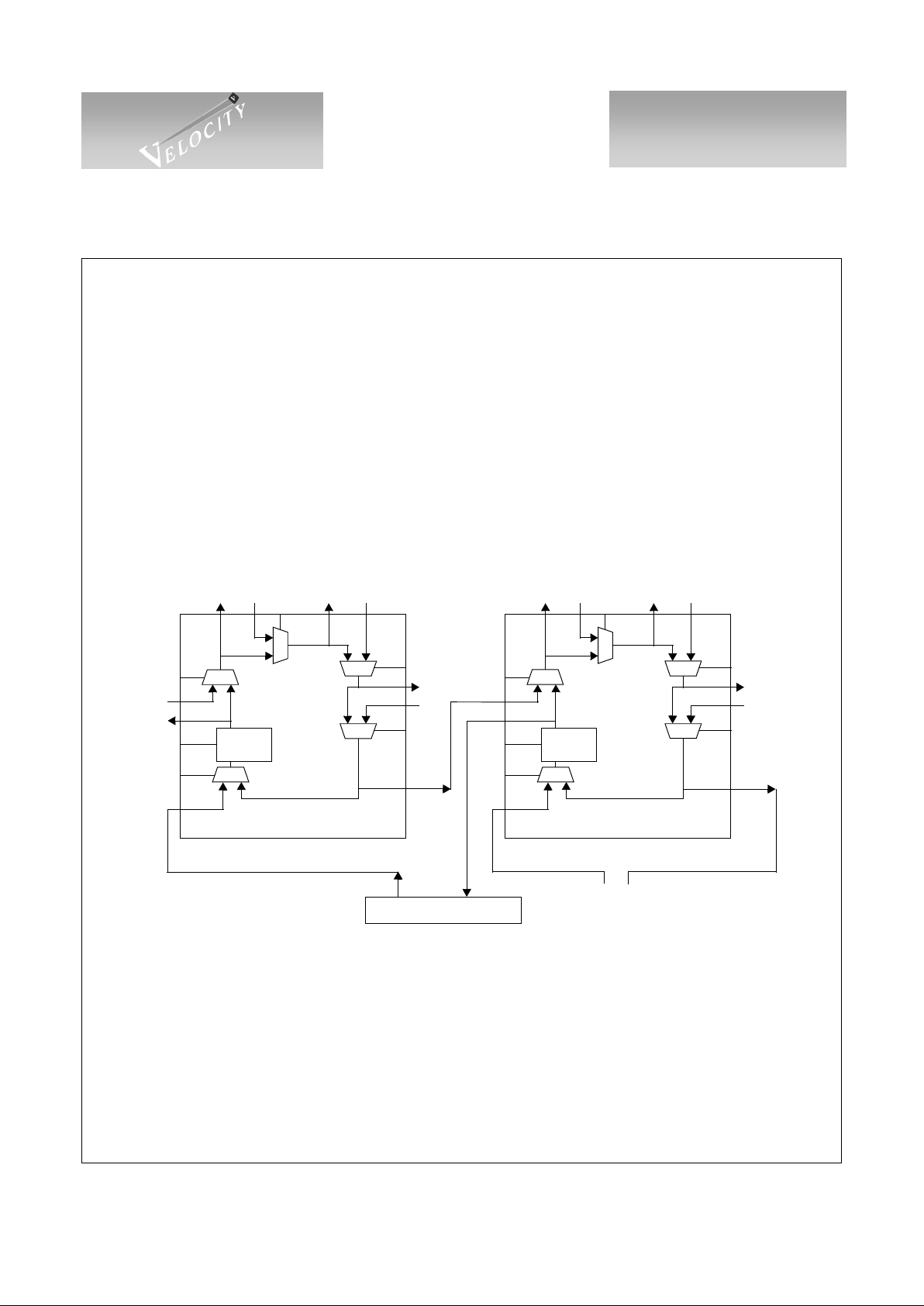
Application Example
Figure 2 shows one loop of an 8-drive JBOD implemented with two VSC712xs per loop. The input from
the connector goes through a repeater in order to clean up the signal prior to the array of disk drives. After all
eight PBCs, the output the to connector is retimed to ensure jitter compliance at the connector.
Figure 2: 8-Drive JBOD
1
0
SEL1
RPTR
1
0
1
0
1
0
I0
O0
I1
O1
I2
O2
I3O3
I4
O4
SEL4
SEL3
SEL2
MODE=0
SEL0=1
Drive 1
Drive 2
Drive 3
Drive 4
Connector
Drive 8
MODE
SEL0
1
0
1
0
SEL1
RTMR
1
0
1
0
1
0
I0
O0
I1
O1
I2
O2
I3O3
I4
O4
SEL4
SEL3
SEL2
MODE=1
SEL1=1
Drive 5
Drive 6
Drive 7
MODE
SEL0
1
0
1
1
0
1
NOT SHOWN: PBC5, SEL5
 Loading...