

VITESSE VSC7128QS Datasheet
VITESSE
SEMICONDUCTOR CORPORATION
Advance Product Information
SC7128
Features
• Supports ANSI X3T11 1.0625Gb/s FC-AL Disk
Attach for Resiliency
• Dual Repeaters (CRUs) Improve Signal Quality
• Six Port Bypass Circuits (PBCs) for Resiliency
• Dual Digital Signal Detect Units (SDUs)
Hex Port Bypass Circuit / Dual Repeater
for 1.0625 Gb/s FC-AL Disk Arrays
• Fully Differential for Minimum Jitter
• Selectable REFCLK: 53.125 / 106.25MHz
• TTL Bypass Select
• 3.3V Supply, 1.3W
• 64-Pin, 14 mm Thermally Enhanced PQFP
General Description
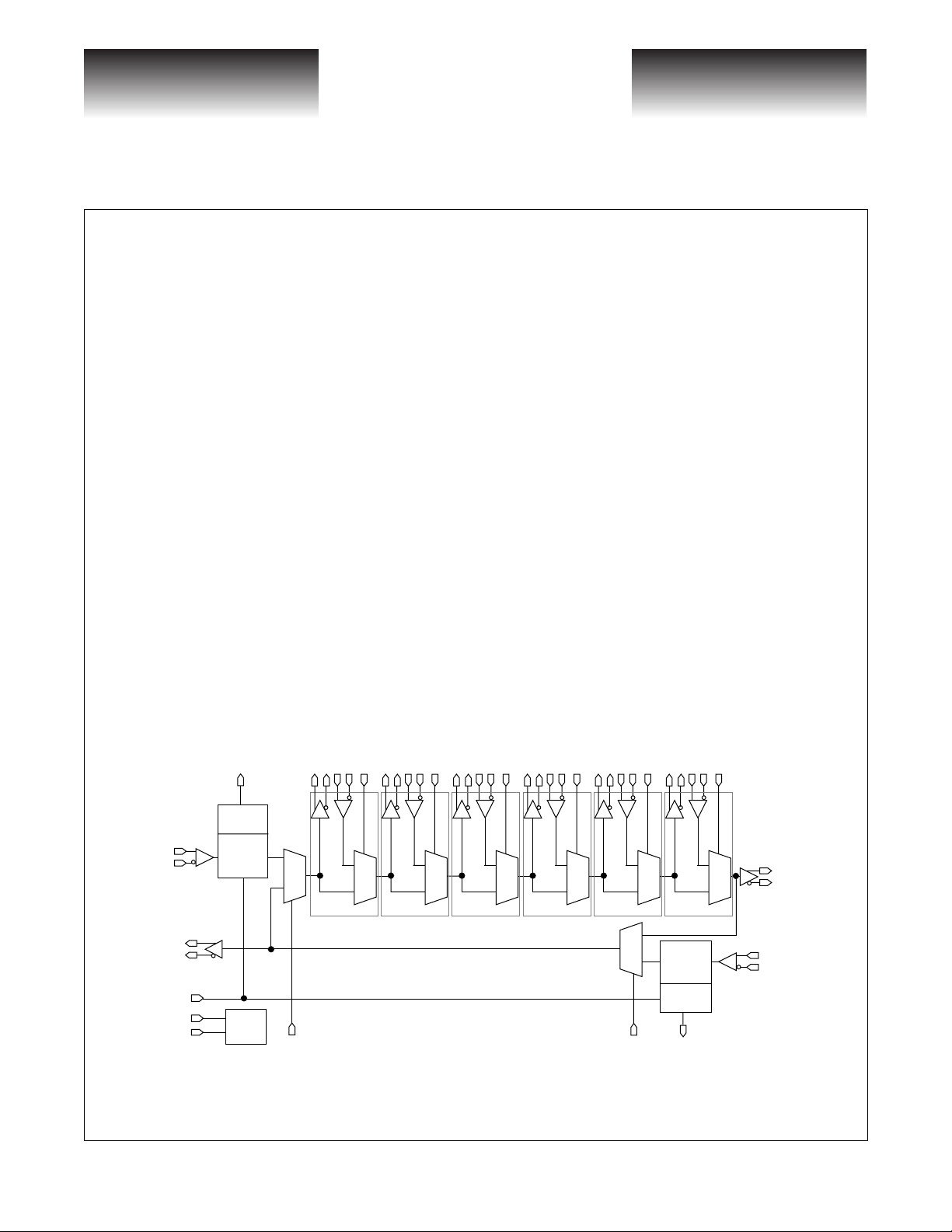
The VSC7128 contains six Port Bypass Circuits (PBCs), dual embedded Clock Recovery Unit repeaters
(CRU) and dual Signal Detect Units (SDU). These functions are inte grated into a single part to minimize circuit
size, part count, cost, high frequency routing and jitter accumulation. Together, they allow for optimized designs
of FC-AL JBOD systems that provide resiliency and hot insertion/removal of disk drives. The PBCs configure
the FC-AL loop to either include or exclude each drive. Repeaters retime the incoming signal thereby attenuating jitter so that downstream devices see high amplitude, low jitter signals. The SDUs determine whether the
output of the CRU is a valid Fibre Channel signal. Disk drives are connected directly to the LSO/LSI/SEL pins
while the IN/OUT pins can be connected to any FC-AL devices.
VSC7128 Block Diagram
FAIL1-
SDU1
Previous Device
IN1+
IN1-
OUT1+
OUT1-
CRU1
FAILSEL
RFSEL
REFCLK
(106/53 MHz)
CMU
MUX8
1
0
SEL8
DISK
DRIVE
#1
LSO1+
LSO1-
PBC1
LSI1+
LSI1-
1
0
SEL1
DISK
DRIVE
#2
LSO2+
LSO2-
PBC2
LSI2+
LSI2-
1
0
SEL2
DISK
DRIVE
#3
LSO3+
LSO3-
PBC3
LSI3+
LSI3-
1
0
SEL3
DISK
DRIVE
#4
LSO4+
LSO4-
PBC4
LSI4+
LSI4-
SEL4
1
0
PBC5
MUX7
DISK
DRIVE
#5
LSI5+
LSO5+
LSO5-
0
1
LSI5-
1
0
SEL7
SEL5
DISK
DRIVE
#6
LSO6+
LSO6-
PBC6
CRU2
SDU2
FAIL2-
LSI6+
LSI6-
1
0
SEL6
IN2+
IN2-
OUT2+
OUT2-
Next Device
G52177-0, Rev. 2.3
8/31/98 741 Calle Plano, Camarillo, CA 93012 • 805/388-3700 • FAX: 805/987-5896
VITESSE SEMICONDUCTOR CORPORATION Page 1

8
VITESSE
SEMICONDUCTOR CORPORATION
Hex Port Bypass Circuit / Dual Repeater
for 1.0625 Gb/s FC-AL Disk Arrays
Advance Product Information
Functional Description
A Port Bypass Circuit contains a differential 2:1 mux operating at 1.0625 Gb/s. The input to the PBC is
always passed to the LSOx output of the PBC to let the disk drive monitor loop activity. The mux selects either
the disk drive’s input, LSIx, or the input from the previous PBC as determined by the SELx input which is normally connected directly to the disk drives EN_BYP output. When SELx is HIGH, the mux selects the disk
drive input, LSIx. When SELx is LOW, the mux bypasses the disk drive input and passes the output of the previous PBC to the output of the PBC. Two extra muxes help route serial signals. MUX7 passes either the output
of PBC6 (bypass mode) or the output of CRU2 (normal mode) to MUX8/OUT1 depending whether SEL7 is
LOW or HIGH. MUX8 passes either the output of CRU1 or the output of MUX7 to PBC1 depending on
whether SEL8 is HIGH or LOW.
A TTL reference clock, REFCLK, is used by the internal Clock Multiplier Unit (CMU) to generate a baud
rate clock at 1.0625 Gb/s. If RFSEL is HIGH, the CMU multiplies REFCLK (nominally 106.25MHz) by a
factor of 10. If RFSEL is LOW, the CMU multiplies REFCLK (nominally 53.125MHz) by a factor of 20. The
user must ensure that RFSEL is properly set in order to match the frequency of REFCLK.
Two fully integrated Clock Recovery Units (CRUs) are provided to improve signal quality and determine
whether the input to the repeater is a valid Fibre Channel signal. Each repeater consists of a Clock Recovery
Unit (CRU) and a digital Signal Detect Unit (SDU). The CRU locks onto the incoming signal, generates a
recovered clock (at 1.0625 GHz) and uses this clock to resynchronize the incoming signal. The recovered data
has improved signal quality due to amplification and jitter attenuation. Recovered data is retimed to the recovered clock, not to REFCLK. The design of the CRU eliminates the need for an y Lock-to-Reference signal since,
in the absence of data, the CRU locks onto REFCLK automatically thereby eliminating the need for any external control circuitry.
The Signal Detect Units (SDUs) tests the output of the CRUs for valid Fibre Channel data by detecting run
length errors (more than 5 consecutive 1's or 0's) and the absence of a seven bit pattern found in the K28.5 character of either disparity (‘0000101’ or ‘1111010’). This K28.5 pattern should occur multiple times between
frames. The maximum length of a Fibre Channel frame is 2148 bytes (or 21,480 encoded bits) and the SDU
divides time into ~31 microsecond time intervals (2^15 bit times). At the end of each interval, any run length or
K28.5 errors which occurred during the interval are stored internally for use by the state machine which drives
the SDU output, FAILx-.
The FAILSEL input controls both SDUs and the FAILx- outputs provide the status of each SDU. FAILSEL
selects two different modes generated by the SDU; Single Frame (LOW) or Multiple Frame (HIGH) Error
Mode. In Single Frame Error Mode, any error condition that occurs within an interval causes FAILx- to be
asserted LOW immediately after that interval. FAILx- remains asserted until immediately after an error-free
interval occurs. In Multiple Frame Error Mode, FAILx- is asserted after four consecutive intervals containing
errors and remains asserted until four consecutive error-free intervals occur. The intent of the Multiple Frame
Error Mode is to allow FAIL1- or FAIL2- to be directly connected to the mux controls, SEL8 or SEL7, in order
to configure the part to isolate IN1 or IN2 whenever valid data is not present. Single Frame Error Mode allows
the user to develop their own algorithm for monitoring data and controlling MUX8 or MUX7.
VSC712
Page 2
VITESSE SEMICONDUCTOR CORPORATION
741 Calle Plano, Camarillo, CA 93012 • 805/388-3700 • FAX: 805/987-5896 8/31/98
G52177-0, Rev. 2.3

VITESSE
SEMICONDUCTOR CORPORATION
Advance Product Information
SC7128
AC Characteristics
Figure 1: AC Timing Diagrams
INx+/-,
LSIx+/-
LSOx+/-,
OUTx+/-
T
p
REFCLK
T
t
Table 1: AC Characteristics
(Over recommended operating conditions).
Hex Port Bypass Circuit / Dual Repeater
for 1.0625 Gb/s FC-AL Disk Arrays
80%
20%
T
p
T
h
T
t
T
l
T
s
V
IH(MIN)
V
IL(MAX)
T
T
s
Parameters
T
p
T
s
T
t
F REFCLK Frequency
T REFCLK Period
F
o
DC REFCLK Duty Cycle 35 65 % Measured at 1.5V
T
, T
h
l
Description Min. Max. Units Conditions
Differential Inputs/Outputs
Latency from IN, LSI to LSO,
OUT
Differential Output Rise/Fall time — 300 ps
Reference Clock Requirements
REFCLK input rise/fall times — 2.0 ns Between V
Frequency Offset -200 +200 ppm
REFCLK Input HIGH/LOW time 2.5 — ns.
0.25 7.0 ns 75 Ohm Load
Between 20% and 80%
Tested on a sample basis
106.25 MHz Nominal if RFSEL is
105
52.5
9.2
18.5
108
54
9.53
19.0
MHz
ns
HIGH
53.125 MHz Nominal if RFSEL is
LOW
RFSEL = HIGH
RFSEL = LOW
Maximum frequency offset between
10 or 20 times REFCLK and the data
rate of the serial input to the CRU.
From V
IL(min)
to V
IL(max)
IL(MAX)
to V
and V
IH(min)
IH(MIN)
or V
IH(max)
G52177-0, Rev. 2.3
8/31/98 741 Calle Plano, Camarillo, CA 93012 • 805/388-3700 • FAX: 805/987-5896
VITESSE SEMICONDUCTOR CORPORATION Page 3
 Loading...