

VITESSE VSC7125QU, VSC7125QN Datasheet
VITESSE
SEMICONDUCTOR CORPORATION
Data Sheet
SC7125
1.0625 Gbits/sec Fibre
Channel Transceiver
Features
• ANSI X3T11 Fibre Channel Compatible
1.0625 Gbps Full-duplex Transceiver
• 10 Bit TTL Interface for Transmit and
Receive Data
• Monolithic Clock Synthesis and Clock
Recovery - No External Components
• 106.25 MHz TTL Reference Clock
• Low Power Operation - 650 mW
• Suitable for Both Coaxial and Optical
Link Applications
• 64 Pin, 10mm or 14mm PQFP
• Single +3.3V Power Supply
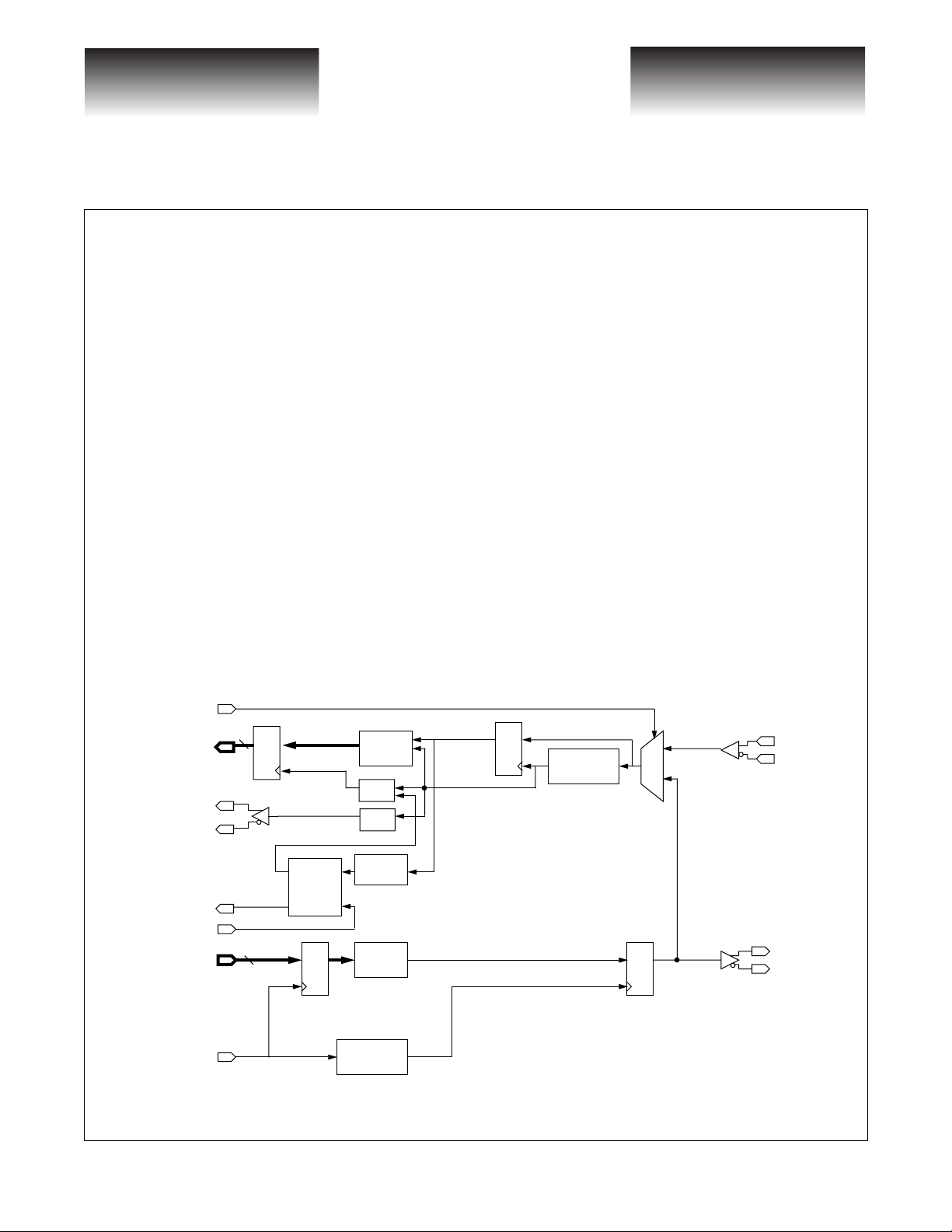
General Description
The VSC7125 is a full-speed Fibre Channel Transceiver optimized for Disk Drive and other space constrained applications. It accepts 10-bit 8B/10B encoded transmit data, latches it on the rising edge of REFCLK
and serializes it onto the TX PECL differential outputs at a baud rate which is ten times the REFCLK frequency.
The VSC7125 also samples serial receive data on the RX PECL differential inputs, recovers the clock and data,
deserializes it onto the 10-bit receive data bus, outputs two recovered clocks at one twentieth of the incoming
baud rate and detects Fibre Channel “Comma” characters. The VSC7125 contains on-chip PLL circuitry for
synthesis of the baud-rate transmit clock, and extraction of the clock from the received serial stream. These circuits are fully monolithic and require no external components.
VSC7125 Block Diagram
EWRAP
R0:9
RCLK
RCLKN
COM_DET
EN_CDET
T0:9
REFCLK
10
Resync
10
Q D
Frame
Logic
D Q
PLL Clock
Multiply
Serial to
Parallel
÷ 10
÷ 20
Comma
Detect
Parallel
to Serial
Retimed
Data
Recovered
Clock
Q D
Recovery
Serial Data
Synthesized
Clock
Clock
D Q
2:1
RX+
RX-
TX+
TX-
G52121-0, Rev. 4.1
4/23/98 741 Calle Plano, Camarillo, CA 93012 • 805/388-3700 • FAX: 805/987-5896
VITESSE
SEMICONDUCTOR CORPORATION
Page 1
VITESSE
SEMICONDUCTOR CORPORATION
.0625 Gbits/sec Fibre
hannel Transceiver
Data Sheet
VSC7125
Functional Description
Clock Synthesizer
The VSC7125 clock synthesizer multiplies the reference frequency provided on the REFCLK pin by 10 to
achieve a baud rate clock at nominally 1.0625 GHz. The clock synthesizer contains a fully monolithic PLL
which does not require any external components.
Serializer
The VSC7125 accepts TTL input data as a parallel 10 bit character on the T0:9 b us which is latched into the
input latch on the rising edge of REFCLK. This data will be serialized and transmitted on the TX PECL differential outputs at a baud rate of ten times the frequency of the REFCLK input, with bit T0 transmitted first. User
data should be encoded for transmission using the 8B/10B block code described in the Fibre Channel specification, or an equivalent, edge rich, DC-balanced code.
Transmission Character Interface
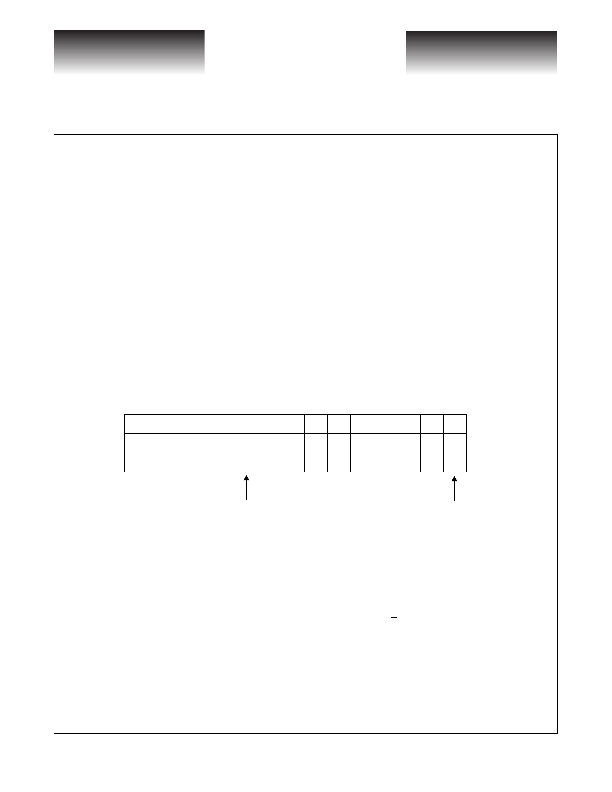
In Fibre Channel, an encoded byte is 10 bits and is referred to as a transmission character. The 10 bit interface on the VSC7125 corresponds to a transmission character. This mapping is illustrated below.
Figure 1: Transmission Order and Mapping to Fibre Channel Character
Parallel Data Bits
8B/10B Bit Position
Comma Character
Last Data Bit Transmitted
Clock Recovery
The VSC7125 accepts differential high speed serial inputs on the RX+/RX- pins, extracts the clock and
retimes the data. The serial bit stream should be encoded to provide DC balance and limited run length by a
Fibre Channel compatible 8B/10B transmitter or equivalent. The VSC7125 clock recovery circuitry is completely monolithic and requires no external components. For proper operation, the baud rate of the data stream
to be recovered should be within 0.01% of ten times the REFCLK frequency. For example if the REFCLK used
is 106.25MHz, then the incoming serial baud rate must be 1.0625 gigabaud +
Deserializer
The retimed serial bit stream is converted into a 10-bit parallel output character. The VSC7125 provides
complementary TTL recovered clocks, RCLK and RCLKN, which are at one twentieth of the serial baud rate.
This architecture is designed to simplify demultiplexing of the 10-bit data characters into a 20-bit halfword in
the downstream controller chip. The clocks are generated by di viding do wn the high-speed clock which is phase
locked to the serial data. The serial data is retimed by the internal high-speed clock, and deserialized. The
T9 T8 T7 T6 T5 T4 T3 T2 T1 T0
j hgfi edcba
XXX1111100
First Data Bit Transmitted
0.01%.
Page 2
VITESSE
741 Calle Plano, Camarillo, CA 93012 • 805/388-3700 • FAX: 805/987-5896 4/23/98
SEMICONDUCTOR CORPORATION
G52121-0, Rev. 4.1
VITESSE
SEMICONDUCTOR CORPORATION
Data Sheet
SC7125
resulting parallel data will be captured by the adjoining protocol logic on the rising edges of RCLK and
RCLKN. In order to maximize the setup and hold times available at this interface, the parallel data is loaded
into the output register at a point nominally midway between the transition edges of RCLK and RCLKN.
If serial input data is not present, or does not meet the required baud rate, the VSC7125 will continue to
produce a recovered clock so that downstream logic may continue to function. The RCLK and RCLKN output
frequency under these circumstances may differ from their expected frequency by no more than +
Word Alignment
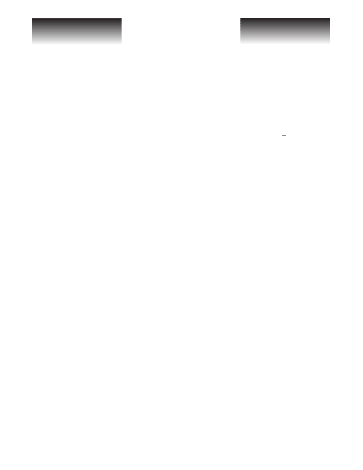
The VSC7125 provides 7-bit Fibre Channel comma character recognition and data word alignment. Word
synchronization is enabled by asserting EN_CDET HIGH. When synchronization is enabled, the VSC7125 constantly examines the serial data for the presence of the Fibre Channel “comma” character. This pattern is
“0011111XXX”, where the leading zero corresponds to the first bit received. The comma sequence is not contained in any normal 8B/10B coded data character or pair of adjacent characters. It occurs only within special
characters, known as K28.1, K28.5 and K28.7, which is defined specifically for synchronization in Fibre Channel systems. Improper alignment of the comma character is defined as any of the following conditions:
1) The comma is not aligned within the 10-bit transmission character such that T0...T6 = “0011111”
2) The comma straddles the boundary between two 10-bit transmission characters.
3) The comma is properly aligned but occurs in the received character presented during the rising edge of
RCLK rather than RCLKN.
When EN_CDET is HIGH and an improperly aligned comma is encountered, the internal data is shifted in
such a manner that the comma character is aligned properly in R0:9. This results in proper character and halfword alignment. When the parallel data alignment changes in response to an improperly aligned comma pattern,
some data which would have been presented on the parallel output port may be lost. However, the synchronization character and subsequent data will be output correctly and properly aligned. When EN_CDET is LOW, the
current alignment of the serial data is maintained indefinitely, regardless of data pattern.
On encountering a comma character, COM_DET is driven HIGH to inform the user that realignment of the
parallel data field may have occurred. The COM_DET pulse is presented simultaneously with the comma character and has a duration equal to the data, or half of an RCLK period. The COM_DET signal is timed such that
it can be captured by the adjoining protocol logic on the rising edge of RCLKN. Functional waveforms for synchronization are given in Figure 2 and Figure 3. Figure 2 shows the case when a comma character is detected
and no phase adjustment is necessary . It illustrates the position of the COM_DET pulse in relation to the comma
character on R0:9. Figure 3 shows the case where the K28.5 is detected, but it is out of phase and a change in
the output data alignment is required. Note that up to three characters prior to the comma character may be corrupted by the realignment process.
1.0625 Gbits/sec Fibre
Channel Transceiver
1%.
G52121-0, Rev. 4.1
4/23/98 741 Calle Plano, Camarillo, CA 93012 • 805/388-3700 • FAX: 805/987-5896
VITESSE
SEMICONDUCTOR CORPORATION
Page 3
VITESSE
SEMICONDUCTOR CORPORATION
.0625 Gbits/sec Fibre
hannel Transceiver
Figure 2: Detection of a Properly Aligned Comma Character
RCLK
RCLKN
COM_DET
R0:9
TChar: 10 bit Transmission Character
Data Sheet
VSC7125
K28.5 TChar TChar TChar
Figure 3: Detection and Resynchronization of an Improperly Aligned Comma
RCLK
RCLKN
COM_DET
R0:9
Receiving Two Consecutive K28.5+TChar Transmission Words
K28.5 TChar TChar TChar K28.5 TChar
Potentially Corrupted
Page 4
VITESSE
741 Calle Plano, Camarillo, CA 93012 • 805/388-3700 • FAX: 805/987-5896 4/23/98
SEMICONDUCTOR CORPORATION
G52121-0, Rev. 4.1
VITESSE
SEMICONDUCTOR CORPORATION
Data Sheet
SC7125
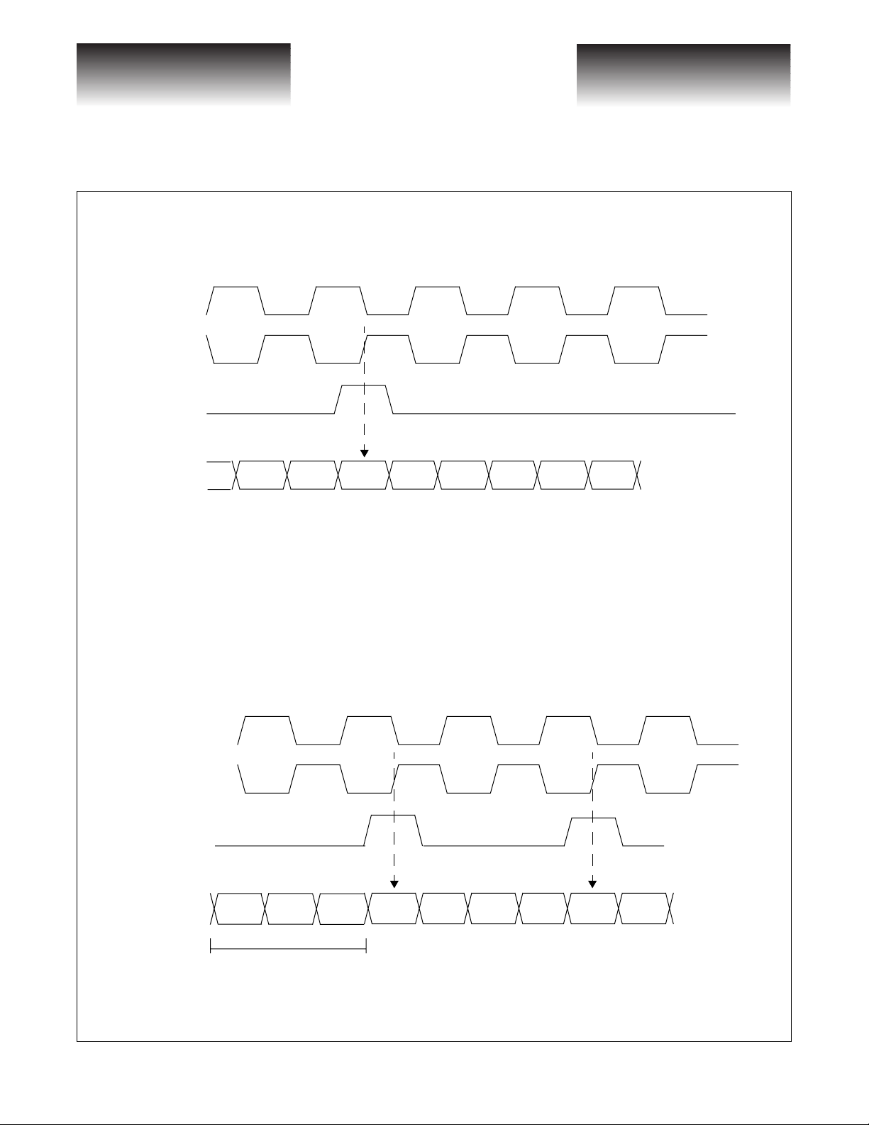
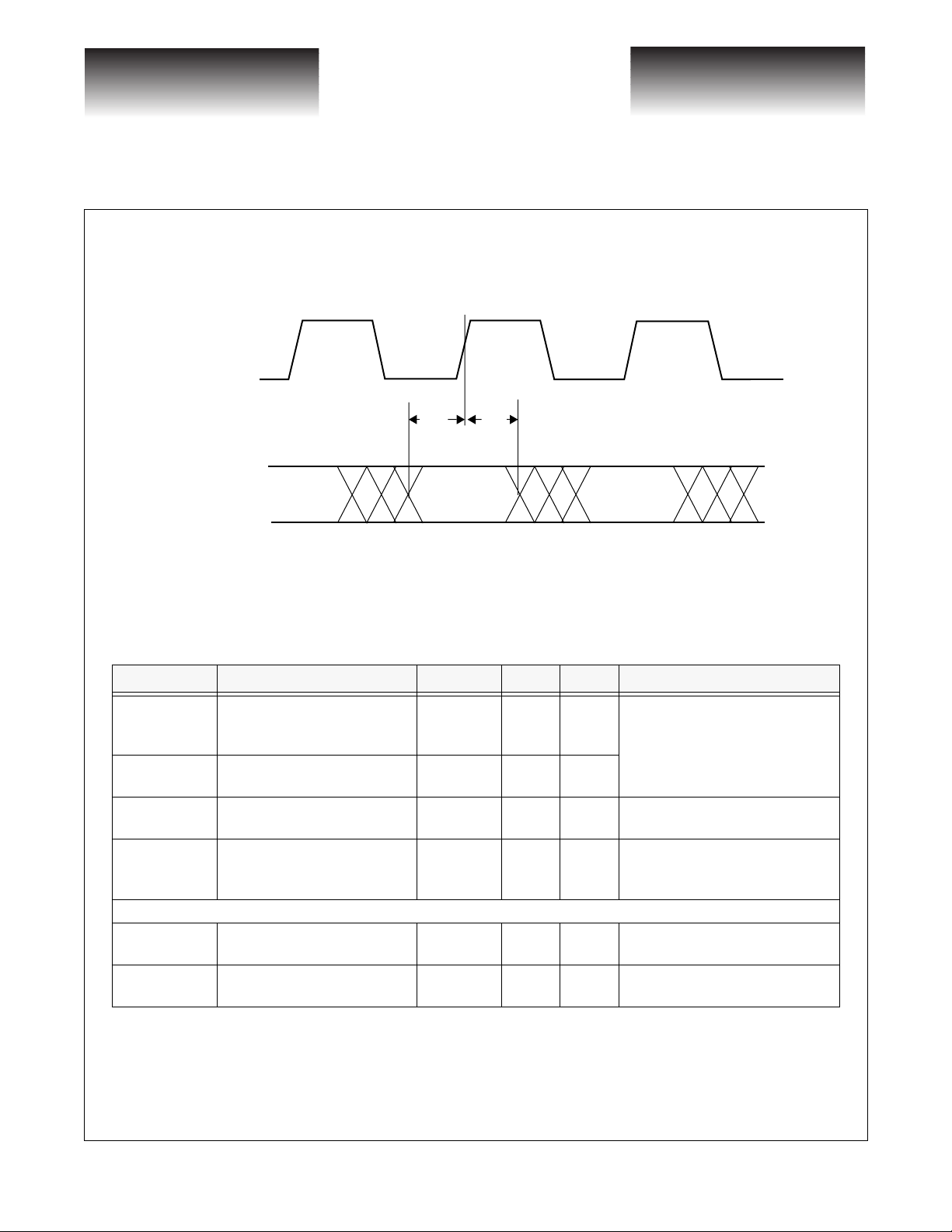
REFCLK
T0:9
10 Bit Data
AC Characteristics
Data V alid
Figure 4: Transmit Timing W aveforms
T
1
Data V alid
T
2
1.0625 Gbits/sec Fibre
Channel Transceiver
Data V alid
Table 1: Transmit AC Characteristics
Parameters
T
1
T
2
T
,T
SDR
SDF
T
LAT
T
rj
T
DJ
T0:9 Setup time to the rising
edge of REFCLK
T0:9 hold time after the
rising edge of REFCLK
TX+/TX- rise and fall time
Latency from rising edge of
REFCLK to T0 appearing on
TX+/TX-
Serial data output random
jitter (RMS)
Serial data output
deterministic jitter (p-p)
Description Min Max Units Conditions
Transmitter Output Jitter Allocation
1.5 — ns.
1.0 — ns.
— 300 ps.
11bc - 1ns ns.
— 20 ps.
— 100 ps.
Measured between the valid
data level of T0:9 to the 1.4V
point of REFCLK
20% to 80%, 75 Ohm load to
Vss, Tested on a sample basis
bc = Bit clocks
ns = Nano second
RMS, tested on a sample basis
(refer to Figure 8)
Peak to peak, tested on a sample
basis (refer to Figure 8)
G52121-0, Rev. 4.1
4/23/98 741 Calle Plano, Camarillo, CA 93012 • 805/388-3700 • FAX: 805/987-5896
VITESSE
SEMICONDUCTOR CORPORATION
Page 5
 Loading...