

VITESSE VSC7124QM Datasheet
VITESSE
SEMICONDUCTOR CORPORATION
Advance Product Information
VSC7124
Quad Port Bypass Circuit
Features
• ANSI X3T11 Fibre Channel Compliant at 1.0625Gb/s
• IEEE 802.3z Gigabit Ethernet Compliant at 1.25Gb/s
• Five Port Bypass Circuits (PBCs)
• On-Chip Transmit Termination
General Description
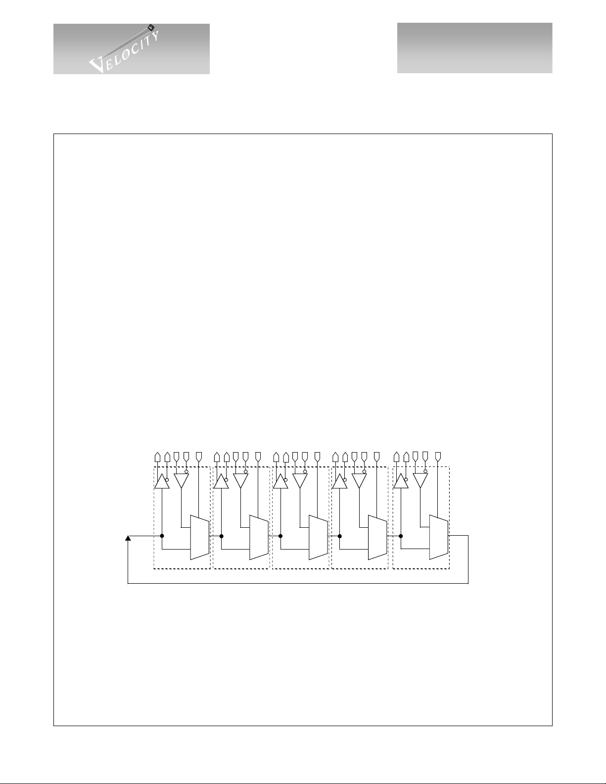
The VSC7124 contains five cascaded Port Bypass Circuits (PBCs) used to steer serial signals. This part is typically used in distribu ting Fibre C hannel signals t o an ar ray of disk dr ives in a n FC-A L loo p as il lustrat ed in Figure 1. The VSC7124 can b e used with an y of the Vitesse JBOD circuits to implem ent FC-AL JBODs of
virtually any size. In Figure 1, the first VSC7127’s CRU is configured as a Repeater to attenuate jitter. The
VSC7124 does not contain a CR U in order to reduce po wer and co st. The second VSC712 7’s CRU is configured as a retimer so that the output of the device is a jitter compliance point.
Each PBC is a multiplexer that is controlled by the corresponding SELx line which, if HIGH, selects the external input or, if LOW, selects the output of the previous PBC.
VSC7124 Block Diagram
• 3.3V, 0.25W Typical Power
• 0.35um CMOS, a Velocity Family Member
• 44-Pin, 10mm PQFP Package
O1-
O1+
PBC1
I1+
I1-
I0+
O0-
I0-
SEL0
1
0
SEL1
1
0
O2+
O2-
PBC2
I2+
I2-
SEL2
1
0
O3+
O3-
PBC3
I3+
I3-
1
0
SEL3
O4+
O4-
PBC4
I4+
I4-
O0+
SEL4
1
0
PBC0
G52293-0, Rev 2.3 Page 1
05/07/01
© VITESSE SEMICONDUCTOR CORPORATION • 741 Calle Plano • Camarillo, CA 93012
Tel: (800) VITESSE • FAX: (805) 987-5896 • Email: prodinfo@vitess e.com
Internet: www.vitesse.com
VITESSE
SEMICONDUCTOR CORPORATION
Advance Product Information
Quad Port Bypass Circuit
VSC7124
Application Example
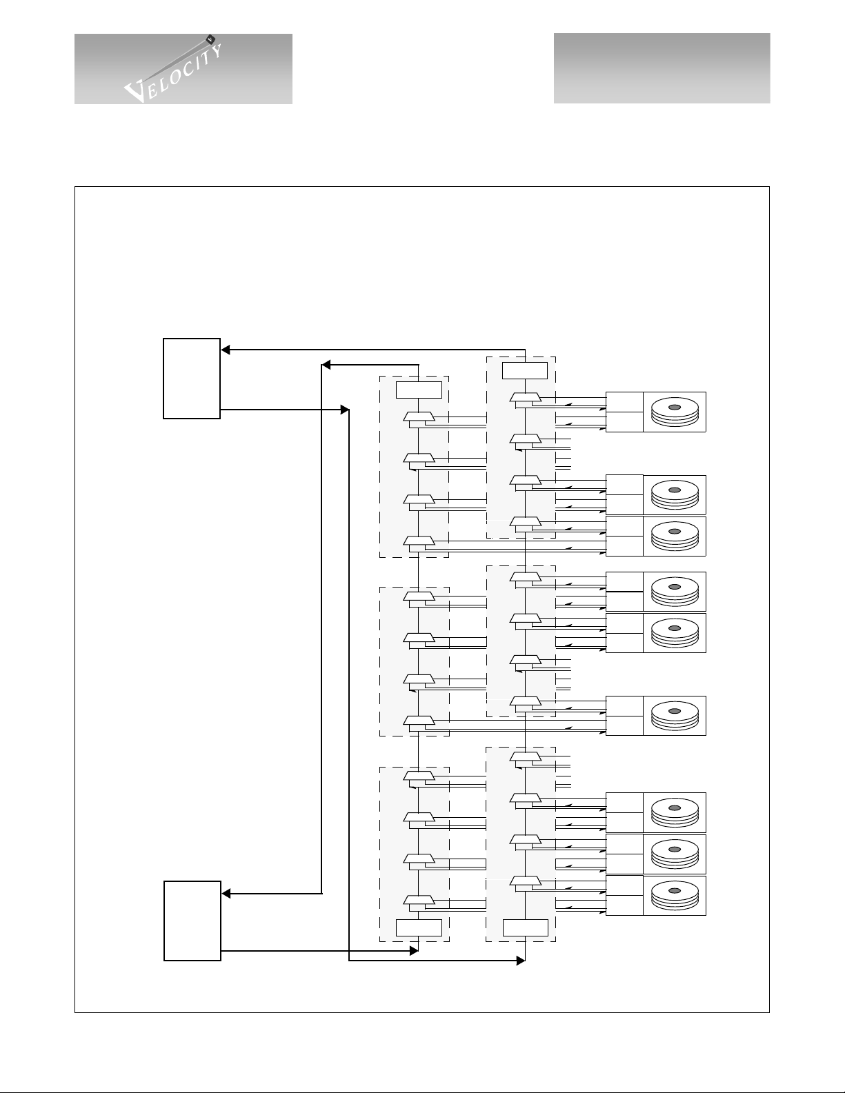
A 12-port JBOD is shown in Figure 1. This dual l oop ap pli cat i on use s one VSC 7127 R, on e VSC7127T and one
VSC7124 on each loop in order to configure the FC-AL disk arr ay. Functional drives are included in the FCAL loop while nonfunctional or missing drives (numbers 2, 7, 9) are excluded.
Figure 1: 12-Drive FC-AL JBOD Application
Optics
or
Copper
LOOP A
CONFIGURATION:
VSC7127R #1 & 2: Repeater Mode
SEL0=1, SEL5=1
MODE=0
VSC7124 #3 & 4: No CRU
VSC7127T #5 & 6: Retimer Mode
SEL1=1, SEL5=1
MODE=1
Optics
or
Copper
LOOP B
1
Retimer
10
0
1
0
0
4
1
3
VSC7127T #5
1
0
0
0
VSC7121 QUAD PORT BYPASS CIRCUIT
VSC7124 #3
0
0
VSC7127R #1
Repeater
2
1
0
1
4
1
3
10
2
10
1
0
0
10
4
10
3
1
2
1
1
0
Retimer
0
0
0
VSC7127T #6
VSC7124 #4
0
0
0
0
VSC7127R #2
Repeater
1
1
1
10
10
10
10
1
1
1
1
10
7125
SerDes
7125
SerDes
7125
SerDes
7125
SerDes
7125
SerDes
7125
SerDes
7125
SerDes
7125
SerDes
7125
SerDes
7125
SerDes
7125
SerDes
7125
SerDes
7125
SerDes
7125
SerDes
7125
SerDes
7125
SerDes
7125
SerDes
7125
SerDes
1
2
3
4
5
6
7
8
9
10
11
12
Page 2 G52293-0, Rev 2.3
© VITESSE SEMICONDUCTOR CORPORATION • 741 Ca l le Pl an o • Camarillo, CA 93012
Tel: (800) VITESSE • FAX: (805) 987-5896 • Email: prodinfo@vitesse.com
Internet: www.vitesse.com
5/7/01
VITESSE
SEMICONDUCTOR CORPORATION
Advance Product Information
VSC7124
Quad Port Bypass Circuit
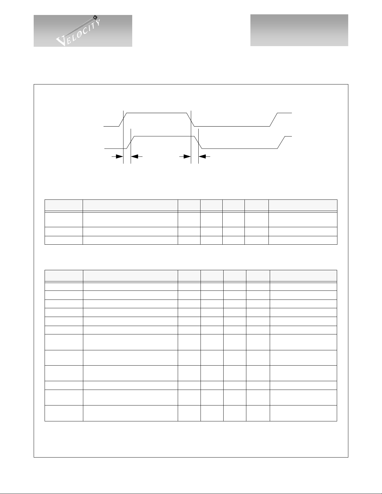
Figure 2: Timing Waveforms
Ix+/-
Ox+/-
T
1
T
1
AC Characteristics (Over Recommended Operating Conditions)
Parameters Description Min Typ Max Units Conditions
T
1
T
R
T
j(PBC)
, T
Propagation Delay 7.0 ns
F
Serial Data Rise and Fall Time 300 ps At ∆VIN minimum leve l s
Data Jitter Accummulation 120 ps Peak-to-Peak on Ox+/-
Delay with all circuits
bypassed.
DC Characteristics (Over Recommended Operating Conditions)
Parameters Description Min Typ Max Units Conditions
V
OH
V
OL
V
IH
V
IL
I
IH
I
IL
∆V
OUT75
∆V
OUT50
(1)
∆V
IN
V
DD
P
D
I
DD
NOTE: (1) Refer to Application Note AN-37 for details regarding differential voltage measurements.
Output HIGH voltage (TTL) 2.4 V IOH = -1.0 mA
Output LOW voltage (TTL) 0.5 V IOL = +1.0 mA
Input HIGH voltage (TTL) 2.0 5.5 V
Input LOW voltage (TTL) 0 0.8 V
Input HIGH current (TTL) 50 500 µAVIN =2.4V
Input LOW current (TTL) -500 µAVIN =0.5V
TX output differential peak-to-peak
(1)
voltage swing
TX output differential peak-to-peak
(1)
voltage swing
Receiver differential peak-to-peak
Input Sensitivity RX
Supply voltage 3.14 3.47 V 3.3V±5%
Power dissipation 250 555 mW
Power Supply Current 76 160 mA
1200 2200 mVp-p 75Ω to V
1000 2200 mVp-p 50Ω to VDD – 2.0 V
400 2600 mVp-p Internally biased to V
– 2.0 V
DD
Outputs open,
= VDD max ±2%
V
DD
Outputs open,
= VDD max
V
DD
DD
/2
G52293-0, Rev 2.3 Page 3
05/07/01
© VITESSE SEMICONDUCTOR CORPORATION • 741 Calle Plano • Camarillo, CA 93012
Tel: (800) VITESSE • FAX: (805) 987-5896 • Email: prodinfo@vitesse.com
Internet: www.vitesse.com
 Loading...