

V
E
L
O
C
I
T
Y
T
M
VITESSE
SEMICONDUCTOR CORPORATION
Advance Product Information
VSC7123 - Extended Temperature Range
10-Bit Transceiver for Fibre
Channel and Gigabit Ethernet
G52312-0, Rev 2.2 Page 1
04/05/01
© VITESSE SEMICONDUCTOR CORPORATION • 741 Calle Plano • Camarillo, CA 93012
Tel: (800) VITESSE • FAX: (805) 987-5896 • Email: prodinfo@vitesse.com
Internet: www.vitesse.com
Features
General Description
The VSC7123 Extended Temperature Range (ETR) is a full-speed Fibre Channel and Gigabit Ethernet
Transceiver with industry-standard pinouts, which operates down to
−40
o
. The VSC7123 ETR accepts 10-bit
8B/10B encoded transmit data, latches i t on the ri sin g edge of REFCLK and seri ali zes i t onto the TX PEC L differential outputs at a ba ud rate wh ich is 10 t imes the REFCLK frequenc y. Serial da ta input on the RX PEC L differential inputs is resampled by the Clock Recovery Unit (CRU) and deserialized onto the 10-bit receive data
bus synchronously to complementary divide-by-twenty clocks. The VSC7123 ETR receiver detects “Comma”
characters for frame alignment. An analog/digital signal detection circuit indicates that a valid signal is present
on the RX input. A cable equalizer compensates for InterSymbol Interference (ISI) in order to increase maximum cable distances.
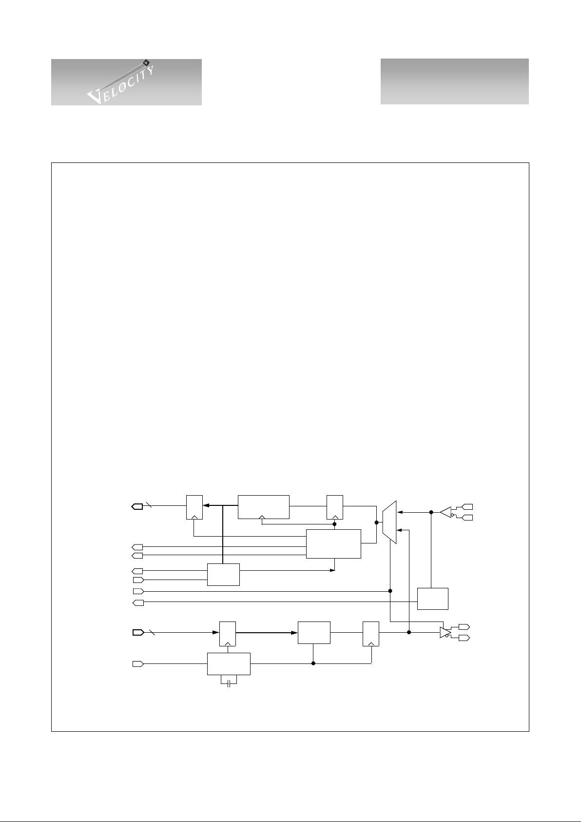
VSC7123 ETR Block Diagram
• 802.3z Gigabit Ethernet Compliant 1. 25 Gb/ s
Transceiver
• ANSI X3T11 Fibre Channel Compliant
1.0625 Gb/s Transceiver
• 0.98 Gb/s to 1.36 Gb/s Ful l -Dupl ex Oper ati on
• 10-Bit TTL Interface for Transmit and
Receive Data
• Operating Temperature Down to -40
o
• RX Cable Equalization
• Analog/Digital Signal Detection
• JTAG Access Port for Testability
• 64-Pin, 10 mm TQFP Package
• Single +3.3V Supply, 650mW Typical
RX+
RX-
Q D
Serial to
Parallel
Clock
Recovery
÷10
Comma
R(0:9)
COMDET
ENCDET
T(0:9)
x10 Clock
Multiply
Parallel
to Serial
TX+
TX-
EWRAP
÷20
RCLK
10
10
2:1
RCLKN
REFCLK
Signal
Detect
Q D
QD
Detect
SIGDET
D QD Q
NOT SHOWN: JTAG Boundary Scan

V
E
L
O
C
I
T
Y
T
M
VITESSE
SEMICONDUCTOR CORPORATION
Advance Product Information
10-Bit Transceiver for Fibre
Channel and Gigabit Ethernet
Extended Temperature Ra nge - VSC7123
Page 2 G52312-0, Rev 2.2
04/05/01
© VITESSE SEMICONDUCTOR CORPORATION • 741 Ca ll e Pl an o • Camarillo, CA 93012
Tel: (800) VITESSE • FAX: (805) 987-5896 • Email: prodinfo@vitesse.com
Internet: www.vitesse.com
Functional Description
Clock Synthesizer
The VSC7123 ETR clock synthesizer multiplies the reference frequency provided on the REFCLK pin by
10 to achieve a baud rate clock be tween 0.98GH z and 1.36GHz. The on-chip Pha se Lock Loop (PLL) use s a
single external 0.1
µF capacitor to control the Loop Filter.
Serializer
The VSC7123 ETR accepts TTL input data as a parallel 10 bit character on the T(0:9) bus, which is latched
into the input register on the rising edge of REFCLK. This data is serialized and transmitted on the TX PECL
differential outputs at a baud rate that is 10 times the frequency of the REFCLK, with bit T0 transmitted first.
User data should be encoded using 8B/10B block code or equivalent.
Transmission Character Interface
An encoded byte is 10 bits and is referred to as a transmission character. The 10-bit interface on the
VSC7123 ETR corresponds to a transmission character. This mapping is shown in Figure 1.
Figure 1: Transmission Order and Mapping of an 8B/10B Character
Clock Recovery
The VSC7123 ETR accepts differential high-speed serial inputs on the RX+/RX- pin s, extracts the clock
and retimes the data. Equalizers are included in the receiver to open the data eye and compensate for InterSymbol Interference which may be pres ent in the incoming data. The se rial bit stream should be encoded so as to
provide DC balance and limited run length by an 8B/10B encoding scheme. The CRU is completely monolithic
and requires no external components. For proper operation, the baud rate of the data stream to be recovered
should be within +
200ppm of 10 times the REFCLK frequency. For example, Gigabit Ethernet systems would
use 125MHz oscillators with a
±100ppm accuracy resulting in ±200ppm between VSC7123 ETR pairs.
Deserializer
The recovered serial bit stream is converted into a 10-bit parallel output character. The VSC7123 ETR provides complementary TTL recovered clocks, RCLK and RCLKN, which are 1/20
th
of the serial baud rate. The
clocks are generated by dividing down the high-speed recovered clock which is phase-locked to the serial data.
The serial data is retimed, deserialized and out pu t on R(0 :9). T he paral lel dat a wil l be capture d by the adj oi ni ng
protocol logic on the rising edges of RCLK and RCLKN.
First Data Bit Transmitted
Last Data Bit Transmitted
Parallel Data Bits
8B/10B Bit Position
T9 T8 T7 T6 T5 T4 T3 T2 T1 T0
j hgfi edcba
Comma Character
XXX1111100

V
E
L
O
C
I
T
Y
T
M
VITESSE
SEMICONDUCTOR CORPORATION
Advance Product Information
VSC7123 - Extended Temperature Range
10-Bit Transceiver for Fibre
Channel and Gigabit Ethernet
G52312-0, Rev 2.2 Page 3
04/05/01
© VITESSE SEMICONDUCTOR CORPORATION • 741 Calle Plano • Camarillo, CA 93012
Tel: (800) VITESSE • FAX: (805) 987-5896 • Email: prodinfo@vitesse.com
Internet: www.vitesse.com
If serial input data is not present, or does not meet the required baud rate, the VSC7123 ETR will continue
to produce a recovered clo ck, a ll owing downstream logic functionalilty t o co nt in ue. T he RCLK/ RCLKN output
frequency under these circumstances will differ from its expected frequency by no more than +
1%.
Word Alignment
The VSC7123 ETR provides 7-bit comma character rec ogni tio n an d dat a wo rd al ignment . Word synchron ization is enabled by asserting ENCDET HIGH. When synchronization is enabled, the receiver examines the
recovered serial data for the presence of the “Comma” character. This pattern is “0011111XXX”, where the
leading zero corresponds to the first bit received. The comma sequence is not contained in any normal 8B/10B
coded data character or pair of adjacent characters. It occurs only within special characters, known as K28.1,
K28.5 and K28.7, which are defined for synchronization purposes. Improper alignment of the “Comma” character is defined as any of the following conditions:
1) The comma is not aligned within the 10-bit transmission character such that R0...R6 = “0011111”.
2) The comma straddles the boundary between two 10-bit transmission characters.
3) The comma is properly aligned but occurs in the received character presented during the rising edge of
RCLK rather than RCLKN.
When ENCDET is HIGH and an improperly aligned comma is encountered, the recovered clock is
stretched (never slivered) so that the comma character and recovered clocks are properly aligned to R(0:9). This
results in proper character and word alignment. When the parallel data alignment changes in response to an
improperly aligned comma p att er n, some d a ta whi ch wo ul d have been presented on the paral le l out put p ort may
be lost. Additionally, the first Comma patt er n may also b e lo st or co rru pt ed. Su bsequent data will be output correctly and properly aligned. When ENCDET is LOW, the current alignment of the serial data is maintained
indefinitely, regardless of data pattern.
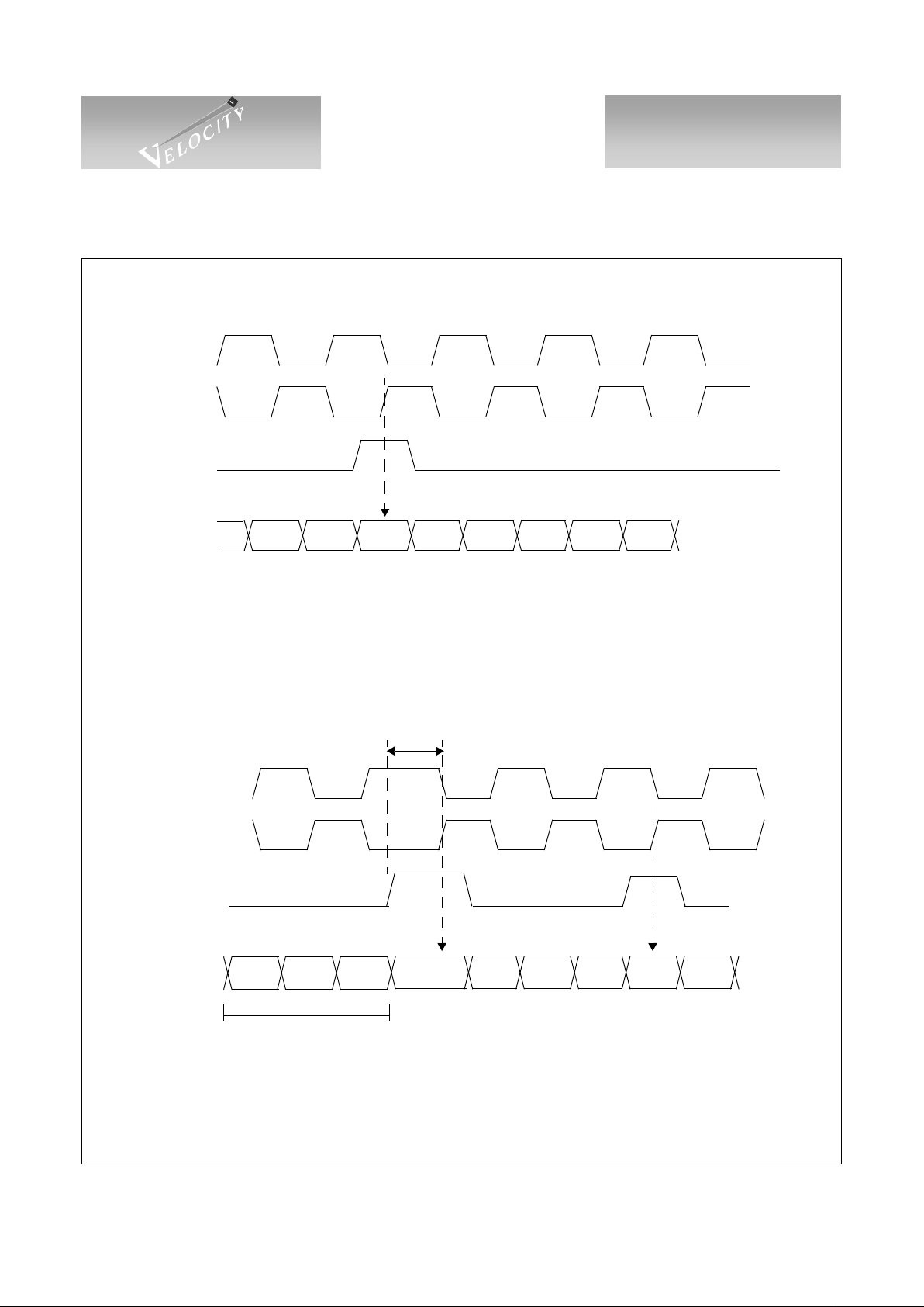
On encountering a comma character, COMDET is driven HIGH. The COMDET pulse is presented simultaneously with the comma charact er and has a duration equal to the dat a, or ha lf of an R CLK per iod. The COMDET signal is timed such that it can be captured by the adjoining protocol logic on the rising edge of RCLKN.
Functional waveforms for synchronization are given in Figure 2 and Figure 3. Figure 2 shows the case when a
comma character is detected and no phase adjust ment is necessary. It illustrates the position of the COMDET
pulse in relation to the comma character on R(0:9). Figure 3 shows the case where the K28.5 is detected, but it
is misaligned so a change in the output data alignment is required. Note that up to three characters prior to the
comma character may be corrupted by the realignment process.
V
E
L
O
C
I
T
Y
T
M
VITESSE
SEMICONDUCTOR CORPORATION
Advance Product Information
10-Bit Transceiver for Fibre
Channel and Gigabit Ethernet
Extended Temperature Ra nge - VSC7123
Page 4 G52312-0, Rev 2.2
04/05/01
© VITESSE SEMICONDUCTOR CORPORATION • 741 Ca ll e Pl an o • Camarillo, CA 93012
Tel: (800) VITESSE • FAX: (805) 987-5896 • Email: prodinfo@vitesse.com
Internet: www.vitesse.com
Figure 2: Detection of a Properly Aligned Comma Character
Figure 3: Detection and Resynchronization of an Improperly Aligned Comma Character
TChar: 10 bit Transmission Character
COMDET
R(0:9)
RCLK
RCLKN
K28.5 TChar TChar TChar
COMDET
Receiving Two Consecutive K28.5+TChar Transmission Words
K28.5 TChar TChar TChar K28.5 TChar
Potentially Corrupted
R(0:9)
RCLK
RCLKN
Clock Stretching
TChar: 10 bit Transmission Character

V
E
L
O
C
I
T
Y
T
M
VITESSE
SEMICONDUCTOR CORPORATION
Advance Product Information
VSC7123 - Extended Temperature Range
10-Bit Transceiver for Fibre
Channel and Gigabit Ethernet
G52312-0, Rev 2.2 Page 5
04/05/01
© VITESSE SEMICONDUCTOR CORPORATION • 741 Calle Plano • Camarillo, CA 93012
Tel: (800) VITESSE • FAX: (805) 987-5896 • Email: prodinfo@vitesse.com
Internet: www.vitesse.com
Signal Detection
The receiver has an output, SIGDET, indicating, when HIGH, that the RX input contains a valid Fibre
Channel or Gigabit Ethernet signal. A combination of one analog and three digital checks are used to determi ne
if the incoming signal contains valid data. SIGDET is updated every four RCLKs. During the current period, if
all four of the following criteria are met, SIGDET will be HIGH during the next 4-RCLK period. If any of the
four criteria is not met during the current period, SIGDET will be LOW during the next 4-RCLK period.
1) Analog transition detection is performed on the input to verify that the signal swings are of adequate
amplitude. The RX+/- input buffer contains a differential voltage comparator which will go high if the
differential peak-to-peak amplitude is greater than 400mV or LOW if under 20 0mV. If the amplitude is
between 200 and 400mV, the output is indeterminate.
2) Data on R(0:9) is monitored for all zeros (0000000000). If this pattern is encountered during the current
RCLK interval, the SIGDET output will go LOW du ring the next 4-RCLK interval.
3) Data on R(0:9) is monitored for all ones (1111111111). If this pattern is encountered during the current
RCLK interval, the SIGDET output will go LOW du ring the next 4-RCLK interval.
4) Data on R(0:9) is monitored for K28.5- (0011111010). Unlike previous patterns, the interval during
which a K28.5- must occur is 64K+24 10-bit characters in length. Valid Fibre Channel or Gigabit Ethernet data will contain a K28.5- character during any period of this length. If a K28.5- is not detected during the monitoring period, SIGDET will go LOW during the next period.
The behavior of SIGDET is affected by EWRAP and ENCDET as shown in Table 1.
Table 1: Signal Detect Behavior
NOTE: COMDET, RCLK, RCLKN and R(0:9) are unaltered by SIGDET.
JTAG Access Port
A JTAG Access Port is provided to assist in board-level testing. Through this port most pins can be
accessed or controlled and all TTL outputs can be tri-stated. A full description of the JTAG functions on this
device is available in “VSC7123/VSC7133 JTAG Access Port Functionality.”
EWRAP ENCDET COMDET
Transition
Detect
All Zeros/
All Ones
K28.5
Presence
Mode
0 0 Disabled Enabled Enabled Enabled Normal
0 1 Enabled Enabled Enabled Disabled SIGDET ignores commas
1 0 Disabled Enabled Disabled Disabled Loopback
1 1 Enabled Enabled Disabled Disabled Loopback
V
E
L
O
C
I
T
Y
T
M
VITESSE
SEMICONDUCTOR CORPORATION
Advance Product Information
10-Bit Transceiver for Fibre
Channel and Gigabit Ethernet
Extended Temperature Ra nge - VSC7123
Page 6 G52312-0, Rev 2.2
04/05/01
© VITESSE SEMICONDUCTOR CORPORATION • 741 Ca ll e Pl an o • Camarillo, CA 93012
Tel: (800) VITESSE • FAX: (805) 987-5896 • Email: prodinfo@vitesse.com
Internet: www.vitesse.com
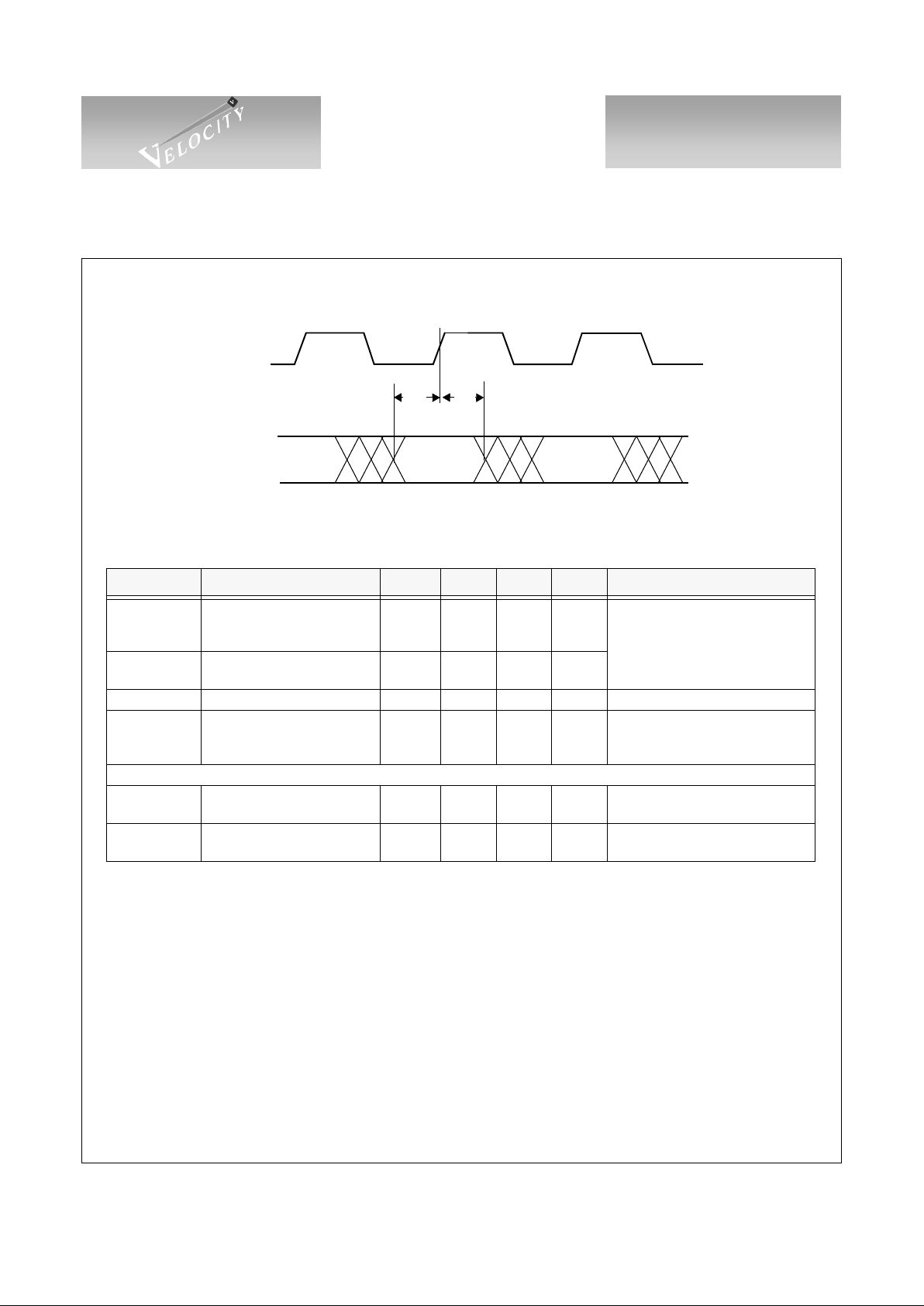
Figure 4: Transmit Timing Waveforms
Table 2: Transmit AC Characteristics
Parameters Description Min Typ Max Units Conditions
T
1
T(0:9) Setup time to the
rising edge of REFCLK
1.5 ——ns
Measured between the valid data
level of T(0:9) to the 1.4V point o f
REFCLK
T
2
T(0:9) hold time after the
rising edge of REFCLK
1.0 ——ns
T
SDR,TSDF
TX+/TX- rise and fall time ——300 ps 20% to 80%, 50Ω load to VDD- 2.0
T
LAT
Latency from rising edge of
REFCLK to T0 appearing on
TX+/TX-
8bc —
8bc+
4ns
ns
bc = bit clocks
ns = nano second
Transmitter Output Jitter Allo catio n
RJ Random jitter (RMS) — 58ps
Measured at SO+/-, 1 sigma
deviation of 50% crossing point.
DJ
Serial data output
deterministic jitter (pk-pk)
— 30 80 ps
IEEE 802.3Z Clause 38.68 , t ested
on a sample basis
Data Valid
T(0:9)
T
1
T
2
REFCLK
Data Valid
Data Valid
 Loading...