

VITESSE VSC7121QM Datasheet
VITESSE SEMICONDUCTOR CORPORATION
Page 1
8/31/98
741 Calle Plano, Camarillo, CA 93012 • 805/388-3700 • FAX: 805/987-5896
VITESSE
SEMICONDUCTOR CORPORATION
Data Sheet
SC7121
Quad Port Bypass Circuit for 1.0625 Gbit/sec
Fibre Channel Arbitrated Loop Disk Arrays
G52110-0, Rev. 4.1
Description
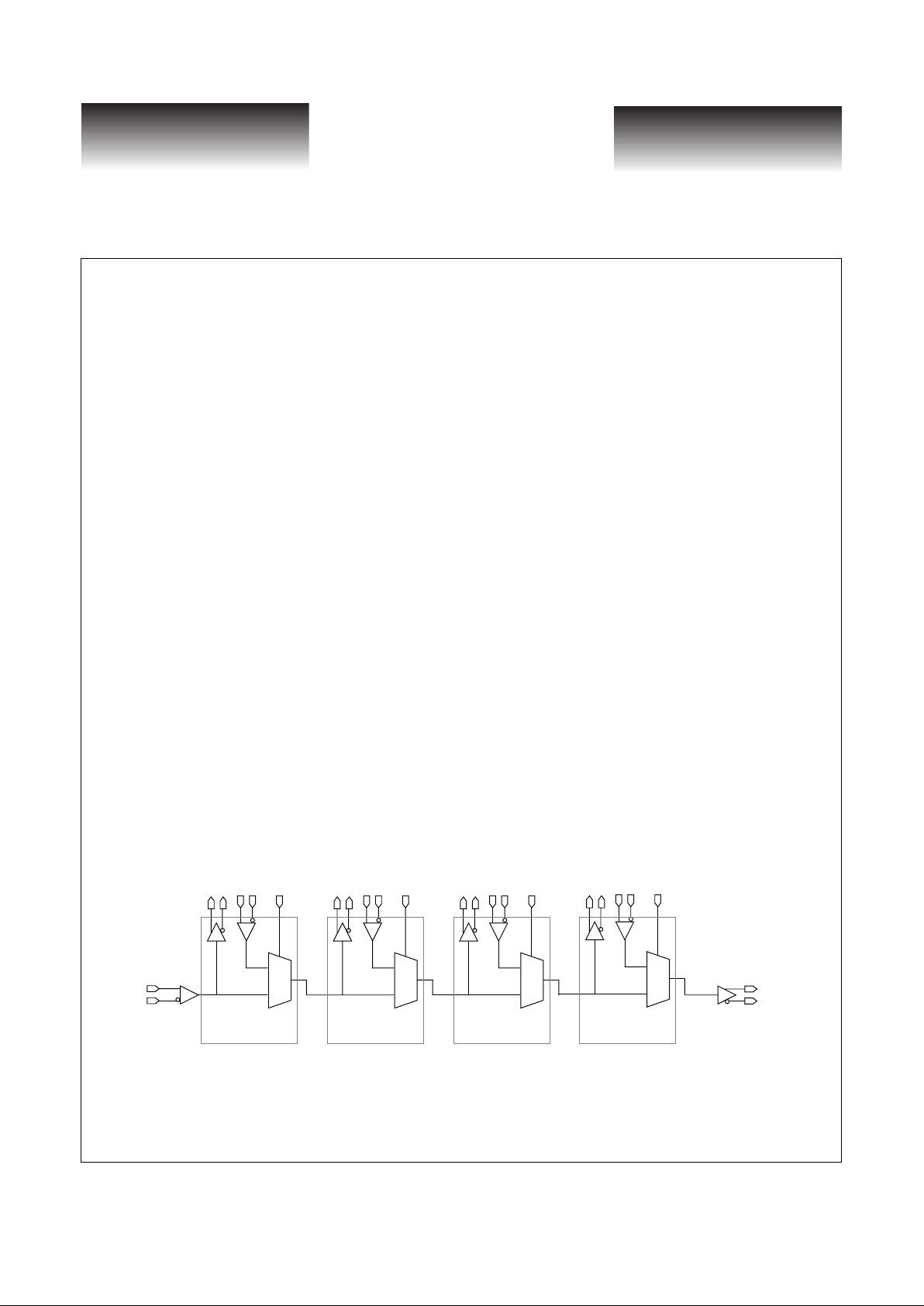
The VSC7121 is a Quad Port Bypass Circuit (PBC). Four Fibre Channel PBC’s are cascaded into a single
part to minimize part count, cost, high frequency routing, and jitter accumulation. Port Bypass Circuits are used
to provide resiliency in Fibre Channel Arbitrated Loop (FC-AL) architectures. PBC’s are used within FC-AL
disk arrays to allow for resiliency and hot swapping of FC-AL drives.
A Port Bypass Circuit is a 2:1 Multiplexer with two modes of operation: NORMAL and BYPASS. In NORMAL mode, the disk drive is connected to the loop. Data goes from the 7121’s L_SOn pin to the Disk Drive RX
input and data from the disk drive TX output goes to the 7121’s L_SIn pin. Refer to Figure 2 for disk drive
application. In BYPASS mode, the disk drive is either absent or non-functional and data bypasses to the next
available disk drive. Normal mode is enabled with a HIGH on the SEL pin and BYPASS mode is enabled by a
LOW on the SEL pin. Direct Attach Fibre Channel Disk Drives have an “LRC Interlock” signal defined to control the SEL function.
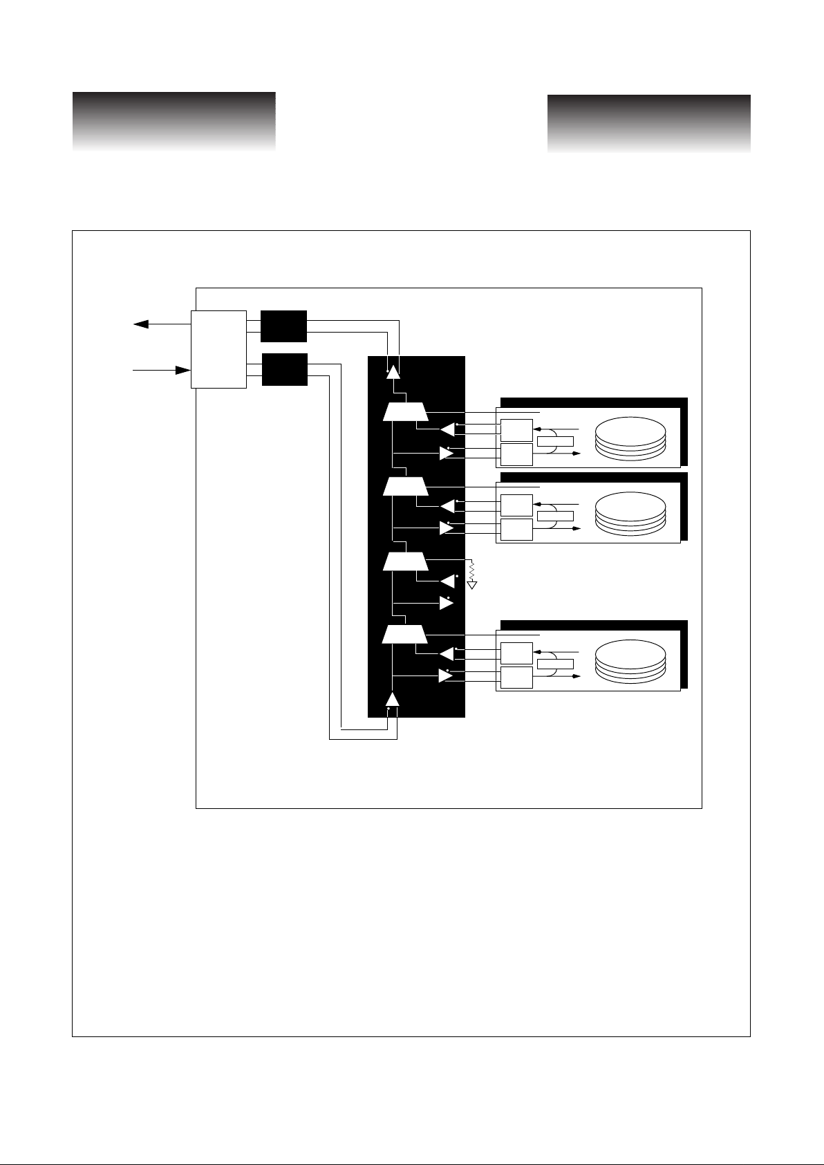
Using a VSC7121 in a single loop of a disk array is illustrated in Figure 2: “Disk Array Application”. FCAL drives are all expected to be dual loop. The VSC7121 is cascaded in a manner such that all the 7121’s internal PBC’s are used in the same loop. For dual loop implementations, two or more VSC7121’s should be used.
Allocating each VSC7121 to only one of two loops preserves redundancy, prevents a single point of failure and
lends itself to on-line maintainability.
7121 Block Diagram
The VSC7121 can be cascaded through the IN and OUT pins for arrays of disk drives greater than 4. For
disk arrays with a noninteger multiple of 4 disk drives, the unused PBC’s can be hardwired to bypass with a
external pulldown resistor.
• Supports ANSI X3T11 1.0625 Gbit/sec
FC-AL Disk Attach for Resiliency
• Fully Differential for Minimum
Jitter Accumulation.
• Quad PBC’s in Single Package
• TTL Bypass Select
• High Speed, PECL I/O’s Referenced to V
DD
.
• 0.5W Typical Power Dissipation
• 3.3V Power Supply
• 44-Pin, 10mm PQFP
LSI1+
LSI1-
LSO1+
LSO1-
IN+
IN-
OUT+
OUT-
SEL1
LSI2+
LSI2-
LSO2+
LSO2-
SEL2
LSI3+
LSI3-
LSO3+
LSO3-
SEL3
LSI4+
LSI4-
LSO4+
LSO4-
SEL4
1
00
1
0
1
0
1
PBC1
PBC2 PBC3 PBC4
VITESSE
SEMICONDUCTOR CORPORATION
Data Sheet
VSC7121
Quad Port Bypass Circuit for 1.0625 Gbit/sec
Fibre Channel Arbitrated Loop Disk Arrays
Page 2
VITESSE SEMICONDUCTOR CORPORATION
741 Calle Plano, Camarillo, CA 93012 • 805/388-3700 • FAX: 805/987-5896
8/31/98
G52110-0, Rev. 4.1
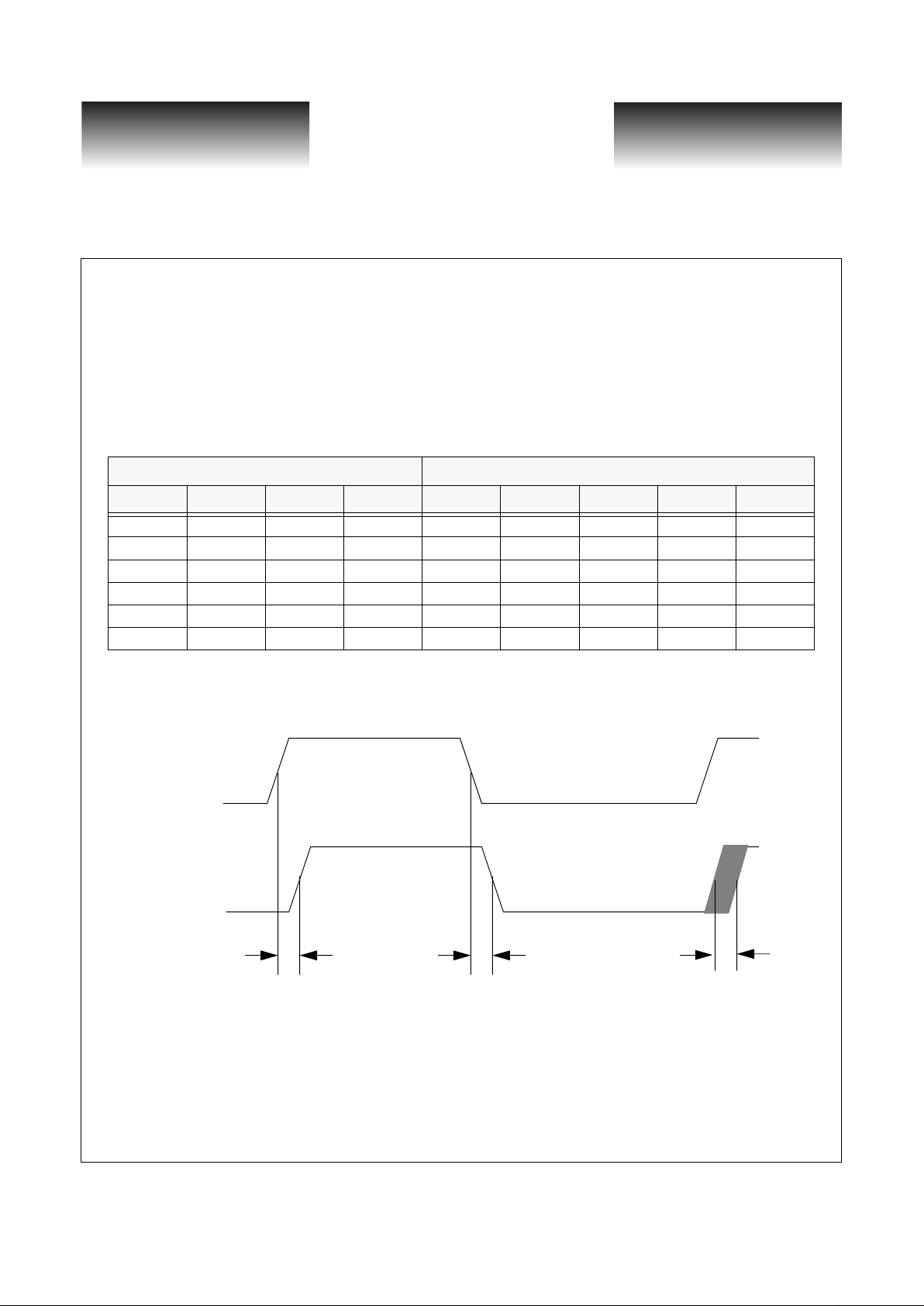
T able 1 is a truth table detailing the data flow through the VSC7121. Figure 1 shows a timing diagram of the
data relationship in the VSC7121. There are no critical timing (setup, hold, or delay) parameters for the
VSC7121 as this part routes the serial data encoded with the baud clock that is extracted by a Fibre Channel
receiver. The primary AC parameter of importance is the jitter or data eye degradation inserted by the port
bypass circuit. The design of the VSC7121 minimizes jitter accumulation by using fully differential circuits.
This provides for symmetric rise and fall delays as well as noise rejection.
Table 1: Truth Table
Figure 1: Timing Waveforms
SELECT STATE
DATA OUTPUTS
SEL1 SEL2 SEL3 SEL4 OUT SO4 SO3 SO2 SO1
LLLLININININ
IN
L L L H SI4 IN IN IN
IN
L L H L SI3 SI3 IN IN
IN
L H L L SI2 SI2 SI2 IN
IN
H L L L SI1 SI1 SI1 SI1
IN
HHHHSI4SI3SI2SI1
IN
T
1
T
2
T
jitter
OUT+/LSO1+/LSO2+/LSO3+/LSO4+/-
IN+/-
LSI1+/-
LSI2+/-
LSI3+/-
LSI4+/-
VITESSE SEMICONDUCTOR CORPORATION
Page 3
8/31/98
741 Calle Plano, Camarillo, CA 93012 • 805/388-3700 • FAX: 805/987-5896
VITESSE
SEMICONDUCTOR CORPORATION
Data Sheet
SC7121
Quad Port Bypass Circuit for 1.0625 Gbit/sec
Fibre Channel Arbitrated Loop Disk Arrays
G52110-0, Rev. 4.1
Figure 2: Disk Array Application
0
1
0
1
0
1
0
1
RX
TX
E_STORE
LRC Interlock
FC-AL DISK DRIVE
RX
TX
E_STORE
LRC Interlock
FC-AL DISK DRIVE
VSC7121 QUAD PORT BYPASS CIRCUIT
RX
TX
E_STORE
LRC Interlock
FC-AL DISK DRIVE
Pulldown for Bypass
in Absense of Disk Drive
7120
7120
Optics
or
Copper
JBOD
normal
normal
normal
bypass
Dual SC
or
DB-9
7120
7120
VITESSE
SEMICONDUCTOR CORPORATION
Data Sheet
VSC7121
Quad Port Bypass Circuit for 1.0625 Gbit/sec
Fibre Channel Arbitrated Loop Disk Arrays
Page 4
VITESSE SEMICONDUCTOR CORPORATION
741 Calle Plano, Camarillo, CA 93012 • 805/388-3700 • FAX: 805/987-5896
8/31/98
G52110-0, Rev. 4.1
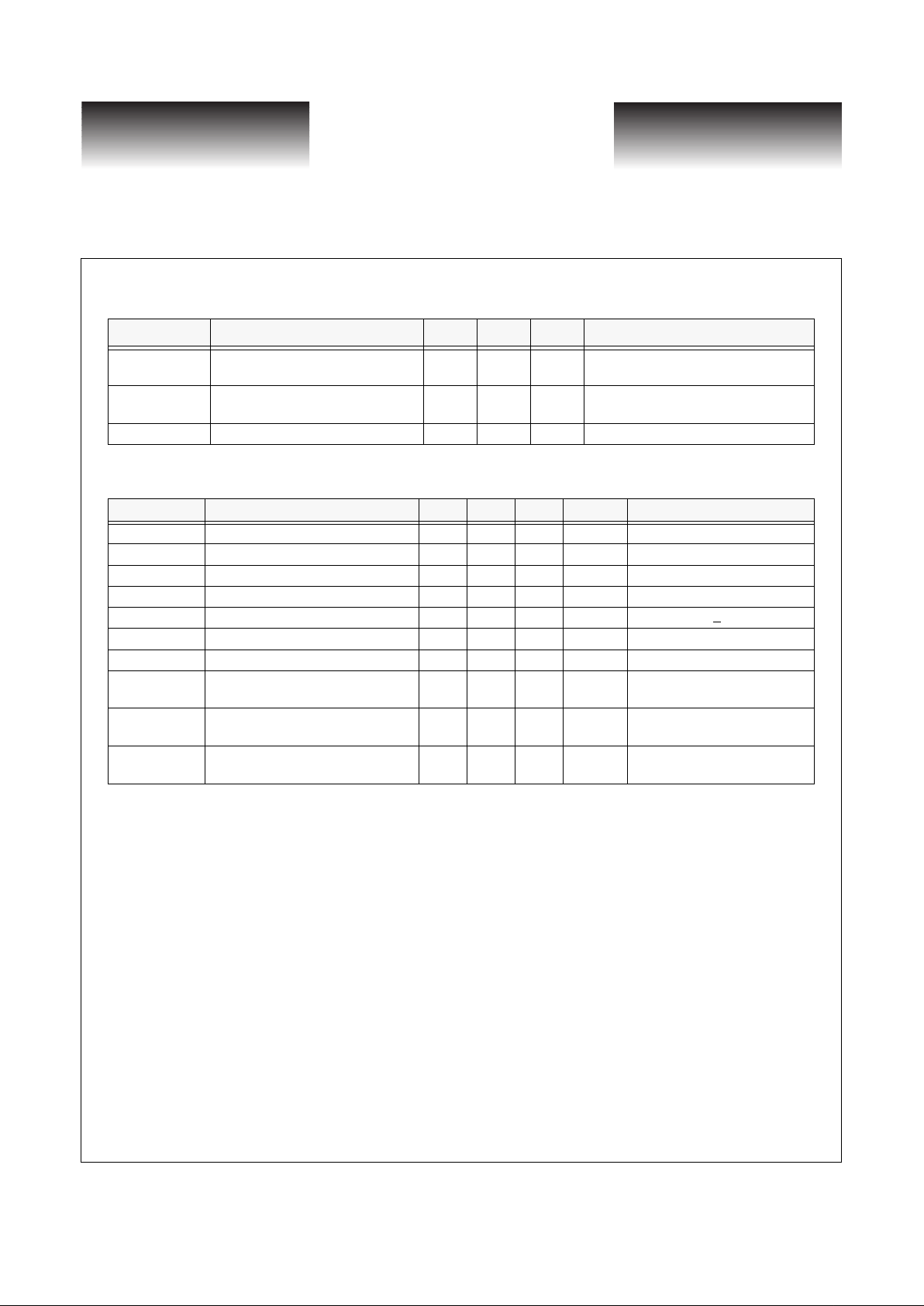
Table 2: AC Characteristics
(Over recommended operating conditions).
Table 3: DC Characteristics
(Over recommended operating conditions).
Parameters
Description Min. Max. Units Conditions
T
1
Flow-Through Propagation Delay
Rising Edge to Rising Edge
7.0 ns
Delay with all circuits bypassed. 75
Ohm Load
T
2
Flow through Propagation Delay
Falling Edge to Falling Edge
7.0 ns
Delay with all circuits bypassed. 75
Ohm load.
T
SDR
, T
SDF
Serial data rise and fall time — 300 ps. 20% to 80%, tested on a sample basis
Parameters
Description Min Typ Max Units Conditions
V
IH(TTL)
Input HIGH voltage (SEL - TTL) 2.0 — 5.5 V I
IH
< 6.6 mA @ V
IH
= 5.5 V
V
IL(TTL)
Input LOW voltage (SEL - TTL) 0 — 0.8 V —
I
IH(TTL)
Input HIGH current (SEL- TTL) — 50 500
µ
AV
IN
= 2.4 V
I
IL(TTL)
Input LOW current (SEL - TTL) — — -500
µ
AV
IN
= 0.5 V
V
DD
Supply voltage 3.10 — 3.50 V V
DD
= 3.30V +
5%
I
DD
Supply current — — 170 mA Outputs open, V
DD
= V
DD
max
P
D
Power Dissipation 0.6 W Outputs open, V
DD
= V
DD
max
∆
V
IN(DF)
Receiver differential peak-to-peak
Input Sensitivity, IN+/- & L_SIn+/-
300 2600 mVp-p
AC Coupled.
Internally biased at V
DD
/2 ∆
V
OUT(L_SO)
L_SOn+/- output differential peakto-peak voltage swing
1000 — 2200 mVp-p 50 Ω to V
DD
– 2.0 V
∆
V
OUT(OUT)
OUT+/- output differential peak-topeak voltage swing
1200 2200 mVp-p 50 Ω to V
DD
– 2.0 V
 Loading...