

VITESSE VSC6511RC Datasheet
VITESSE
A
V
SEMICONDUCTOR CORPORATION
dvance Product Information
SC6511
SMPTE-292M Serializer, Deserializer, and
Deserializer/Reclocker at 1.485Gb/s
Features
• Compliant with SMPTE-292M @ 1.485Gb/s
• Multiple Functions: Serializer, Deserializer,
and Deserializer with Reclocker
• 20 Bit TTL Interface @ 74.25 MHz
• Scrambler / Descrambler with ENABLE
• CRC Generator/Checker with ENABLE
• Data Framer aligns data and provides TRS on
SAV/EAV events
• Clock Multiplier and Recovery Units
• 2 or 4 configurable 75ohm cable driver o/ps
• 3.3V , Low power -- 700-1500mW typical
• 64-pin, 10x10x1.0mm Exposed Pad TQFP
General Description
The VSC6511 multi function SMPTE-292M compatible IC with Serializer, Deserializeror, or Deserializer
with reclocker modes which operate at 1.485Gb/s. As a Serializer, 20-bits of data (D19:0) are latched into the
part on the rising edge of REFCLK the n scrambled and serialize d out SDO0/SDO 0
optional CRC Generator may be enabled. As a Deserializer, serial data on SDI/SDI
and deserialized onto D[19:0]. Frame align ment on SAV/EAV, line detection and frame dete ction outputs are
provided. As a Deserializer with reclocker, the device functions as ain the deserializer mode above and serial
data on SDI/SDI
is recovered and retransmitted on SDO0/SDO0 and/or SDO1/SDO1.
and/or SDO1/SDO1. An
is recovered, de-scrambled
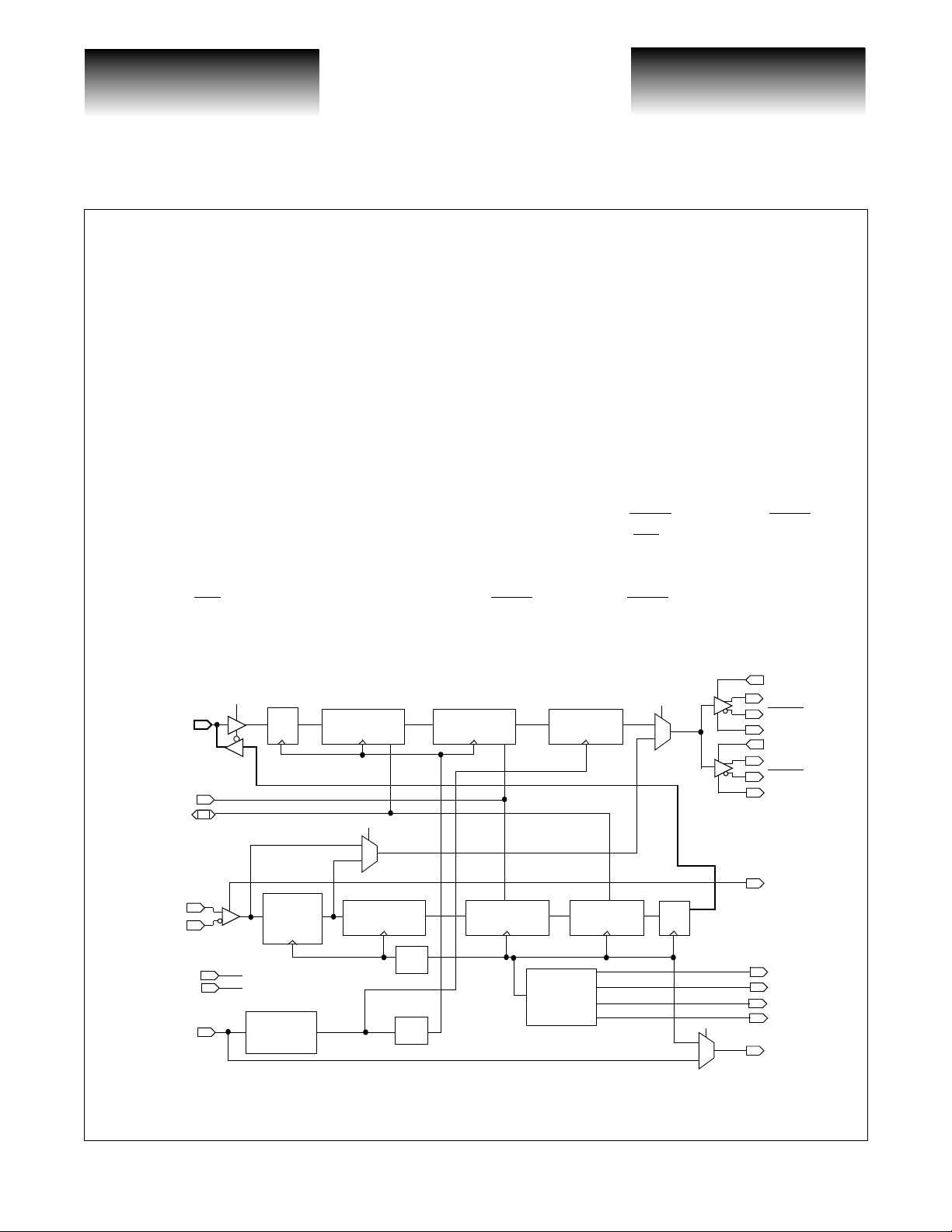
VSC6511 Block Diagram
OE0
SDO0
Draft Copy
D[19:0]
SCREN
CRC
IP
IN
MODE0
MODE1
REFCLK
74.25 MHz
D Q
Clock/
Recovery
Unit
Clock
Multiply
x20
CRC Gen
1.485 GHz
1.485 GHz
/20
/20
NRZI Decoder
Descrambler
SerializerScrambler
Framer
CABLE DRIVER
CRC CheckDeserializer
D Q
SDO0
ISET0
OE1
SDO1
SDO1
ISET1
OUTPUTS
SIGDET
1001
LINE
FRAME
HANC
RCLK
G52311-0, Rev. 2.0
4/10/00 741 Calle Plano, Camarillo, CA 93012 • 805/388-3700 • FAX: 805/987-5896
VITESSE SEMICONDUCTOR CORPORATION
Page 1

VITESSE
SEMICONDUCTOR CORPORATION
SMPTE-292M Serializer, Deserializer, and
Deserializer/Reclocker at 1.485Gb/s
Functional Description
The VSC6511 is a multifunction SMPTE-292M device which can be configured for different modes of
operation: Serializer , Deseri alizer, or Deserializer/Reclocker. Only one mode is available at a time. A discussion
of the individual building blocks of the device will be followed with specific configurations.
Clock Multiplier Unit (CMU)
The CMU generates the internal 1.485 GHz baud rate clock from the 74.25 MHz TTL REFCLK input. The
rising edges of the REFCLK are used by a PLL which multiplies the frequency by a factor of 20. This internal
baud rate clock is used by the Serializer, D eserializer and Reclocker. An off-chip 0.1uF capacitor sets the loop
bandwidth of the CMU. REFCLK should be a high quali ty, low jitter signal with sharp rise times in order to
minimize the amount of jitter transferred from the REFCLK through the CMU to the serializer. This optimizes
the signal quality at the output of the serializer.
A secondary function of the CMU is to divide the baud rate clock by 20 to produce an internal 74.25 MHz
clock which is frequency locked and phase aligned to REFCLK. This internal clock is used to latch the 20-bit
data bus D[19:0] into the input r egister o f the Serializer.
REFCLK is also buffered onto the RCLK output when in Serializer or Reclocker mode. This allows multiple devices to be daisy-chained in order to simplify REFCLK distribution to an array of devices.
CRC Generator
The twenty bits of transmit data from the input register is fed into a CRC Generator which calculates the
CRC and substitutes the value into the proper location within the video line. The CRC polynomial is CRC(X)=
18
+ X5 + X4 + 1). A controller monitors SAV/EAV position and uses this to control the CRC generator and
(X
insertion of the CRC result into the line. The CRC Generator is enabled only in Serializer Mode when CRC is
Draft Copy
HIGH. In other modes, or if CRC is LOW, the CRC Generator is disabled and powered down. CRC is a bidirectional pin.
Advance Product Information
VSC6511
Scrambler and NRZI Encoder
The twenty bits out of the CRC Generator are sent to the parallel Scrambler where the data is scrambled and
NRZI encoded using the combined generator polynomial of G(x)=(x
only when in Serializer Mode if SCREN is HIGH. Scrambling is disabled when SCREN is LOW and in other
modes.
Serializer
The data from the Scrambler is converted from 20-bits at 74.25 Mb/s t o 1 bit at 1.4 85 Gb/ s b y the S eria lizer
with D0 being transmitted first. Two differential PECL-style serial outputs are provided for transporting the
1.485 Gb/s signal. These out puts SDO0/ SDO0
izer mode) or the CRU of the Reclocker (in Deserializer/Reclocker mode). Each output, SDO0 and SDO1,
have independent TTL inputs, OE0 and OE1, which when HIGH enabl e the outputs and when LO W disab le t he
outputs. When disabled, the output buffer will be powered down and both legs will float HIGH.
Each output is compliant with the SMPTE-292M cable driver specification when driving 75 ohm loads. In
this application, a TBD ohm resistor should be connected from the ISET0/ISET1 pin to ground in order to control the current in the differential output amplifier. By low ering the ISET resistor, higher output swings may be
realized.
Page 2
741 Calle Plano, Camarillo, CA 93012 • 805/388-3700 • FAX: 805/987-5896 4/10/00
VITESSE SEMICONDUCTOR CORPORATION
and SDO1/SDO1 are supplied data fro m th e seriali zer (i n S eria l-
9
+ x4 +1)(x+1). Scrambling is enabled
G52311-0, Rev 2.0
VITESSE
A
V
SEMICONDUCTOR CORPORATION
dvance Product Information
SC6511
Serial Input
The differential PECL-style input, SDI/SDI, is the input source for 1.485 Gb/s SMPTE-292M data in the
Deserializer and Reclocker modes. This input is ignored in Serializer mode.
Clock Recovery Unit
The serial data on the SDI/SDI inpu t is sent to the digital Clock Re covery Unit (CRU) which extracts the
clock and retimes the data. This digital CRU is completely m onolithic an d requires no external comp onents.
Furthermore, it automatically l ocks onto d ata when p resent and lo cks to REFCLK when data i s not presen t. This
eliminates the need for the system to control the CRU. The CRU is enabled only in the Deserializer and Deserializer/Reclocker modes.
Deserializer
The reclocked serial bit stream is deserialized into a 20-bit parallel charact er. D0 is serially receiv ed prio r to
D1. The VSC6511 provides a TTL recovered clock, RCLK at one t went ieth of t he serial b aud rate. This clock is
generated by dividing down the high-speed clock from the CRU which is phase locked to the serial data. The
deserializer is enabled only in the Deserializer and Deserializer/Reclocker modes.
If serial input data is not present, or do es not m eet the required baud rate, the VSC6511 will continue to
produce a recovered clock so that downstream logic may continue to function. The RCLK output frequency
under these circumstances will differ from their expected frequency by less than +
SMPTE-292M Serializer, Deserializer, and
Deserializer/Reclocker at 1.485Gb/s
1%.
Descrambler and NRZI Decoder
The VSC7152 contains a descrambler/NRZI Decoder wh ich processes the r ecovered serial data and outputs unscrambled and NRZI decod ed serial data from th e deserializ er. The serial scrambled data is descrambled/
NRZI decoded assuming data has been scrambled/NRZI encoded with the following combined generator poly-
Draft Copy
nomial: G(x)=(x
LOW. The descrambler is enabled only in the Deserializer mode.
CRC Checker
The 20-bit data from the Descrambler is sent to the CRC Checker where a running CRC checksum is continuously calculated. As 20-bit data is sent out of the chip, the CRC output pin is asserted if the checksum did
not meet the val ue expect ed. This error is asse rted from the f i rst CRC Error until the end of the li ne. A controll er
monitors the 20-bit da ta out of the se rializer for S AV/EAV frames in order to control t he CRC Checker. The
CRC Checker is enabled only in Deserializer and Deserializer/Reclocker modes.
Frame Aligner
The VSC6511 monitors the serial data stream for SAV/EAV characters. These characters should be located
within each line of video data. If SAV/EAV is not det ected wi th in t he pe riod of one line, the Framer sends a signal to the Deserializer to shift the data o ne bit. The Fram er then lo oks for SAV/EAV and the process repea ts
until properly detected. Without these patterns, serial data is not aligned in any way with the parallel outputs.
The Framer outputs a once-per-li ne (LINE) , Horizo nt al ANCill iary period (HANC), 1.001/ 1. 000 ou tpu t (1.0 01)
and a once-per-frame (FRAME) signal indicating the detection of the proper synchronization pulse in the data.
Framing is enabled only in Deserializer mode.
The Frame Aligner also outputs the L INE, FR AME an d HANC output s si gnals . Th e ti mi ng of t hese si gnals
is indicated below.
9+x4
+1)(x+1). Descram bling is en abled with t he SCREN input is HI GH and di sabled w hen
G52311-0, Rev. 2.0
4/10/00 741 Calle Plano, Camarillo, CA 93012 • 805/388-3700 • FAX: 805/987-5896
VITESSE SEMICONDUCTOR CORPORATION
Page 3
VITESSE
SEMICONDUCTOR CORPORATION
SMPTE-292M Serializer, Deserializer, and
Deserializer/Reclocker at 1.485Gb/s
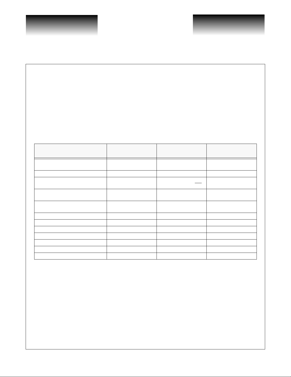
Table 1: Frame Aligner Output Timing
D10-19 D0-9 LINE FRAME HANC CRCERR
DATA DAT A 0 0 0 0
--- --- 0 0 0 0
VIDEO
ACTIVE
EAV
LINE
CRC
HORIZ
BLANK
SAV
Draft Copy
VIDEO
ACTIVE
DATA DAT A 0 0 0 0
3FF3FF0000
0000000000
0000000000
XYZ XYZ 0 0 0 0
LN0LN00000
LN1LN111*0 0
CRC0 CRC0 0 0 0 0
CRC1 CRC1 0 0 0 0 or 1
DATA DAT A 0 0 1 0
--- --- 0 0 1 0
DATA DAT A 0 0 1 0
3FF3FF0000
0000000000
0000000000
XYZ XYZ 0 0 0 0
DATA DAT A 0 0 0 0
DATA DAT A 0 0 0 0
--- --- 0 0 0 0
* FRAME is HIGH only if LN0/LN1 indicates the first line of a frame.
** CRCERR is HIGH only during CRC1 if the CRC is incorrect.
Advance Product Information
VSC6511
D[19:0] Databus
As mentioned previously, in Serializer mode D[19:0] is configured as a input. In Deserializer mode,
D[19:0] is configured as an output.
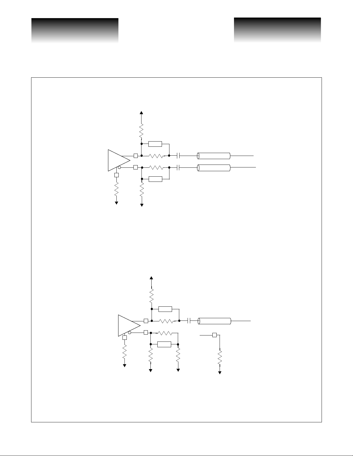
Application Information
The VSC6511 cable driver output is intended to fully comply with the SMPTE-292M cable driver specifications. This includes an 800mV swing and a return loss of more than 15dB. The circuit shown below shows
how to connect the output of the VSC6511 to the 75 ohm ca ble and downstream device. The output of the
VSC6511 is actually 120 0mV. The ou tput termination circuit shown below attenuates the ou tput signal to
800mV and ensures a return loss better than -15dB. The ISET resistor is 1 .78K
Page 4
741 Calle Plano, Camarillo, CA 93012 • 805/388-3700 • FAX: 805/987-5896 4/10/00
VITESSE SEMICONDUCTOR CORPORATION
G52311-0, Rev 2.0
VITESSE
A
V
SEMICONDUCTOR CORPORATION
dvance Product Information
SC6511
Figure 1: High Speed Interconnect Example (Differential)
6511
1.78K
ISETx
V
SS
SMPTE-292M Serializer, Deserializer, and
Deserializer/Reclocker at 1.485Gb/s
V
DD
75
10nH
75
75 ohm Cables
75
10nH
75
V
DD
NOTE: All resistors are 1%
WARNING: SUBJECT TO CHANGE
Figure 2: High Speed Interconnect Example (Single Ended)
Draft Copy
6511
1.78K
ISETx
V
SS
NOTE: All resistors are 1%
Optional use of external Voltage Reference provides tighter swing tolerance
V
DD
75
10nH
75
75 ohm Coax
75
10nH
75
V
DD
75
V
DD
or
37.5
V
DD
G52311-0, Rev. 2.0
4/10/00 741 Calle Plano, Camarillo, CA 93012 • 805/388-3700 • FAX: 805/987-5896
VITESSE SEMICONDUCTOR CORPORATION
Page 5
VITESSE
SEMICONDUCTOR CORPORATION
SMPTE-292M Serializer, Deserializer, and
Deserializer/Reclocker at 1.485Gb/s
The output swing of the VSC6511 is controlled through the ISETx pins and a VREF input. By connecting
an 1.78K ohm resistor, 1%, between VSS and ISETx the output swing will be controlled to within 800mV +/7%. An optional bandpass v ol tage refer ence may be used to furth er tigh ten t he out put swings by accurately driving the VREF input.
Configuration Modes:
The MODE(1:0) inputs configure the VSC6511 into its different modes of operation. The table below summarizes the different signals and circuits in the VSC6511 that change function in the different modes.
Table 2: Mode Configuration Features: Serializer Mode
SIGNAL/CIRCUIT
MODE1
MODE0
D[19:0] Data Bus 20-BIT OUTPUT 20-BIT OUTPUT 20-BIT INPUT
SDO0/SDO1 Serial Outputs NOT USED, DISABLED
RCLK Output
CRU Bypass Mux NOT ACTIVE
SDI Serial Input ACTIVE ACTIVE IGNORED
Draft Copy
CRC CRC is an error output CRC is an error output Enables CRC Generator
SIGDET Output ACTIVE AC TIVE DISABLED LOW
1.001 Output ACTIVE ACTIVE DISABLED LOW
FRAME Output ACTIVE ACTIVE DISABLED LOW
LINE Output ACTIVE ACTIVE DISABLED LOW
HANC Output ACTIVE ACTIVE DIS ABLED LOW
RECOVERED CLOCK
DESERIALIZER
MODE
HIGH
HIGH
FROM CRU
Advance Product Information
VSC6511
DESERIALIZER/
RECLOCKER MODE
LOW
HIGH
SOURCE IS CRU
OUTPUT OR SDI/SDI
RECOVERED CLOCK
FROM CRU
CRU OUTPUT GOES
TO SDO0/SDO1
SERIALIZER
MODE
LOW
LOW
SOURCE IS
SERIALIZER
BUFFERED REFCLK
CRU NOT ACTIVE
Page 6
741 Calle Plano, Camarillo, CA 93012 • 805/388-3700 • FAX: 805/987-5896 4/10/00
VITESSE SEMICONDUCTOR CORPORATION
G52311-0, Rev 2.0
VITESSE
A
V
SEMICONDUCTOR CORPORATION
dvance Product Information
SC6511
SMPTE-292M Serializer, Deserializer, and
Deserializer/Reclocker at 1.485Gb/s
Features: Serializer Mode
1. 20 Bit TTL Interface @ 74.25 MHz
2. On-chip Clock Multiplier Unit
3. On-Chip Scrambler and NRZI Encoder with ENABLE
4. CRC Generator with ENABLE
5. 2 or 4 user configurable 75ohm cable driver outputs
6. Output Signal Detect indicators
7. Buffered REFCLK output for easy clock distribution
8. 700 mW Typical Power
Description
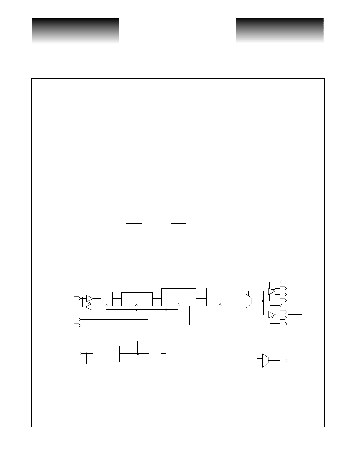
The VSC6511 can be configured as a 20-bit HDTV Serializer using the MODE[1:0] pins. A 74.25 MHz
TTL REFCLK is mul tiplied by 20 in the Clock M ultip lier Unit (C MU) to gene rate a 1. 485 GHz b it rate c lock.
The CMU aligns a divided- b y-20 clock wit h REFCLK in order to latc h the 20-bit TTL data b us D[19:0] into the
Input Register. When enabled by CRC being HIGH, the data is mo nito red for S AV/EAV and a CRC checksum i s
calculated and inserted into the data stream at the appropriate point in each video line. The data is then scrambled and NRZI encoded, only if this stage is enabled by SCREN=HIGH. The data is then serialized and output
on the differential outputs, SDO0/SDO0
driving specifications. The scrambler and NRZI encoder can be disabled by setting the TTL input, SCREN to
LOW. The SDO0/SDO0
larly, the SDO1/SDO1
output can be disabled and forced HIGH by setting the TTL input OE0 to LOW. Simi-
output can be disabled and forced HIGH by setting the TTL input OE1 to LOW.
and SDO1/SDO1, which are compliant with the SMPTE 292M cable
Figure 3: Serializer Mode
Draft Copy
OE0
SDO0
SD
ISET0
OE1
SDO1
SDO1
ISET1
OUTPUTS
O0
RCLK
D[19:0]
CRCEN
SCREN
REFCLK
74.25 MHz
D Q
Clock
Multiply
x20
CRC Gen
1.485 GHz
/20
Scrambler
NRZI Encoder
*
Serializer
CABLE DRIVER
G52311-0, Rev. 2.0
4/10/00 741 Calle Plano, Camarillo, CA 93012 • 805/388-3700 • FAX: 805/987-5896
VITESSE SEMICONDUCTOR CORPORATION
Page 7
 Loading...