

VITESSE VSC6501RC Datasheet
VITESSE SEMICONDUCTOR CORPORATION
Page 1
4/10/00 741 Calle Plano, Camarillo, CA 93012 • 805/388-3700 • FAX: 805/987-5896
VITESSE
SEMICONDUCTOR CORPORATION
A
dvance Product Information
VSC6501
and Cable Driver at 1.485 Gb/s
SMPTE-292M Reclocker
G52310-0, Rev. 2.0
Draft Copy
Features
General Description
The VSC6501 is a SMPTE-292M compatible Reclocker with 2 or 4 user configurablable 75 ohm Cable
Driver outputs which operate at 1.485Gb/s. HDTV serial data on the SDI/SDI
inputs is recovered and retrans-
mitted on the SDO0/SDO0
and SDO1/SDO1 outputs. The CRU portion of the reclocker may be bypassed for
operation with non-HDTV data rates. The VSC6501 can be used to build routing switchers and video distribution amplifiers.
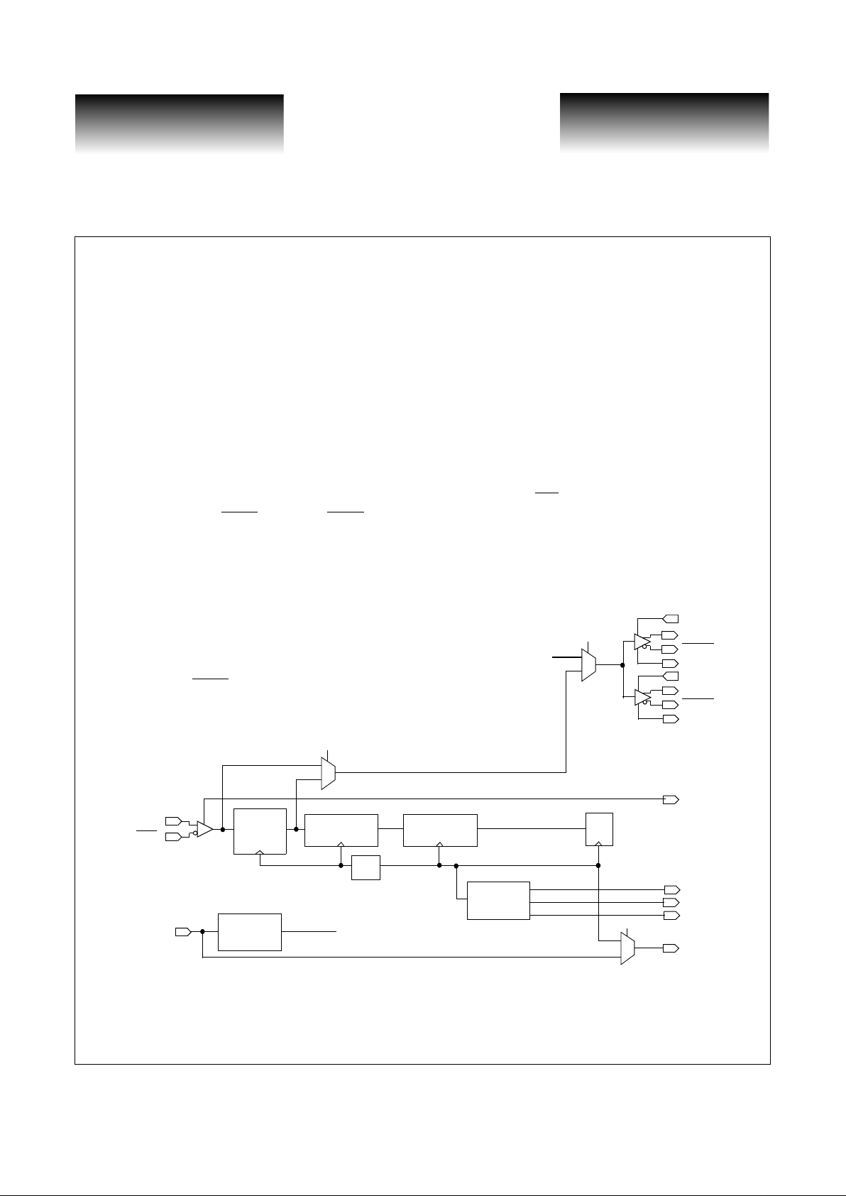
VSC6501 Reclocker Block Diagram
• Compliant with SMPTE-292M @ 1.485Gb/s
• Clock and Data Recovery
• 2 or 4 user Configurable 75 ohm cable driver
outputs
• CRU BYPASS mode for SMPTE 259M or
other data rates
• Buffered REFCLK output for distribution to
additional devices
• 3.3V, Low Power -- 800 mW typical
• 64-pin, 10x10x1.0mm Exposed Pad TQFP
LINE
FRAME
HANC
SDI
SDI
Clock/
Recovery
REFCLK
Clock
Multiply
1.485 GHz
74.25 MHz
x20
RCLK
1.485 GHz
BYP A SS
SDO0
SDO0
SIGDET
OE1
/20
ISET0
SDO1
SDO1
ISET1
Unit
*
CABLE DRIVER
OUTPUTS
DescramblerDeserializer
D Q
OE0
Framer
*

VITESSE
SEMICONDUCTOR CORPORATION
Advance Product Information
VSC6501
Cable Driver at 1.485 Gb/s
SMPTE-292M Reclocker and
Page 2
VITESSE
SEMICONDUCTOR CORPORATION
741 Calle Plano, Camarillo, CA 93012 • 805/388-3700 • FAX: 805/987-5896 4/10/00
G52310-0, Rev. 2.0
Draft Copy
Reclocker Functional Description
Clock Multiplier Unit (CMU)
The CMU generates the internal 1.485 GHz baud rate clock from the 74.25 MHz TTL REFCLK input. The
rising edges of the REFCLK are used by a PLL which multiplies the frequency by a factor of 20. An off-chip
0.1uF capacitor sets the loop bandwidth of the CMU. REFCLK should be a high quality, low jitter signal with
sharp rise times in order t o mini mi ze the amount of jitter tr ansf err ed f r om the REFCLK through the CMU to t he
serializer. Although not shown on the block diagram, the digital CRU requires the baud rate clock of the CMU
for proper operation.
REFCLK is also buffered onto the RCLK output allowing multiple devices to be daisy-chained in order to
simplify REFCLK distribution to an array of devices.
Serial Input
The differential PE CL-sty le i np ut , SDI/S DI, is t he i np ut source f or 1.485 Gb/s SMPTE 292M data. An analog signal detector monitors the input signal for valid amplitude and outputs status on the SIGDET pin. If SIGDET is HIGH, the differential input swing is greater than 400 mV. If SIGDET is LOW, the differential swing is
below 200 mV. If the input swing is between 200 and 400 mV, the SIGDET output is indeterminate. The SIGDET function is disabled in Serializer mode and will output a LOW.
Clock Recovery Unit
The serial data on the SDI /SDI inpu t is sent to the digital Clock Recovery Unit (CRU) which extracts the
clock and retimes the data. This dig ital CRU is completely monol ithic and re quires no external comp onents.
Furthermore, it automaticall y locks ont o dat a when present and lo cks to REFCLK when data i s not presen t. This
eliminates the need for the system to control the CRU.
Descrambler and NRZI Decoder
The VSC6501 contains a descrambler whic h processes the recovered serial data and outputs u nscrambled
serial data from the deserialize r. The serial scrambled data is descrambled/NRZ I decoded assu ming data ha s
NRZI encoded with the following combined generator polynomial: G(x)=(x
9+x4
+1)(x+1). Descrambling is
enabled with the SCREN input is HIGH and disabled when LOW.
Pattern Detector
The VSC6501 monitors the serial data stream for SAV/EAV characters. These characters should be located
within each line of video data. If SAV/EAV is not det ect ed wi th in t he p eriod of one l in e, th e Framer send s a signal to the Deserializer to shift the data one bit. The Frame then looks for SAV/EAV and the process repeats until
properly detected. Without these patterns, serial data is not aligned in a ny way with the parallel outputs. The
Framer outputs a once-per-line (LINE) and a once-per-frame (FRAME) signal indicating the detection of the
proper synchronization pulse in the data.
VITESSE SEMICONDUCTOR CORPORATION
Page 3
4/10/00 741 Calle Plano, Camarillo, CA 93012 • 805/388-3700 • FAX: 805/987-5896
VITESSE
SEMICONDUCTOR CORPORATION
A
dvance Product Information
VSC6501
and Cable Driver at 1.485 Gb/s
SMPTE-292M Reclocker
G52310-0, Rev. 2.0
Draft Copy
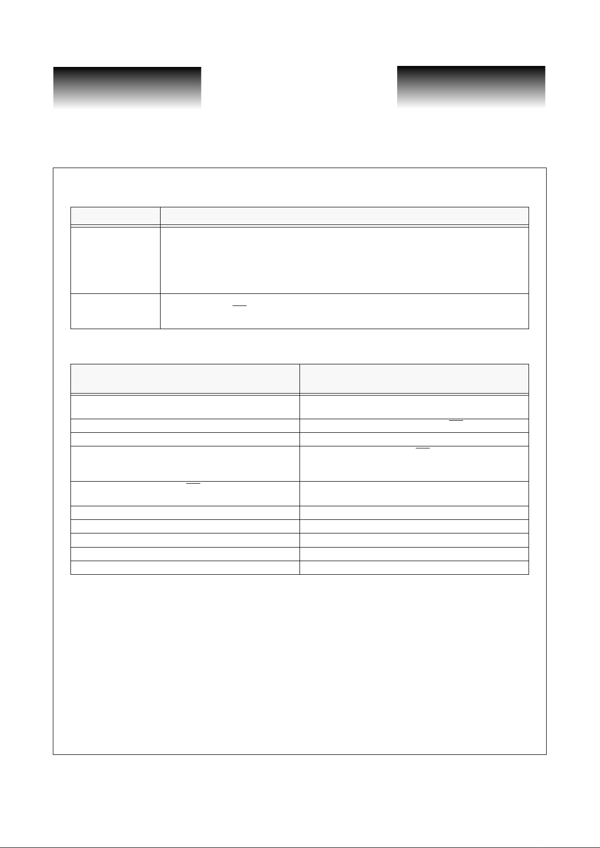
Table 1: Reclocker Logic Signals
Table 2: Reclocker Operation
Application Information
The VSC6501 cable dri v e r output is in te nded to full y compl y with the SMP TE 292M cab le driver specifications. This includes an 800mV swing and a return loss of less than -15dB. The circuit shown below shows how
to connect the output of the VSC6501to the 75 ohm cable and downstream device. The output of the VSC6501
is actually 1200mV. The output termination circuit show n below attenuates the output signal to 800mV and
ensures a return loss better than -15 dB. The ISET resistor is 1.78K
SIGNAL FUNCTION
292M
292M Output:
When HIGH, indicates that the output of the CRU is a SMPTE-292M style signal. This output
combines the analog signal detect with a state machine which monitors SAV/EAV events. If 4000
words occur without an SAV/EAV, then this output goes LOW to indicate invalid data. This output
goes HIGH if the analog signal detection is asserted and an SAV/EAV is located withi n t he l ast 4000
words.
BYPASS
BYPASS Input:
When HIGH, SDI/SDI
are routed around the CRU directly to the SDO0/SDO1 outputs. When LOW,
the output of the CRU is sent to SDO0/SD)1 outputs.
SIGNA L
RECLOCKER
Operation
292M
BYP AS S
Active
Active
O0/O1 Serial Outputs SOURCE IS CRU SDI/SDI
RCLK Output BUFFERED REFCLK
CRU Bypass Mux
SDI/SDI
GOES TO
SDO0/SDO1
SDI/SDI
Serial Input
ACTIVE
SIGDET Output ACTIVE
FRAME Output ACTIVE
1.001 Output ACTIVE
LINE Output ACTIVE
HANC Output ACTIVE
VITESSE
SEMICONDUCTOR CORPORATION
Advance Product Information
VSC6501
Cable Driver at 1.485 Gb/s
SMPTE-292M Reclocker and
Page 4
VITESSE
SEMICONDUCTOR CORPORATION
741 Calle Plano, Camarillo, CA 93012 • 805/388-3700 • FAX: 805/987-5896 4/10/00
G52310-0, Rev. 2.0
Draft Copy
Figure 1: High Speed Interconnect Example (Differential)
Figure 2: High Speed Interconnect Example (Single Ended)
6501
V
DD
75
75 ohm Cables
75
75
75
V
DD
1.78K
ISETx
NOTE: All resistors are 1%
10nH
10nH
V
SS
WARNING: SUBJECT TO CHANGE
6501
V
DD
75
75 ohm Coax
75
NOTE: All resistors are 1%
10nH
Optional use of external Voltage Reference provides tighter swing tolerance
1.78K
ISETx
V
SS
75
75
V
DD
10nH
75
V
DD
37.5
V
DD
or
 Loading...