

VITESSE
SEMICONDUCTOR CORPORATION
Preliminary Datasheet
SC6424
500 Mb/s Video
Shift Register IC
Features
• Multiplex or Demultiplex Operation
• Selectable Shift Register Length
• 500Mb/s Operation using internal timing
• 250Mb/s Operation using external timing
• Functional Replacement for Bt424
• External ECL Reference Voltage (-1.32 V)
• ECL and TTL I/Os: ECL for high-speed interface,
TTL for low-speed interface
• Power Supplies: +3.3V an d -2V @ 2.7 Watts (Max.)
o
• Commer cial (0
to +70oC) Temperature Range
• Package: 14mm x 20mm 128 PQFP
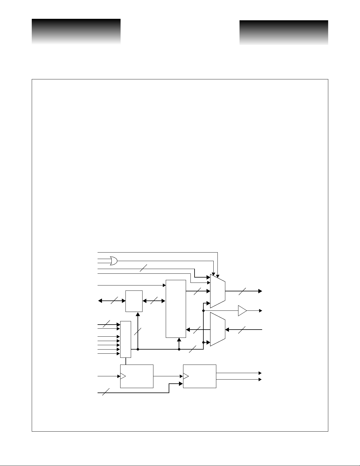
General Description
The VSC6424 is a 500Mb/s vide o shift register IC that is b ased on a 40-bit us er-configured shift register.
The shift register may b e used ei t her as a mult ip lexer (parallel in , serial out ) o r as a demul t iplexer (serial in, parallel out). The VSC642 4 can be configured int o 8 5 - bi t, 8 4- bi t , 5 8- b it , 4 10- bi t , 2 16 - bit , 2 20- bi t , 1 3 2- bi t, or 1
40-bit shift register.
VSC6424 Functional Block Diagram
OEN
HBLANK
Low
Speed
Interface
(TTL)
VBLANK
A<0:4>
AEN/RETIME
SIN
(ECL)
SB<0:39>
S<0:2>
MODE
INT/EXTN
OPS
LLDN
SEN/DIVC
SLDN/SYNC
CLK
(ECL)
SP<0:2>
40
3
3
Input
Latch
(TTL)
(TTL)
Timing Control
Clock
Generator
5
40
40-bit
Shift
Register
40
10
Phase
R o ta tio n
MUX
DEMUX
8
10
DOUT<0:7>
CLKOUT
DIN<0:9>
CLKE(ECL)
CLKT(TTL)
High
Speed
Interface
(ECL)
G52236-0, Rev 3.0
7/13/99 741 Calle Plano, Camarillo, CA 93012 • 805/388-3700 • FAX: 805/987-5896
VITESSE
SEMICONDUCTOR CORPORATION Page 1
VITESSE
SEMICONDUCTOR CORPORATION
00 Mb/s Video
hift Register IC
Preliminary Datash ee t
VSC6424
Functional Description
The VSC6424 is a 40-bit user configurable shift register designed to provide general purpose serialization
or de-serialization for high speed designs. The VSC6424 provides both multiplexer (MUX) and demultiplexer
(DEMUX) operations in a single package. With the ability to generate timing signals internally or have them
provided externally the VSC6424 maintains the highest design flexibility.
The low speed signals (parallel dat a, c onfiguration, external timing) use a TTL interface and t he high-speed
signals (serial data, high-speed clock) use an ECL interface. Two power supplies are utilized, +3.3 Volts and -2
Volts, dissipating a maximum of 2.7 Watts. A -1.32V external reference voltage is necessary for the ECL interface. The part is packaged in a 14mm x 20mm 128-pin plastic quad flat pack with an exposed heat spreader.
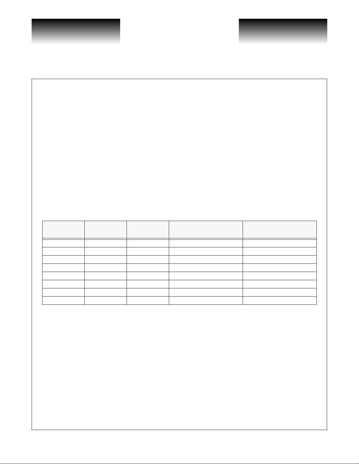
Shift Register Mode/Modulus Selection
The shift register can be setup to work as multipl exer or as a demultiplexer. The MODE pin controls the
direction of operation (MUX or DEMUX). The select pins S<0:2> put the shift register in one of 8 configurations shown in Table 1
Table 1: Modulus of Operation
S2 S1 S0
0 0 0 8 4:1 10 1:4
0 0 1 8 5:1 8 1:5
0 1 0 5 8:1 5 1:8
0 1 1 4 10:1 4 1:10
1 0 0 2 16:1 2 1:16
1 0 1 2 20:1 2 1:20
1 1 0 1 32:1 1 1:32
1 1 1 1 40:1 1 1:40
Multiplexer
MODE = 0
Demultiplexer
MODE = 1
Internal Timing
The VSC6424 can be set up to use either internal or external timing sources. The VSC6424 contains an
internal timing generato r that provides load an d output rate s dependin g on the modu lus selected for th e shift
register. The timing generator takes an external high speed differential clock (CLK). Internal timing mode must
be used for designs above 250MHz.
The internal timing generator also provides two low-speed clock outputs, CLKT(TTL) and CLKE(ECL).
The low speed clock is brought out so that other ICs can use th is to latch the low speed data while in DMUX
mode. The slow speed clock output can be the same as the internal clock, or 1/2 the internal frequency by setting DIVC high. These outputs can also be shifted in 45 degree increme nts, using the phase se lect pins
SP<0:2>, to allow compensation for trace delays on the board. Phase rotation is not available in divide by 5 or
divide by 10 mod es.
The internal high speed clock is also bro ught out to a differential ECL ou tput (CLKOUT). This output is
provided for clocking of the high speed data into the next IC.
Page 2
741 Calle Plano, Camarillo, CA 93012 • 805/388-3700 • FAX: 805/987-5896 7/13/99
VITESSE
SEMICONDUCTOR CORPORATION G52236-0, Rev 3.0
VITESSE
SEMICONDUCTOR CORPORATION
Preliminary Datasheet
SC6424
The Output Phase Shift (OPS) signal gives the capability of selecting which edge of the high speed clock
the DOUT data is synchron ized to . When OPS is low, DOUT comes out on the rising edge of CLK. When OPS
is high, DOUT comes out on the falling edge of CLK. The high speed output clock (CLKOUT) is not affected by
the state of OPS.
500 Mb/s Video
Shift Register IC
External Timing
To provide a functional replacement for older designs using the Bt424, former ly manufactured by BrookTree, the VSC6424 provides an external timing mode. This can be accomplished by setting the INT/EXTN pin
low to bypass the internal timing generator. In this case the load and shift timing signals are provided through
the Shift Enable(SEN ), Shift Register Load Control(SLDN), and the Latch Load C on trol(LLDN) pins.
The VSC6424 has two cycles of propaga tion del ay in mul ti plexer mode where t he Bt 424 onl y has o ne. Thi s
provides the ability to control on which edge of the output clock the output data is clocked on. With the Output
Phase Select (OPS) pin low the output data (DOUT) is synchronous with the positive edge of CLKOUT, where
if OPS is high the output data is synchronous to the negative edge of CLKOUT. See Figure 6 for a timing diagram example with OPS low.
The shift register can also be lo aded with seri al dat a while in e xternal t iming mode. T his is accompl ished b y
inputting data into the shift register through the Serial Input (SIN) pin. The data is latched on the rising edge of
the CLK while SLDN is high and SEN is low. The data is then shifted to the output pins on each clock cycle
once Shift Enable (SE N ) is set high.
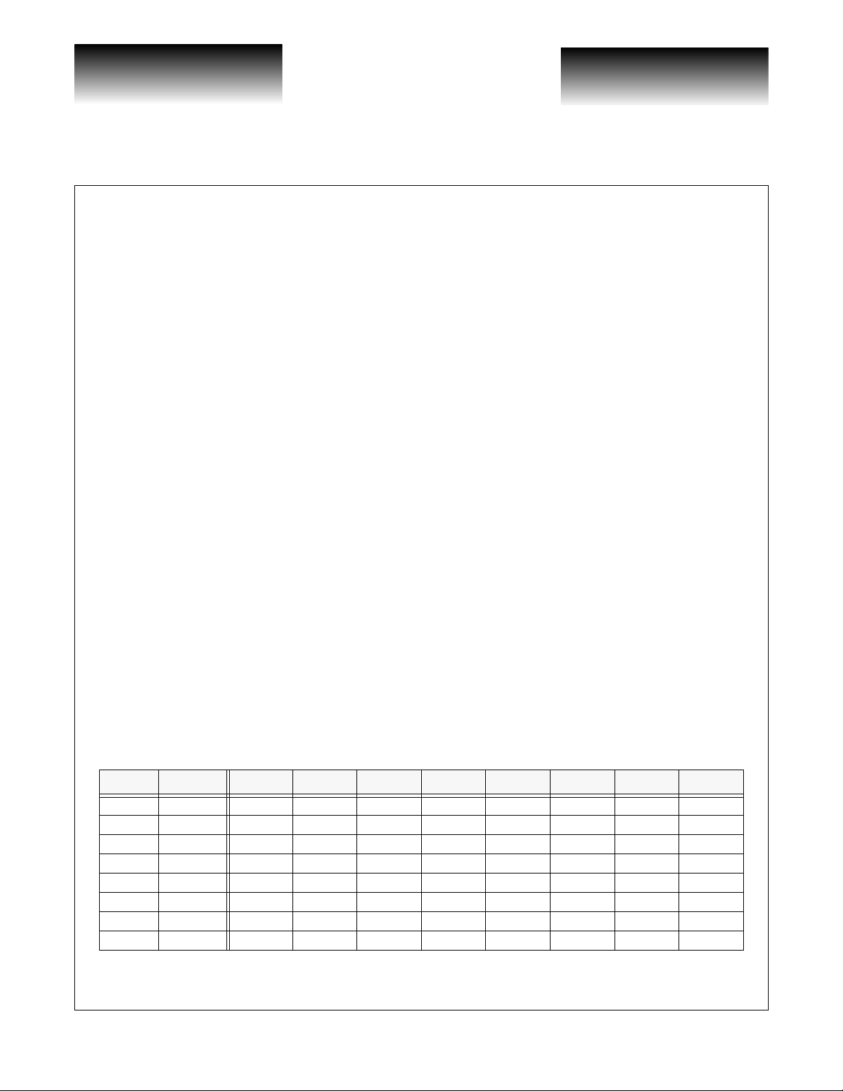
I/O Mapping
There are 10 high speed ECL data inputs and 8 high speed ECL data outputs. Some configurations of operation do not use all these inputs and outputs. T he sta te of t he out put s n ot being used in a giv en mode is not guaranteed. The following two tables, Table 2 and Table 3, show how the high speed bus (DOUT or DIN) maps to
the low speed bus (SB) for a given configuration.
Data is taken and supplied LSB first. The numbers in the table cells refers to the data bit on the low speed
bus (SB<0:39>). They are the inputs in MUX mode and the outputs in DEMUX mode.
Table 2: MUX Mode SB to DOUT Cross Reference
S<2:0> Modulus DOUT7 DOUT6 DOUT5 DOUT4 DOUT3 DOUT2 DOUT1 DOUT0
000 8 4:1 28-31 24-27 20-23 16-19 12-15 8-11 4-7 0-3
001 8 5:1 35-39 30-34 25-29 20-24 14-19 10-14 5-9 0-4
010 5 8:1 32-39 24-31 16-23 8-15 0-7
011 4 10:1 30-39 20-29 10-19 0-9
100 2 16:1 16-32 0-15
101 2 20:1 20-39 0-19
110 1 32:1 0-31
111 1 40:1 0-39
G52236-0, Rev 3.0
7/13/99 741 Calle Plano, Camarillo, CA 93012 • 805/388-3700 • FAX: 805/987-5896
VITESSE
SEMICONDUCTOR CORPORATION Page 3
VITESSE
SEMICONDUCTOR CORPORATION
00 Mb/s Video
hift Register IC
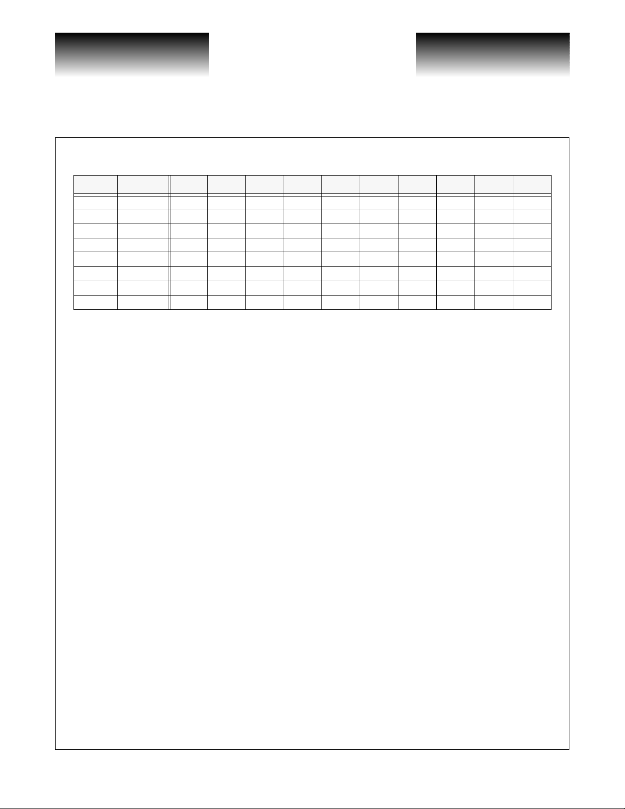
Table 3: DEMUX Mode DIN to SB Cross Reference
S<2:0> Modulus DIN9 DIN8 DIN7 DIN6 DIN5 DIN4 DIN3 DIN2 DIN1 DIN0
000 10 1:4 36-39 32-35 28-31 24-27 20-23 16-19 12-15 8-11 4-7 0-3
001 8 1:5 35-39 30-34 25-29 20-24 14-19 10-14 5-9 0-4
010 5 1:8 32-29 24-31 16-23 8-15 0-7
011 4 1:10 30-39 20-29 10-19 0-9
100 2 1:16 16-32 0-15
101 2 1:20 20-39 0-19
110 1 1:32 0-31
111 1 1:40 0-39
Preliminary Datash ee t
VSC6424
Initialization
The VSC6424 requires that the SYNC/SLDN input be low for at least one clock cycle after power on, then
be set high for at least on cloc k per i od to ini t ia li ze t he device. This is an edge sensitive function. In internal timing mode this serves to start the internal clock dividers and set the shift register and low speed output clocks in
motion. Additional edges while in internal timing mode serves to synchronize the output clocks as described
below. Once this has been done the device takes (2n) cycles to stabilize. During this time the slow bus (SB)
should be set to zero. The first data is then latched from the slow bus (SB) at the end of the (2n ) cycles. The
device is no w set to run and will lat ch data fro m the slo w b us (SB) every (n) cycl es. See Table 5 to determine (n)
for a selected modulus.
In MUX mode with internal timing the VSC6424 chip can also be initialized by providing a slow speed
clock to the SYNC input. This slow speed clock must be synchronized with high speed clock and based on the
modulus that the MUX is set to. For example if the VSC6424 is set to 4:1 mode and the high speed clock is set
to 500MHz then the SYNC input must be 125MHz. The initialization at power on will still take (2n) cycles of
the high speed clock. This allows the system to dictate when the slow speed data is latched and where the shifting begins.
In external timing mode the SLDN/SYNC signal serves to set the shift register in motion once the data has
been latched from the slow speed bus.
Page 4
741 Calle Plano, Camarillo, CA 93012 • 805/388-3700 • FAX: 805/987-5896 7/13/99
VITESSE
SEMICONDUCTOR CORPORATION G52236-0, Rev 3.0
VITESSE
SEMICONDUCTOR CORPORATION
Preliminary Datasheet
SC6424
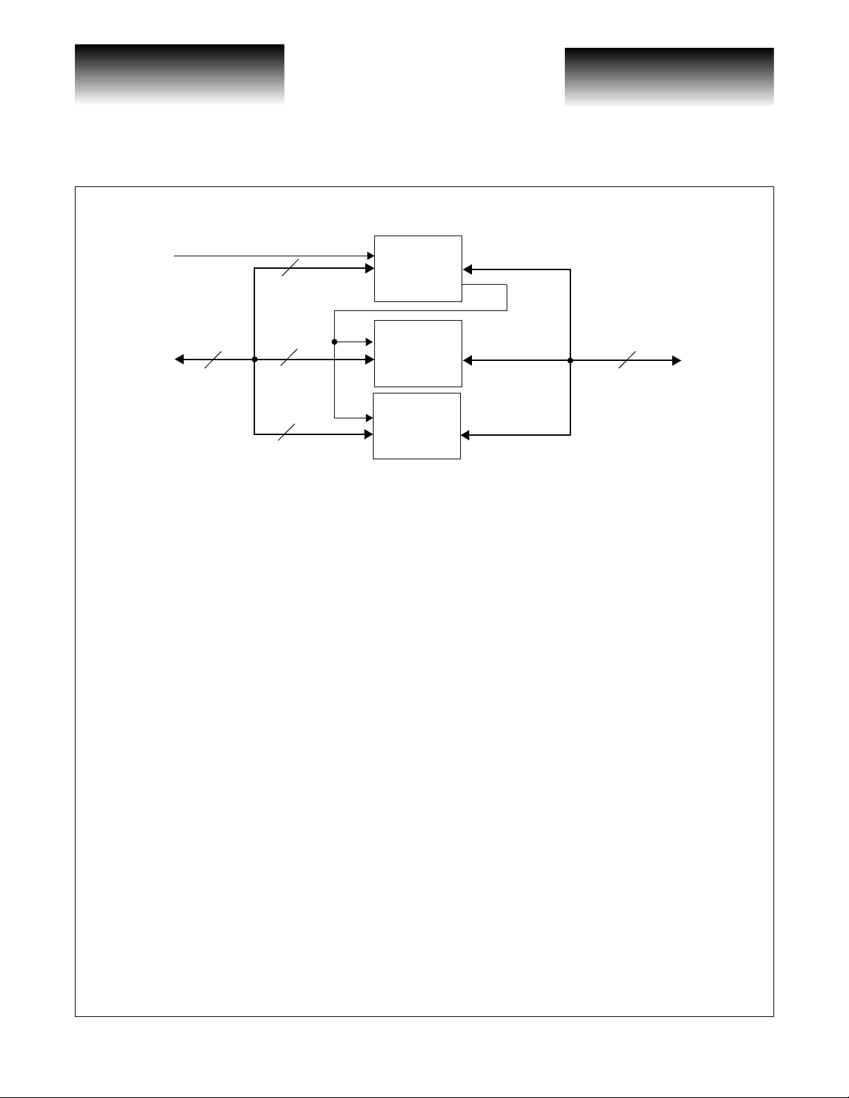
Figure 1: Synchronized VSC6424 Block Diagram
120
40
40
VSC6424
40
SLDN/SYNC
CLKT
VSC6424
SLDN/SYNC
3 - 30
VSC6424
SLDN/SYNC
500 Mb/s Video
Shift Register IC
Synchronization
Several VSC6424 chips can be synch roni zed t og eth er while in i nt er nal t iming mode by connecting the sl ow
speed TTL clock output (CLKT) of a master chip to the synchroni zation input (SYNC) of a slave chip. T he in ternal timing generator synchronize s to the rising edge of the SYNC input. Given that (n) is the number of high
speed clock cycles for a given modulus mode, synchronization takes two times (n) or (2n) clock cycles to lock
in. If it is necessary to synchroniz e more than two VSC64 24 devices use the TTL clock outpu t (CLKT) from
one chip to drive the SYNC inputs of each of the slave devices. See Figure 2 for a block diagram. See Figure 7
for a timing illustration of the synchronization timing of the slave chip. See Table 5 to determine (n) for a
selected modulus.
In MUX mode multiple VSC6424 chips can als o be sync hronized by pr oviding a slow speed clock to the
SYNC input on all of the devices. This slo w speed cl ock mu st be synchronized with high speed clock and b a sed
on the modulus that the MUX is set to. F or example if the VSC6424 is set to 8: 1 mod e and t he high speed clock
is set to 400MHz then the SYNC input must be 50MHz.
MPU Address Interface
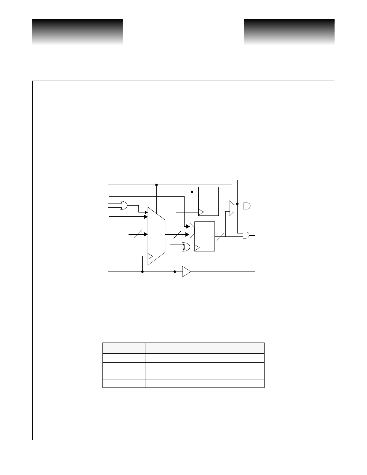
An Address Interface mode translates TTL compatible addresses to ECL compatible output levels. This is
provided for compatibility with the Bt424. When the Address Enable (AEN) signal is low, data from the
Address Line A<0:4> TTL input pins is transferred to the DOUT<0,2,4,6,7> ECL output pins with one clock
cycle delay. When AEN is high, the A<0:4> inputs are ignored. The DOUT<0:7> data is always synchronized
to CLK, regardless of the state of AEN. See Figure 9 for a timing illustration of this function.
Video Blanking
The VSC6424 also has a blanking functi on for video appli cations. I n multip le xe r mode, thi s functi on all o ws
zeroing of the high speed outputs (DOUT<0:7>). Setting HBLANK or VBLANK low drives all DOUT<0:7>
outputs low synchro nously wit h th e clock (CLK). The outputs will be driven low on the modulus boundary. The
outputs are driven low for (n) clock cycles given that (n) is the modulus mode that the chip is set to. See table 4
to determine the value of (n) for a given modulus.
G52236-0, Rev 3.0
7/13/99 741 Calle Plano, Camarillo, CA 93012 • 805/388-3700 • FAX: 805/987-5896
VITESSE
SEMICONDUCTOR CORPORATION Page 5
VITESSE
SEMICONDUCTOR CORPORATION
00 Mb/s Video
hift Register IC
Preliminary Datash ee t
VSC6424
HBLANK or VBLANK must be driven low for at least one clock cycle two clock cycles before the desired
point of blanking. See Figure 6 for a timing illustration of this function.
Retimer
The chip also contains a retime r function. This fun ction works in DEMUX mode. The RETIME signal is
routed to DOUT<7> through a flip-flop. The flip-flop is internally clocked by the low speed ECL output clock
(CLKE). This function is depicted in the detailed block diagram (Figure 3) below. See Figure 5 for a timing
illustration.
Figure 2: Multiplexer Detailed Block Diagram
OEN
MODE
AEN/RETIME
A<0:4>
HBLANK
VBLANK
S<0:2>
OPS
CLK
40
MUX
CLKE
8
Retimer
Output
Latch
DOUT<7>
7
8
DOUT<0:6>
High
Speed
Interface
(ECL)
CLKOUT
Termination
It is recommended to leave all unused ECL outputs floating. It is recommended that unused ECL inputs be
terminated low (-2V supply). Refer t o th e following table recommended input termination for all levels.
Table 4: Input Termination Recommendations
Type State Input
ECL High ground via a diode
ECL Low -2V supply
TTL High +3.3V supply
TTL Low Ground
Page 6
741 Calle Plano, Camarillo, CA 93012 • 805/388-3700 • FAX: 805/987-5896 7/13/99
VITESSE
SEMICONDUCTOR CORPORATION G52236-0, Rev 3.0
 Loading...