


VITESSE
SEMICONDUCTOR CORPORATION
Data Sheet
VSC6250
Features
• High-Speed Operation:
1 Gb/s Data Rate
500ps min Output Pulse Width
750ps min Input Pulse Width
• Excellent Overall Timing Accuracy:
Ultra-Stable Timing Delays
Minimum Pattern Dependence
Very Fine Timing Resolution (1 LSB = 8ps)
• High Level of Integration Reduces Board Area:
16 Independently Adjustable Delay Lines in a
Single Package
• Configurable as 2 1:8 or 1:16
1Gb/s 16-Channel
Drive-Side Deskew IC
• Wide Span: > 4ns Usable Range
• Pulse Width Adjustment to Compensate for
Dispersion in Pin Electronics:
± 2ns Independent Adjustment of Rising and
Falling Edges
• Fully Digital Single-Chip Solution:
No Off-Chip DACs Required
No DAC-Induced Timing Errors from Analog
Crosstalk, Reference Noise, Temperature, or
Voltage Drift
• Single Power Supply: -2V @ 5W
• 128-Pin PQFP, 14x20mm ThermallyEnhanced Package
Applications
• Drive-Side Deskew in High-Speed Memory
Testers
• Direct RAMBUS DRAM, SLDRAM, DDR
SDRAM, Fast SSRAM
• High-Speed Instrumentation: Pulse Generators,
Timing Margin Testers for Datalink, Interface,
and Disk Drive Applications
• Telecom, Datacom, and Computer Deskew
General Description
The VSC6250 is intended for use in the next generation o f high-speed, high-accurac y memory testers for
devices such as Direct RAMBUS DRAM, SLDRAM, DDR SDRAM, and fast SSRAM.
The VSC6250 provides ultra-precise timing to allow next genera tion memory tes ters to achieve excellent
overall timing accuracy. Timing delays of the VSC6250 are extremely stable with r espect to temperatu re and
voltage. Proprietar y circuit desi gn and process te chnology red uce pattern, data, frequency, and duty-cycle
dependencies to an absolute minimum. The VSC6250 requires no external DACs, which eliminates errors due
to DAC reference noise and analog crosstalk, and DAC temperature and voltage drift. The VSC6250 is available in a 128-pin PQFP, 14x20mm thermally-enhanced package.
G52197-0, Rev. 4.0
8/19/00 741 Calle Plano, Camarillo, CA 93012 • 805/388-3700 • FAX: 805/987-5896
VITESSE SEMICONDUCTOR CORPORATION
Page 1

VITESSE
SEMICONDUCTOR CORPORATION
1Gb/s 16-Channel
Drive-Side Deskew IC
VSC6250 Block Diagram
DINA
DIN
DINB
Data Sheet
VSC6250
S
R
S
R
S
R
Output 0
Output 7
Output 8
Reference
Clock
(250MHz)
Stability
Control
Parallel Data Interface
S
R
Output 15
Page 2
741 Calle Plano, Camarillo, CA 93012 • 805/388-3700 • FAX: 805/987-5896 8/19/00
VITESSE SEMICONDUCTOR CORPORATION
G52197-0, Rev. 4.0
VITESSE
SEMICONDUCTOR CORPORATION
Data Sheet
VSC6250
1Gb/s 16-Channel
Drive-Side Deskew IC
Functional Description
The VSC6250 is a 1Gb/s 16- channel drive-path deskew IC desi gned for deske wing differences in path
delay between multiple DUTs in a high-speed memory test system. The VSC6250 can be used as two independent 1:8 fanout and deskew sections or as a single 1:16 fanout and deskew. When used as two 1:8 deskews,
input signals are applied to inputs DINA and DINB. When used as a single 1:16 deskew, the input is applied to
input DIN.
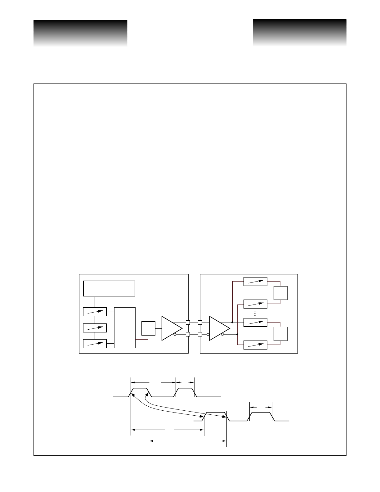
The VSC6250 is designed to operate with a conventional 500MHz timing generator which outputs formatted pulses to the VSC6250 deskew IC. See Figure 1. The waveform at the input of the VSC6250 is the same as
that presented to the DUT pin. In a memory tester, such a 500MHz timing generator IC may be designed:
• Using one edge to output a single 500Mb/s data stream
• Using two edges to output a single 500Mb/s data stream preceded its complement
• Using three edges to output a single data stream at 500Mb/s surrounded by its complement
• Using two edges to output two interleaved 500Mb/s data streams for an aggregate bandwidth of 1Gb/s.
Formatting is performed inside the timing generator IC. An example interface between the timing generator
IC and the deskew is shown in Figure 1. This configuration is capable of supporting the four different data output choices, with appropriate design of the formatting logic.
The VSC6250 can handle pulses with a data rate up to 1Gb/s or a pulse repetition rate up to 2ns. A timing
diagram for the VSC6250 is shown in Figure 2.
Figure 1: VSC6250 Interface to Timing Generator IC
Timing Generator VSC6250
Timeset/Dataset
RAM
Format
Logic
DINx
DOUTx
S
R
Figure 2: VSC6250 AC Timing Diagram
t
REFIRE
t
PDR
t
PWI
t
PDF
t
S
R
S
R
PWO
G52197-0, Rev. 4.0
8/19/00 741 Calle Plano, Camarillo, CA 93012 • 805/388-3700 • FAX: 805/987-5896
VITESSE SEMICONDUCTOR CORPORATION
Page 3
VITESSE
SEMICONDUCTOR CORPORATION
1Gb/s 16-Channel
Drive-Side Deskew IC
The delay of each of the deskewed outputs can be adjusted separately to compensate for differences in path
length between DUTs on a single test head. The maximum delay is 7ns. Delay span is 5ns. Usable range is a
minimum of 4ns
and falling edges can be adjusted independently.
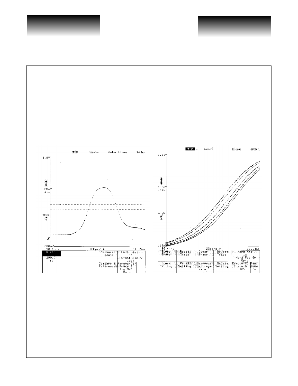
To ensure timing performance, delay of the VSC6250 is measured in product ion at every time ste p of every
vernier. Figure 3 shows measured output waveforms of the VSC6250. Figure 3 (a) shows a measured minimum
output pulse width. The specified mimi mum outpu t pulse wi dth is 500ps, but this measu rement shows operat ion
down to 300ps. Figure 3 (b) shows typical timing resolution of 8ps.
(1).
Resolution is 8ps. To compensate for pulse dispersion in pin electronics, delay of the rising
Figure 3: VSC6250 Measured Output Waveforms
Data Sheet
VSC6250
a) Mininum output pulse width of 300ps (b) Typical timing resolution of 8ps
With next generation testers required to test more DUTs per testhead in the same footprint, board area is a
critical design parameter. Providing 16 deskew channels in a 14mmx20mm thermally-enhanced 128-pin PQFP
package, the VSC6250 consumes less than 1/2 the total board area of the bipolar alternative.
Page 4
741 Calle Plano, Camarillo, CA 93012 • 805/388-3700 • FAX: 805/987-5896 8/19/00
VITESSE SEMICONDUCTOR CORPORATION
G52197-0, Rev. 4.0

VITESSE
SEMICONDUCTOR CORPORATION
Data Sheet
VSC6250
1Gb/s 16-Channel
Drive-Side Deskew IC
The 32 delays (rising and falling edges for 16 channels) in the VSC6250 are programmed using a parallel
interface. Verniers are selected by a 5-bit address word and controlled by two function enable bits. Each vernier
requires 11 bits to set the delay value.
Power dissipation of the VSC6250 is less than 5W from a single -2V supply.
Table 1: Operational Mode Truth Table
Mode # Mode Name CALENN Mode Description
1Cal Mode 0
2 User Mode 1 Generates timing delays as set by data in Cal Mode.
Figure 4: CAL Mode Timing Diagram
ADR[4:0]
CALENN
Sets timing delays with each vernier selected with ADR [3:0] Serial Data
Input.
D[10:0]
MSB LSB
Load Calibration Register
Data Latch Transparent
1 CAL Cycle
Don’t Care
Latch Data into Data Latch
Measure Delay
10 9
G52197-0, Rev. 4.0
8/19/00 741 Calle Plano, Camarillo, CA 93012 • 805/388-3700 • FAX: 805/987-5896
VITESSE SEMICONDUCTOR CORPORATION
Page 5
VITESSE
SEMICONDUCTOR CORPORATION
1Gb/s 16-Channel
Drive-Side Deskew IC
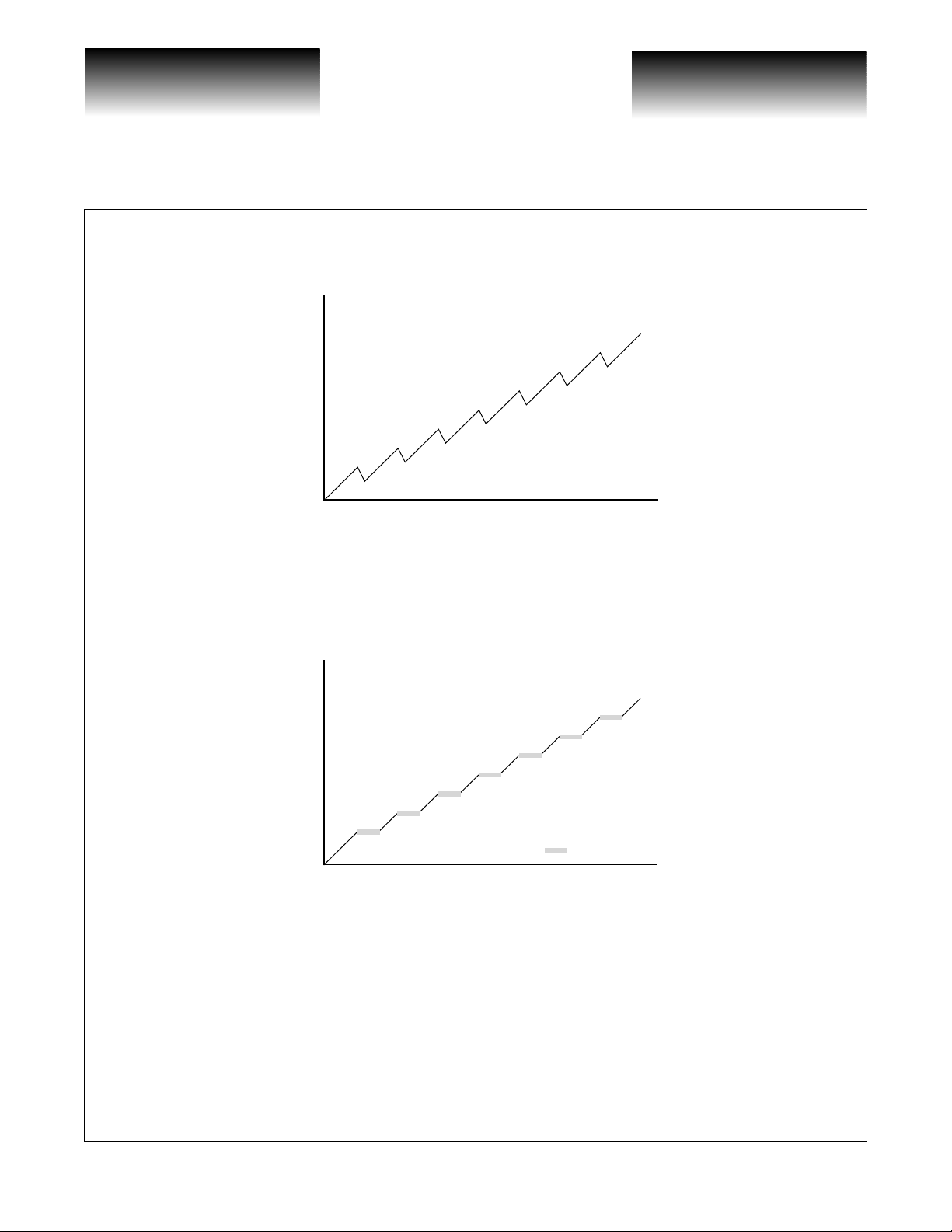
Figure 5: CAL Mode: Pre-Calibration Delay Range
32 Coarse Vernier Steps +
64 Fine Vernier Steps
Delay
000 Delay[0:10]
Figure 6: CAL Mode: Post-Calibration Delay Range
(1)
~275ps Fine Vernier Range
Data Sheet
VSC6250
32 Coarse Vernier Steps +
64 Fine Vernier Steps
Delay
000 Delay[0:10]
NOTE: (1) There are 32 coarse vernier codes and 64 fine vernier codes. Not all of the codes are used to reach
maximum delay. The current design utilizes 22 coarse cod es and 47 fine vern ie r code s. Fu tu re de sign s will utilize 22
course designs and 59 fine vernier codes. These numbers must be used whe n calculating INL and DNL. S yst em calibration should be performed with the maximum usable codes. When a code is programmed beyond the maximum
utilized code, the delay will toggle between maximum delay and maximum delay minus 1LSB. Please contact your
local Vitesse sales representative to determine when the future design will be available.
(1)
= Unused Codes
Page 6
741 Calle Plano, Camarillo, CA 93012 • 805/388-3700 • FAX: 805/987-5896 8/19/00
VITESSE SEMICONDUCTOR CORPORATION
G52197-0, Rev. 4.0

VITESSE
SEMICONDUCTOR CORPORATION
Data Sheet
VSC6250
1Gb/s 16-Channel
Drive-Side Deskew IC
AC Timing Characteristics
Table 2: AC Timing Characteristics
Parameter Description Min Typ Max Units
t
PDR(MIN), tPDF(MIN)
t
PDR(MAX), tPDF(MAX)
t
PD(SPAN)
t
RES
DNL Delay Differential Nonlinearity -2 — +2 LSB
t
PWI
t
PWO
FRCK Reference Clock Frequency 250 — MHz
DTDD Variation in Delay vs. Duty Cycle -50 — +5 0 ps
DTDT Variation in Delay vs Temperature — 2 — ps/C°
PSRR Power Supply Rejection Ratio
t
R/tF
t
REFIRE
J
O
Propagation Delay, Minimum Delay 4.1 5 6.5 ns
Propagation Delay, Maximum Delay 9.9 11.6 13.5 ns
Propagation Delay, Span 5.8 —7 ns
Delay Element Resolution — 8 20 ps
Input Pulse Width 0.75 — — ns
Output Pulse Width 0.5 — — ns
(1)
Output Rise Fall Times (20% to 80%) — 300 — ps
Adjacent Edge Spacing 2 — — ns
Output Jitter — 3 — p s rms
— — 230 ps/100mV
NOTE: (1) Change in range of maximum delay.
.
DINx
DOUTx
Figure 7: AC Timing Diagram
t
PDF(MAX)
t
PDF(MIN)
t
PDR(MAX)
t
PDR(MIN)
t
PDR(SPAN)
t
PWO
t
PDF(SPAN)
G52197-0, Rev. 4.0
8/19/00 741 Calle Plano, Camarillo, CA 93012 • 805/388-3700 • FAX: 805/987-5896
VITESSE SEMICONDUCTOR CORPORATION
Page 7

VITESSE
SEMICONDUCTOR CORPORATION
1Gb/s 16-Channel
Drive-Side Deskew IC
DC Characteristics
Table 3: Single Ended ECL Inputs and Outputs
Parameter Description Min Typ Max Units Conditions
V
OH
VOLOutput LOW Voltage -2000 — -1620 mV
V
IH
V
IL
I
IH
I
IL
NOTE: VTT = -2.0V ± 5%, VCC = V
Table 4: Differential ECL Inputs and Outputs
Parameter Description Min Typ Max Units Conditions
V
INDIFF
V
INCM
V
OUTDIFF
V
OUTCM
Output HIGH Voltage -1020 —-700mV
Input HIGH Voltage -1165 — -700 mV
Input LOW Voltage -2000 — -1475 mV
Input HIGH Current - — 200 µ A V
Input LOW Current -50 — — µA V
= GND, R
CCA
Input Voltage Differential 200 — — mV
Input Common-Mode Voltage -1.5 — -0.5 V
Output Voltage Differential 400 — — mV Output voltage swing
Output Common-Mode Voltage -1.5 — -0.7 V
= 50Ω to -2.0V, external reference (V
LOAD
IN
IN
) = -1.32V ± 25mV.
REF
Required for full
output swing
Common-mode range
required for full output
swing with V
applied
Common-mode output
voltage
Data Sheet
VSC6250
= VIH (max)
= VIL (min)
DIFF
Table 5: VSC6250 Power Dissipation
Parameter Description Min Typ Max Units Conditions
I
TT
P
D
NOTE: (1) Output power dissipation does not include load power.
Page 8
VTT Supply Current — 2000 2870 mA
Power Dissipation
741 Calle Plano, Camarillo, CA 93012 • 805/388-3700 • FAX: 805/987-5896 8/19/00
(1)
VITESSE SEMICONDUCTOR CORPORATION
—4 6 W
G52197-0, Rev. 4.0

VITESSE
SEMICONDUCTOR CORPORATION
Data Sheet
VSC6250
Absolute Maximum Ratings
Power Supply Voltage (VTT) ...........................................................................................................-2.5V to +0.5V
ECL Input Voltage Applied, (V
Output Current (I
Case Temperature Under Bias (T
Storage Temperature (T
) ....................................................................................................................................50mA
OUT
STG
IN ECL
).............................................................................................-55oC to + 125oC
C
).........................................................................................................-65oC to + 150oC
(1)
)................................................................................. +0.5V to VTT + -0.5V
1Gb/s 16-Channel
Drive-Side Deskew IC
Recommended Operating Conditions
Power Supply Voltage (VTT).................................................................................................................-2.0V ± 5%
Commercial Operating Temperature Range
NOTES: (1) CAUTION: Stresses listed un de r “Ab solute Maximum Ratin gs” m a y be ap plied to devices one at a t im e without caus-
ing permanent damage. Functionality at or above the values listed is not implied. Exposure to these values for extended
periods may affect device reliability.
(2) Lower limit of specification is ambient temperature and upper limit is case temperature.
(2)
(T) ............................................................................ 30oC to 70oC
ESD Ratings
Proper ESD procedures should be used when handling this product. The VSC6250 is rated to the following
ESD voltages based on the human body model:
1. All pins are rated at or above 1500V.
G52197-0, Rev. 4.0
8/19/00 741 Calle Plano, Camarillo, CA 93012 • 805/388-3700 • FAX: 805/987-5896
VITESSE SEMICONDUCTOR CORPORATION
Page 9

VITESSE
SEMICONDUCTOR CORPORATION
1Gb/s 16-Channel
Drive-Side Deskew IC
Package Information
VTT
VDD
DOUT7
DOUT7N
VDD
DOUT6
DOUT6N
VTT
DOUT5
DOUT5N
VDD
DOUT4
DOUT4N
VDD
RCK
RCKN
VDD
VTT
VTT
VTT
DOUT3
DOUT3N
VDD
DOUT2
DOUT2N
VDD
DOUT1
DOUT1N
VDD
DOUT0
DOUT0N
VTT
VTT
VTT
VDD
ADR4
ADR3
VDD
1
2
3
4
5
6
7
8
9
10
11
12
13
14
15
16
17
18
19
20
21
22
23
24
25
26
27
28
29
30
31
32
33
34
35
36
37
38
VDD
128
VTT
CHPRST
127
126
VDD
125
ASYNCRST
VTT
VTT
DATA10
124
123
122
Figure 8: Pin Diagram
DATA9
VDD
DATA8
DATA7
DATA6
DATA5
VTT
VTT
VDD
121
120
119
118
117
116
115
114
113
112
VDD
111
VDD
DATA4
DATA3
DATA2
110
109
108
VSC6250
VTT
DATA1
DATA0
VDD
107
106
105
104
103
VITESSE
102
101
100
99
98
97
96
95
94
93
92
91
90
89
88
87
86
85
84
83
82
81
80
79
78
77
76
75
74
73
72
71
70
69
68
67
66
65
Data Sheet
VSC6250
CALENN
VREF
VTT
NC
NC
VDD
VTT
VDD
VTT
VDD
DOUT8N
DOUT8
VTT
DOUT9N
DOUT9
VDD
DOUT10N
DOUT10
VTT
DOUT11N
DOUT11
VDD
DOUT12N
DOUT12
VTT
DOUT13N
DOUT13
VDD
DOUT14N
DOUT14
VTT
DOUT15N
DOUT15
VDD
NC
VDD
VTT
VTT
39404142434445464748495051525354555657585960616263
ADR2
ADR1
Page 10
741 Calle Plano, Camarillo, CA 93012 • 805/388-3700 • FAX: 805/987-5896 8/19/00
VTT
VTT
ADR0
VTT
DINA
DINAN
DINN
DIN
VDD
DINB
DINBN
VDD
VDD
NC
ECLHI
VTT
VTT
VTT
VDD
VITESSE SEMICONDUCTOR CORPORATION
VTT
VTT
VTT
NC
64
NC
G52197-0, Rev. 4.0

VITESSE
SEMICONDUCTOR CORPORATION
Data Sheet
VSC6250
Table 6: Pin Identifications
Pin # Signal Name Signal Type Levels Description
1VTT — -2.0V Power Supply
2 VDD — 0V Ground
3 DOUT7 O ECL Output Channel 7, True
4 DOUT7N O ECL Output Channel 7, Complementary
5 VDD — 0V Ground
6 DOUT6 O ECL Output Channel 6, True
7 DOUT6N O ECL Output Channel 6, Complementary
8 VTT — -2.0V Power Supply
9 DOUT5 O ECL Output Channel 5, True
10 DOUT5N O ECL Output Channel 5, Complementary
11 VDD — 0V Power Supply
12 DOUT4 O ECL Output Channel 4, True
13 DOUT4N O ECL Output Channel 4, Complementary
14 VDD — 0V Ground
15 RCK I ECL 250 MHz Reference Clock, True
16 RCKN I ECL 250 MHz Reference Clock, Complementary
17 VDD — 0V Ground
18 VTT — -2.0V Power Supply
19 VTT — -2.0V Power Supply
20 VTT — -2.0V Power Supply
21 DOUT3 O ECL Output Channel 3, True
22 DOUT3N O ECL Output Channel 3, Complementary
23 VDD — 0V Ground
24 DOUT2 O ECL Output Channel 2, True
25 DOUT2N O ECL Output Channel 2, Complementary
26 VDD — 0V Ground
27 DOUT1 O ECL Output Channel 1, True
28 DOUT1N O ECL Output Channel 1, Complementary
29 VDD — 0V Ground
30 DOUT0 O ECL Output Channel 0, True
31 DOUT0N O ECL Output Channel 0, Complementary
32 VTT — -2.0V Power Supply
33 VTT — -2.0V Power Supply
34 VTT — -2.0V Power Supply
35 VDD — 0V Ground
36 ADR4 I ECL Address Bit 4 for Vernier Selection
37 ADR3 I ECL Address Bit 3 for Vernier Selection
1Gb/s 16-Channel
Drive-Side Deskew IC
G52197-0, Rev. 4.0
8/19/00 741 Calle Plano, Camarillo, CA 93012 • 805/388-3700 • FAX: 805/987-5896
VITESSE SEMICONDUCTOR CORPORATION
Page 11

VITESSE
SEMICONDUCTOR CORPORATION
1Gb/s 16-Channel
Drive-Side Deskew IC
Pin # Signal Name Signal Type Levels Description
38 VDD — 0V Ground
39 ADR2 I ECL Address Bit 2 for Vernier Selection
40 ADR1 I ECL Address Bit 1 for Vernier Selection
41 VTT — -2.0V Power Supply
42 ADR0 I ECL Address Bit 3 for Vernier Selection
43 VTT — -2.0V Power Supply
44 VTT — -2.0V Power Supply
45 DINAN I ECL Input A, Complementary
46 DINA I ECL Input A, True
47 DINN I ECL Common Input, Complementary
48 DIN I ECL Common Input, True
49 VDD — 0V Ground
50 DINBN I ECL Input B, Complementary
51 DINB I ECL Input B, True
52 VDD — 0V Ground
53 VDD — 0V Ground
54 ECLHI O ECL ECL High V olt age
55 NC — — Not Connected
56 VTT — -2.0V Power Supply
57 VTT — -2.0V Power Supply
58 VTT — -2.0V Power Supply
59 VDD — 0V Ground
60 VTT — -2.0V Power Supply
61 VTT — -2.0V Power Supply
62 VTT — -2.0V Power Supply
63 NC — 0V Not Connected
64 NC — 0V Not Connected
65 VTT — -2.0V Power Supply
66 VTT — -2.0V Power Supply
67 VDD — 0V Ground
68 NC — 0V Not Connected
69 VDD — 0V Ground
70 DOUT15 O ECL Output Channel 15, True
71 DOUT15N O ECL Output Channel 15, Complementary
72 VTT — -2.0V Power Supply
73 DOUT14 O ECL Output Channel 14, True
74 DOUT14N O ECL Output Channel 14, Complementary
75 VDD — 0V Ground
Data Sheet
VSC6250
Page 12
741 Calle Plano, Camarillo, CA 93012 • 805/388-3700 • FAX: 805/987-5896 8/19/00
VITESSE SEMICONDUCTOR CORPORATION
G52197-0, Rev. 4.0

VITESSE
SEMICONDUCTOR CORPORATION
Data Sheet
VSC6250
Pin # Signal Name Signal Type Levels Description
76 DOUT13 O ECL Output Channel 13, True
77 DOUT13N O ECL Output Channel 13, Complementary
78 VTT — -2.0V Power Supply
79 DOUT12 O ECL Output Channel 12, True
80 DOUT12N O ECL Output Channel 12, Complementary
81 VDD — 0V Ground
82 DOUT11 O ECL Output Channel 11, True
83 DOUT11N O ECL Output Channel 11, Complementary
84 VTT — -2.0V Power Supply
85 DOUT10 O ECL Output Channel 10, True
86 DOUT10N O ECL Output Channel 10, Complementary
87 VDD — 0V Ground
88 DOUT9 O ECL Output Channel 9, True
89 DOUT9N O ECL Output Channel 9, Complementary
90 VTT — -2.0V Power Supply
91 DOUT8 O ECL Output Channel 8, True
92 DOUT8N O ECL Output Channel 8, Complementary
93 VDD — 0V Ground
94 VTT — -2.0V Power Supply
95 VDD — 0V Ground
96 VTT — -2.0V Power Supply
97 VDD — 0V Ground
98 NC — — Not Connected
99 NC — — Not Connected
100 VTT — -2.0V Power Supply
101 VREF DC -1.32V ECL Reference Voltage
102 CALENN I ECL Write Delay Register
103 VDD — 0V Ground
104 DATA0 I ECL Delay Bit 0
105 DATA1 I ECL Delay Bit 1
106 VTT — 0V Power Supply
107 DATA2 I ECL Delay Bit 2
108 DATA3 I ECL Delay Bit 3
109 DATA4 I ECL Delay Bit 4
110 VDD — 0V Ground
111 VDD — 0V Ground
112 VDD — 0V Ground
113 VTT — -2.0V Power Supply
114 VTT — -2.0V Power Supply
1Gb/s 16-Channel
Drive-Side Deskew IC
G52197-0, Rev. 4.0
8/19/00 741 Calle Plano, Camarillo, CA 93012 • 805/388-3700 • FAX: 805/987-5896
VITESSE SEMICONDUCTOR CORPORATION
Page 13

VITESSE
SEMICONDUCTOR CORPORATION
1Gb/s 16-Channel
Drive-Side Deskew IC
Pin # Signal Name Signal Type Levels Description
115 DATA5 I ECL Delay Bit 5
116 DATA6 I ECL Delay Bit 6
117 DATA7 I ECL Delay Bit 7
118 DATA8 I ECL Delay Bit 8
119 VDD — 0V Ground
120 DATA9 I ECL Delay Bit 9
121 DATA10 I ECL Delay Bit 10
122 VTT — -2.0V Power Supply
123 VTT — -2.0V Power Supply
124 ASYNCRST I ECL
125 VDD — 0V Ground
126 CHPRST I ECL
127 VTT — -2.0V Power Supply
128 VDD — 0V Ground
Data Sheet
VSC6250
Asynchronously reset s all vernier outputs to l ogic
LOW.
Chip Reset. Resets all vernier outputs to LOW a nd
initializes all delay registers to zero.
Page 14
741 Calle Plano, Camarillo, CA 93012 • 805/388-3700 • FAX: 805/987-5896 8/19/00
VITESSE SEMICONDUCTOR CORPORATION
G52197-0, Rev. 4.0

VITESSE
SEMICONDUCTOR CORPORATION
Data Sheet
VSC6250
Package Information
1Gb/s 16-Channel
Drive-Side Deskew IC
128-Pin Thermally-Enhanced PQFP
Body + 3.2mm Footprint, 2.70mm Thick
DIMENSIONS LEADS TOLERANCES
A
A
A
D
D1
E
E
L
e
b
θ
θ
ddd
ccc
3.40
0.25 / 0.50
2.70
17.20
14.00
23.20
20.00
0.88
0.50
0.22
0˚ - 7˚
6˚
0.8 MAX.
0.08
1
2
1
1
MAX.
MIN./MAX.
±0.10
±0.20
±0.10
±0.20
±0.10
+0.15 / –0.10
BASIC
±0.05
±4˚
MAX.
G52197-0, Rev. 4.0
NOTES:
1) All dimensions in mm.
2) Dimensions shown are
nominal with tolerances as indicated.
3) Foot length "L" is measure at gage
plane, 0.25 above the seating plane.
VITESSE SEMICONDUCTOR CORPORATION
8/19/00 741 Calle Plano, Camarillo, CA 93012 • 805/388-3700 • FAX: 805/987-5896
Page 15

VITESSE
SEMICONDUCTOR CORPORATION
1Gb/s 16-Channel
Drive-Side Deskew IC
Data Sheet
VSC6250
Package Thermal Characteristics
The VSC6250 is packaged in an 128-pin, 14x20mm thermally-enhanced PQFP with an internal heat
spreader. These packages use industry-standard EIAJ footprints, which have been enhanced to improve thermal
dissipation. The construction of the packages are as shown in Figure 9. The VSC6250 is designed to operate
with a case temperature up to 90
Exposed Heat Slug
Insulator
Wire Bond
o
C. The user must guarantee that the temperature specification is not violated.
Figure 9: Package Cross Section
Plastic Molding Compound
Lead
Thermal Epoxy
Die
Table 7: Thermal Resistance
Symbol Description Value Units
θ
θ
CA-0
θ
CA-100
θ
CA-200
θ
CA-400
θ
CA-600
θ
CA-800
JC
Thermal resistance from junction-to-case 6.6
Thermal resistance from case-to-ambient, st ill air 23
Thermal resistance from case-to-ambient, 100 LFPM air 21
Thermal resistance from case-to-ambient, 200 LFPM air 19.9
Thermal resistance from case-to-ambient, 400 LFPM air 18
Thermal resistance from case-to-ambient, 600 LFPM air 17.3
Thermal resistance from case-to-ambient, 800 LFPM air 16.6
o
C/W
o
C/W
o
C/W
o
C/W
o
C/W
o
C/W
o
C/W
Page 16
741 Calle Plano, Camarillo, CA 93012 • 805/388-3700 • FAX: 805/987-5896 8/19/00
VITESSE SEMICONDUCTOR CORPORATION
G52197-0, Rev. 4.0

VITESSE
SEMICONDUCTOR CORPORATION
Data Sheet
VSC6250
Ordering Information
The part number for this product is formed by a combination of the device type and the package style:
Device Type
1Gb/s 16-Channel Drive-Side Deskew IC
VSC6250
1Gb/s 16-Channel
Drive-Side Deskew IC
xx
Package
QW: 128-Pin, 14x20mm Body
Notice
Vitesse Semiconductor Corporation reserves the right to make changes in its products, specifications, or
other information at any time without prior notice. Therefore the reader is cautioned to confirm that this data
sheet is current prior to placing any orders. The Company assumes no responsibility for any circuitry described
other than circuitry entirely embodied in a Vitesse product.
Warning
Vitesse Semiconductor Corporation’s products are not intended for use in life support appliances, devices
or systems. Use of a Vitesse product in such applications without written consent is prohibited.
G52197-0, Rev. 4.0
8/19/00 741 Calle Plano, Camarillo, CA 93012 • 805/388-3700 • FAX: 805/987-5896
VITESSE SEMICONDUCTOR CORPORATION
Page 17

VITESSE
SEMICONDUCTOR CORPORATION
1Gb/s 16-Channel
Drive-Side Deskew IC
Data Sheet
VSC6250
This page left intentionally blank.
Page 18
741 Calle Plano, Camarillo, CA 93012 • 805/388-3700 • FAX: 805/987-5896 8/19/00
VITESSE SEMICONDUCTOR CORPORATION
G52197-0, Rev. 4.0
 Loading...