

VITESSE VSC6112, VSC6108, VSC6110 Datasheet
VITESSE
SEMICONDUCTOR CORPORATION
Advance Product Information
VSC6108/10/12
Low Jitte
r
Clock Multiplier and Distributo
r
G52224-0, Rev 2.1
VITESSE SEMICONDUCTOR CORPORATION
Page 1
2/15/99
741 Calle Plano, Camarillo, CA 93012 • 805/388-3700 • FAX: 805/987-5896
Features
General Description
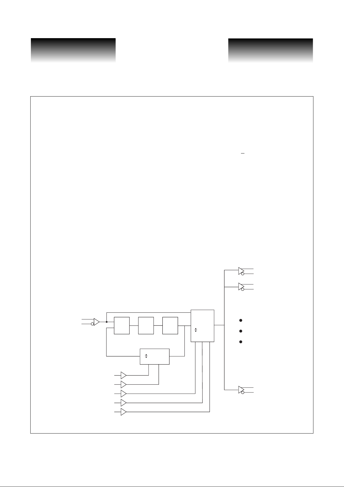
The VSC6108/10/12 are a family of low-jitter clock multiplication and distribution ICs. Each IC uses a
phase locked-loop to lock an on-chip low-noise VCO to an off-chip reference frequency. The VCO output can
be divided down and is output to 18 differential ECL outputs. The VSC6108/10/12 are packaged in a 10 mm x
10 mm 64-pin plastic quad flat pack and consume less than 2 Watts from a single 3.3V power supply.
The VSC6108/10/12 provide high-precision clocks for ATE, instrumentation, telecommunications, datacommunications, and computer system applications where jitter and skew are critical timing parameters. Skew
between outputs is less than 50 ps. Jitter is less than 4 ps rms or 25 ps peak-to-peak. Lock time is 10 µs.
VSC6108/10/12 Functional Block Diagram
• Recommended Companion for VSC6250 500MHz
Deskew IC and Vitesse Timing Generator ICs
• Input Clock Frequency: 50MHz to 622MHz
• Output Clock Frequency: 100MHz to 1.25GHz
• 1 Differential ECL or PECL Clock Input
• 18 Differential ECL or PECL Clock Outputs
• Very Low Jitter: 4ps rms, 25ps Peak-to-Peak
• 10µs Lock Time
• < 50ps Skew Between Outputs
• Single Supply: 3.3V +
5% @ 2 Wa tt s
• Commercial (0
o
to +70oC) Temperature Range
• Package: 10mm x 10mm 64 PQFP
IN
INN
OUT0
OUT0N
OUT1
OUT1N
OUT17
OUT17N
VCO
Loop
Filter
Phase
Detector
Bypass
2,4,8,16
4,8,16,32
FISEL1
FISEL0
FOSEL2
FOSEL1
FOSEL0
VITESSE
SEMICONDUCTOR CORPORATION
Advance Product Information
VSC6108/10/12
Low Jitter
C
lock Multiplier and Distributor
Page 2
VITESSE SEMICONDUCTOR CORPORATION
G52224-0, Rev 2.1
741 Calle Plano, Camarillo, CA 93012 • 805/388-3700 • FAX: 805/987-5896
2/15/99
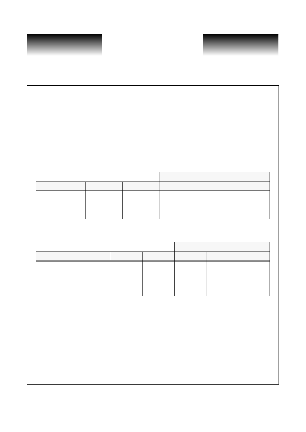
Three versions of the clock multiplier and distributor IC are available.
1. The VSC6108 has a VCO frequency of 1.6 GHz and can output clocks at 800 MHz, 400 MHz, 200 MHz,
and 100 MHz.
2. The VSC6110 has a VCO frequency of 2.0 GHz and can output clocks at 1 GHz, 500 MHz, 250 MHz, and
125 MHz.
3. The VSC6112 h as a VCO frequency of 2. 488 GHz and can o utput clocks at 1.244GHz, 622 MHz, 311MHz,
and 155MHz.
VCO multiplication and ou t put di vi sion ratios a re use r-selectable . Each of the ICs can be co nfig u red for an
input frequency of 1/ 4, 1/8, 1/16, or 1/32 of the VCO fr equency as shown in Table 1 below. The output frequencies are selected as shown in Table 2 below.
Table 1: Input Frequency vs. Mode
Table 2: Output Frequency vs. Mode
f
IN
Mode Name FISEL1 FISEL0 VSC6108 VSC6110 VSC6112
f
VCO
= fIN * 4 0 0 400 MHz 500 MHz 6 22 MHz
f
VCO
= fIN * 8 0 1 200 MHz 250 MHz 311 MHz
f
VCO
= fIN * 16 1 0 100 MHz 125 MHz 155 MHz
f
VCO
= fIN * 32 1 1 50 MHz 62.5 MHz 77.5 MHz
f
OUT
Mode Name FOSEL2 FOSEL1 FOSEL0 VSC6108 VSC6110 VSC6112
f
OUT
= f
IN
000 fIN f
IN
f
IN
f
OUT
= f
VCO
/ 2 0 0 1 800 MHz 1 GHz 1.244GHz
f
OUT
= f
VCO
/ 4 0 1 0 400 MHz 500 MHz 622 MHz
f
OUT
= f
VCO
/ 8 0 1 1 200 MHz 250 MHz 311 MHz
f
OUT
= f
VCO
/ 16 1 0 0 100 MHz 125 MHz 155 MHz
VITESSE
SEMICONDUCTOR CORPORATION
Advance Product Information
VSC6108/10/12
Low Jitte
r
Clock Multiplier and Distributo
r
G52224-0, Rev 2.1
VITESSE SEMICONDUCTOR CORPORATION
Page 3
2/15/99
741 Calle Plano, Camarillo, CA 93012 • 805/388-3700 • FAX: 805/987-5896
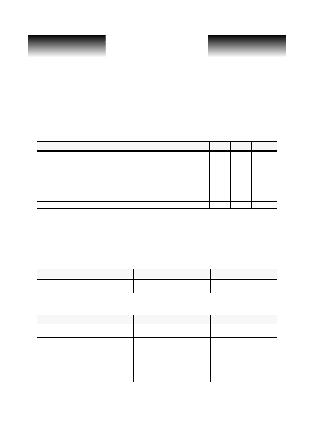
AC Timing Characteristics
The VSC6108/6110/6112 has an output time jitter of less than 25 ps peak-to-peak. To achieve this jitter
specification the input reference clock must have less than 10 ps peak-to-peak. Output skew is less than 50 ps
between any two outputs.
Table 3: AC Timing Specifications
DC Characteristics
The VSC6108/6110/6112 can be operated from a single 3.3-Volt power supply. Using a -3. 3-Volt supply,
the inputs and outputs are ECL-compatible. Using a +3.3-Volt power supply, the inputs and outputs are PECLcompatible. Total power dissipation is less than 2 Watts.
Table 4: Single Ended ECL Inputs
Note: VEE = -3.3V ± 5%, VCC = GND, Load = 50 to -2.0V , V
REF
= -1.32V ± 25 mV.
Table 5: Differential ECL Inputs and Outputs
Parameter Description Min Typ Max Units
RCd Reference clock duty cycle 40 60 %
RCj Reference clock jitter 10 pSPP
OCd Output clock duty cycle 40 60 %
OCj Output clock OCLK0-17 jitter 25 pSPP
T s k Skew between any ou tp ut clock to any other clock -50 +50 ps
Lr Reference Clock RCK/RCKN frequency range -1.0 +1.0 %
Lt Lock time 10
µS
t
rf
Output rise/fall time 20-80% 100 150 ps
Parameter Description Min Typ Max Units Conditions
V
IH
Input HIGH voltage -1020 - -700 mV
V
IL
Input LOW vol tage -2000 - -1620 mV
Paramet er Description Min Typ Max Units Cond itions
V
IN,DIFF
Input Voltage Differential 200 - - mV
Required input
voltage swing
V
IN,CM
Input Common Mode
Voltage
-1.5 - -0.5 V
Required input
common mode
voltage
V
OUT,DIFF
Output Voltage Differential 400 - 800 mV
Output voltage
swing
V
OUT,CM
Output Common Mode
Voltage
-1.6 - -1.2 V
Common mode
output voltage
 Loading...