

VITESSE SEMICONDUCTOR CORPORATION
Page 1
8/28/00 741 Calle Plano, Camarillo, CA 93012 • 805/388-3700 • FAX: 805/987-5896
VITESSE
SEMICONDUCTOR CORPORATION
Data Sheet
SC6048
G52335-0, Rev. 4.0
High-Speed Octal
Programmable Timing Generator
Features
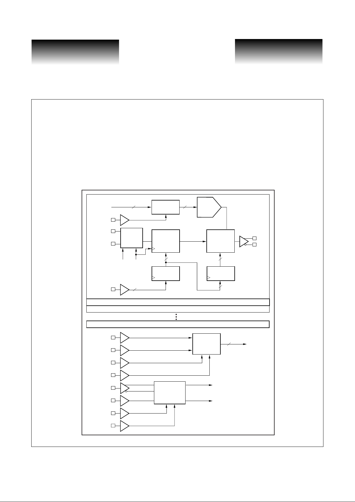
VSC6048 Block Diagram
• 100MHz/200MHz Dynamic Reprogram Frequency
for Incrementing and Decrementing
• Internal or External High-Speed Clock Option
• Low Power: 8 Watts, max
• Low Cost 160-Pin PQFP Packaging
• 8 Fully Integrated Timing Generators for ATE
Applications
• 10/5ns Delay Range, 10ps Resolution
• Fully Digital Interface. No Off-Chip DACs or
Trim Components Required
• ± 4 LSB Differential Non-Linearity
DAC_WR
CAL_DAT
Register
SPAN
CAL
DAC
IN0A
IN0B
DIN
TEST[0:9]
Register
Channel 1
Channel 0
Channel 2
Channel 7
Variable
Shift
Register
Input
Interleve
800MHz
Clock
400MHz
Clock
3
Vernier
Delay
Element
Out 0
Calibration
Register
400MHz Clock
800MHz Clock
PLL
Clock Multiplier
Unit
x8, x16
Register
7
7
10
6
CAL_DAT
6
6
ADR[0:2]
DCLK
SHIFT
RCK
RCKN
BYP
FSEL
PLLRST
VITESSE
SEMICONDUCTOR CORPORATION
Data Sheet
VSC6048
High-Speed Oct al
Programmable Timing Generator
Page 2
VITESSE SEMICONDUCTOR CORPORATION
741 Calle Plano, Camarillo, CA 93012 • 805/388-3700 • FAX: 805/987-5896 8/28/00
G52335-0,Rev.4.0
Functional Description
Reference Clock Selection
Clock multiplication of x8 or x16 may be selected via the FSEL pin, requiring a reference clock of 100
±2.5MHz or 50 ±1.25MHz, respectively. For system applications with 800MHz on board clock, the CMU can
be bypassed by asserting BYP signal and RCK will accept an external 800MHz clock.
In Bypass mode (BYP = 1, RCK = 800MHz) the skew from INX to RCK at the pin is 550ps +/-250ps.
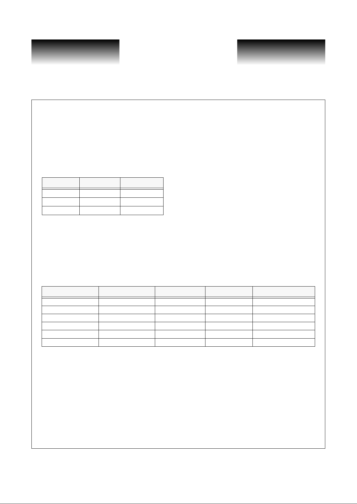
Ta ble 1: Reference Clock Selection
X = don’t care.
Mode of Operations
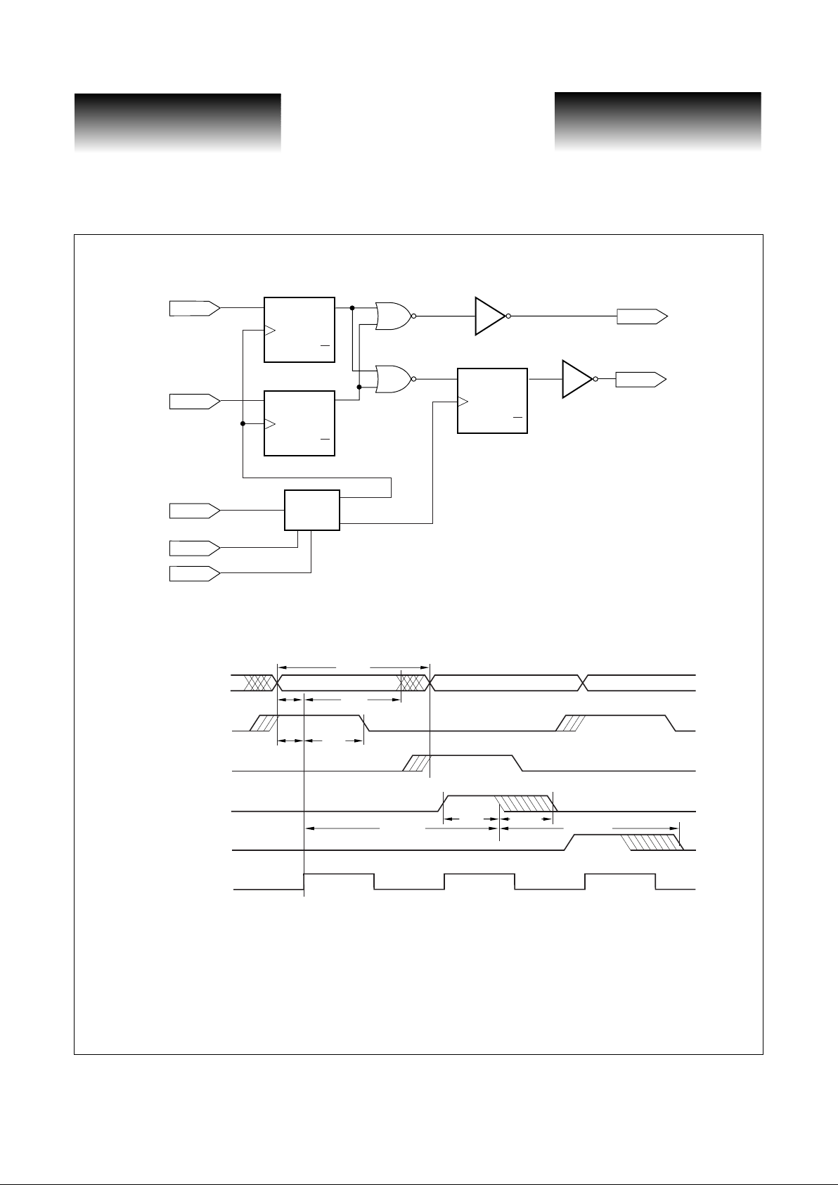
There are 6 basic modes of operatio n. These mod es are based on t wo input s per channel (INA a nd INB) t hat
can be interleaved and refire rate. The maximum refire rate for full 10ns span is 100MHz, where the maximum
refire rate for 5ns span is 200MHz. The maximum refire rate at the input to the fine vernier must not be sooner
than 4 cycles of the high-speed clock (800MHz).
T able 2: Suggested Operating Modes
Data Input (INA, INB)
There are two interleaved inputs per channel. Each input is capable of running at full rate (200MHz). The
input is first retimed off of the inte rnal 400MHz cl ock generate d from the PLL. This means t here is a 2.5ns edge
placement window that defines the setup time. This also means that the input pulse must span at least one
400MHz clock edge.
The inputs are low to high edge sensitive. Figure 1 illustrates an equivalent circuit of the input structure for
each channel. Note that the TSET input clock is generated based on the input data.
BYP FSEL RCK
0
0100MHz
0
150MHz
1
X800MHz
Program Rate Interleaved INA INB TSET[0:9] Range
200Mbps Yes 100MHz 100MHz 000 to 1FF
100Mbps Yes 50MHz 50MHz 000 to 3FF
200Mbps No 200MHz Low 000 to 1F F
100Mbps No 100MHz Low 000 to 3F F
200Mbps No Low 200MHz 000 to 1FF
100Mbps No Low 100MHz 000 to 3FF
VITESSE SEMICONDUCTOR CORPORATION
Page 3
8/28/00 741 Calle Plano, Camarillo, CA 93012 • 805/388-3700 • FAX: 805/987-5896
VITESSE
SEMICONDUCTOR CORPORATION
Data Sheet
SC6048
G52335-0, Rev. 4.0
High-Speed Octal
Programmable Timing Generator
Figure 1: Input Interleave
Figure 2: Functional Timing Diagram
Time Set Input (TSET<0:9>)
This is a 10-bit TTL bus that controls the delay value of the vernier. The 3 MSBs cont rol the 800MHz shift
register and the 7 LSBs control the fine delay element. The TSET data is clocked in by a pulse generated from
the input data. The setup time o f the TSET data is the same as the input signals (INA, INB). The TSET data
must be stable by the time the input edge arrives at the input pin and data m ust then be held stable for at leas t
3.5ns after the input edge arrives at the pin.
TSET_CLK
D
SET
CLR
Q
DQ
D
SET
CLR
Q
DQ
D
SET
PLL
CLR
400MHz
800MHz
Q
DQ
DATA
INxA
INxB
RCK
FSEL
BYP
t
RATETS
t
SETH
t
SETSU
IN
SU
t
OPW
t
PDV(SPAN)
t
PDTG(SPAN)
t
PDTG(MIN)
TSET[0:9]
INA
INB
RCK
OUT
TSET (0000000000)
OUT
TSET (1111111111)
IN
H

VITESSE
SEMICONDUCTOR CORPORATION
Data Sheet
VSC6048
High-Speed Oct al
Programmable Timing Generator
Page 4
VITESSE SEMICONDUCTOR CORPORATION
741 Calle Plano, Camarillo, CA 93012 • 805/388-3700 • FAX: 805/987-5896 8/28/00
G52335-0,Rev.4.0
Figure 3: Fine Vernier Calibration DAC Programming
DAC Calibration
Each fine vernier must be calibrated to a 1240ps span, one step (10ps) shorter than the 800MHz period
(1.25ns). This is accomplished by setting the fine vernier to maximum delay and adjusting the 6-bit calibration
DAC until the desired range has been achieved.
The calibration data is transferred into the device through a 3-bit serial interface. Refer to Figure 3 for the
programming sequence. Typical DCLK frequencies are 1MHz to 10MHz. Once the calibration value has been
transferred into the device, the data is written into the specified DAC by the r ising edge of DCLK when
DAC_WR is HIGH. The address lines must remain stable from the enable of SHIFT to one cycle after the disable of DAC_WR.
DAC Application
There are three DAC_REF pins on this device. Each pin supplies the reference for two or three calibration
DACs. In order to reduce crosstalk between verniers through the DAC_REF supply, it is recommended that
each DAC_REF pin be isolat ed from each other. This will reduce crosstalk b etween the the three channel
groups, however, it will not effect crosstalk between verniers within each group.
Table 3: DAC Reference Pin Identification
Outputs
Each channel has a differential ECL output. The output of the verniers is falling edge active. The shift reg-
ister propagates a 2ns pulse. The fine vernier then stretches the pulse width based on the programmed delay.
DAC_REF Pin # Vernier Channels
10, 1, 2
18 3, 4
40 5, 6, 7
SHIFT
DCLK
DIN
DAC_WR
CAL_DAT
(internal)
ADR[2:0]
543210
Vernier 0 DAC Data
XXXXX 543210XXXX
1
23456
1
23456
Address for Vernier 0
Vernier 1 DAC Data
Address for Vernier 1
Shift Data Into
Calibration Register
Hold Data In
Calibration Register
One T est/Calibration Cycle
VITESSE SEMICONDUCTOR CORPORATION
Page 5
8/28/00 741 Calle Plano, Camarillo, CA 93012 • 805/388-3700 • FAX: 805/987-5896
VITESSE
SEMICONDUCTOR CORPORATION
Data Sheet
SC6048
G52335-0, Rev. 4.0
High-Speed Octal
Programmable Timing Generator
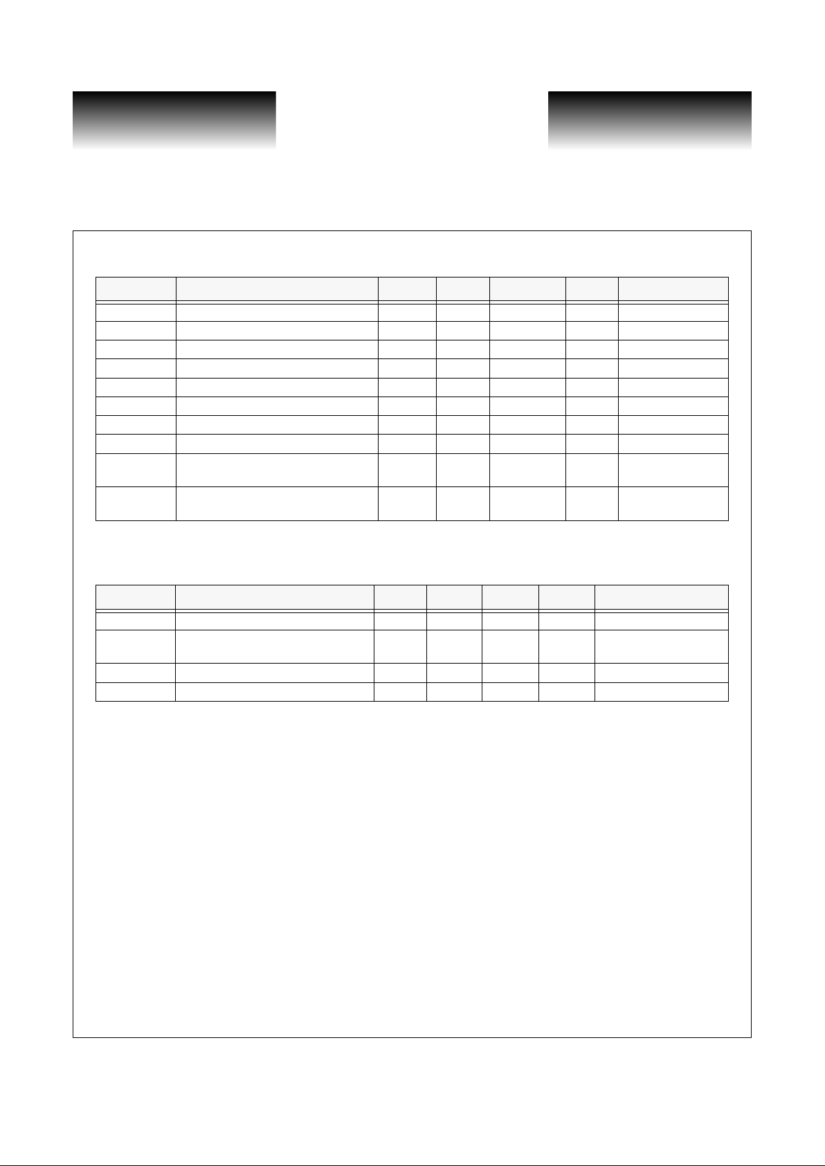
DC Characteristics
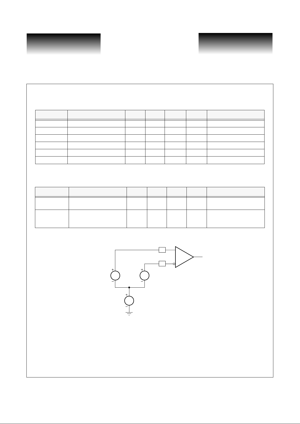
Table 4: Single Ended ECL Inputs and Outputs
NOTE: VTT = -2.0V ± 5%, VCC = V
CCA
= GND, R
LOAD
= 50Ω to -2.0V.
Table 5: Differential ECL Inputs and Outputs
Figure 4: Differential ECL Input Voltages
Parameter Description Min Typ Max Units Conditions
V
OH
Output HIGH Voltage -1020 - -700 mV
V
OL
Output LOW Voltage -2000 - -1620 mV
V
IH
Input HIGH Voltage -1165 - -700 mV
V
IL
Input LOW Voltage -2000 - -1475 mV
I
IH
Input HIGH Current - - 200 uA V
IN
= VIH (max)
I
IL
Input LOW Current -50 - - uA V
IN
= VIL (min)
Parameter Description Min Typ Max Units Conditions
V
DIFF
Input Voltage Differential 200 - - mV
Required for full output
swing
V
CM
Common-Mode Voltage -1.5 - -0.5 V
Common-mode range
required for full output swing
with V
DIFF
applied
V
DIFF
/2
V
CM
V
DIFF
/2
Pad
PadN
VITESSE
SEMICONDUCTOR CORPORATION
Data Sheet
VSC6048
High-Speed Oct al
Programmable Timing Generator
Page 6
VITESSE SEMICONDUCTOR CORPORATION
741 Calle Plano, Camarillo, CA 93012 • 805/388-3700 • FAX: 805/987-5896 8/28/00
G52335-0,Rev.4.0
Table 6: TTL Inputs and Outputs
NOTE: All specifications are over recommended commercial operating conditions, TTL/GND = GND.
Table 7: Power Supply Requirements
NOTE: (1) Output power dissipation does not include load power.
Parameter Description Min Typ Max Units Conditions
V
OH
Output HIGH Voltage 2.4 - - V I
OH
= -2.4mA
V
OL
Output LOW Voltage 0 - 0.4 V I
OL
= 16 mA
V
IH
Input HIGH Voltage 2.0 - V
TTL
+1.0V V -
V
IL
Input LOW Voltage 0 - 0.8 V -
I
IH
Input HIGH Current - - 50 µA V
IN
= 2.4V
I
IL
Input LOW Current -500 - - µA V
IN
= 0.4V
I
OZH
Tri-State Ou tp ut O FF Curren t HIGH - - 200 µA V
OUT
= 2.4V
I
OZL
Tri-State Output OFF Curre n t LOW -100 - - µA V
OUT
= 0.4V
I
OZLB
Tri-State Output OFF Current Low for
Bi-directs
-600 - - µA
V
OUT
= 0.4V
I
OCZ
Open Collector Output Leakage
Current
--200µA
V
OUT
= 2.4V
Parameter Description
Min
Typ Max Units Conditions
I
TT
Power Supply Current from V
TT
3.4 mA
I
DACREF
Power Supply Current from
V
DACREF
80 mA
I
TTL
Power Supply Current from V
TTL
250 mA
P
D
Power Dis sipation
(1)
8W
 Loading...