

VITESSE SSC055 Datasheet
.
VSC055
Enhanced I2C Backplane
Controller
Product Brief
Overview
The VSC055 Enhanced I2C Backplane Controller is
an integrated CMOS circuit that significantly
reduces system cost by integrating all of the digital
logic typically required to monitor a storage
enclosure. The VSC055 may be used in any
embedded control application including parallel
SCSI, Fibre Channel or any other application where
the monitoring and control of a large number of
digital I/O signals is required. Programming the
VSC055 is easy through a convenient programming
model, which reduces the overall duration of the
design-in cycle. Data is read and written to the
device over an addressable (3-bit) I2C serial
interface, allowing multiple VSC055 devices on a
single two-wire bus.
Device Features
• Up to 64 bits of user-definable, bi-directional
general purpose I/O (5 volt tolerant)
• Slave mode I2C serial interface
• Integrated Port Bypass, Clock Recovery and
Signal Detect support for up to 16 drives
• Eight programmable fan speed monitoring
inputs
• Eight programmable pulse width modulated fan
control outputs
• Pairing of GPI/O pins for direct input/output
signal routing/buffering
• Two clock input ranges: 8 to 10MHz (crystal) or
8.0 to 53.125MHz (oscillator)
• Automatic synchronization control between
multiple devices
• Selectable direct LED drive flashing capability
• Pin-programmable addressing for up to 16
devices on a single serial bus
• 100 PQFP Package
I2C Serial Interface
The VSC055 uses an I2C serial interface to
communicate with embedded controllers such as
Vitesse’s SSC100/200 and VSC205/210. The slave
interface on the VSC055 uses a three-bit (A2:0)
addressing scheme for identification on the serial
interface. The ASEL pin determines the four-bit
device type identifier. Up to sixteen, VSC055 or
SSC050 devices may reside on a single I2C
interface.
I/O Pins
The VSC055 has 64 bi-directional I/O pins. The
functionality of these pins is configurable via
programming of the VSC055. All I/O pins have a
12mA drive strength, support 3.3V TTL, and are 5V
tolerant. To enable the designer to configure and
program the VSC055, the 64 I/Os are arranged in
registers of eight pins. Certain groups of pins have
additional functionality beyond simple input or
output to support the integrated fan speed sensors,
PWM control, and FC-AL port bypass control.
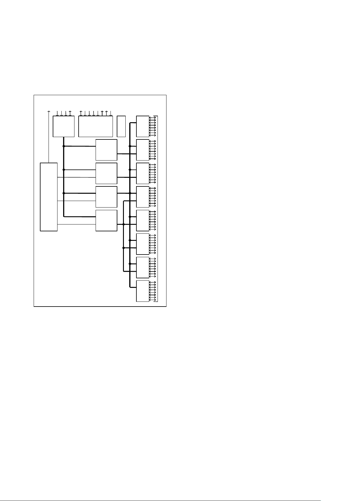
Drive Bay 1
Drive Bay 2
Drive Bay 3
Drive Bay 4
VSC7122
VITESSE
Enhanced Backplane
Controller
(VSC055)
Local I/O (x8)
VITESSE
Embedded
Controller
(SSC100)
Temperature
Sensor (LM75)
Flash
(64K x 8)
I2C Serial
Interface
PBC_EN1
PBC_EN2
PBC_EN3
PBC_EN4
Power Supplies
LEDs (x8)
PBC_EN
Fans (x4)
VSC7120
Cu or
Optics
X24C16
EEPROM
VSC7120
PBC_EN
Application for a Single Loop, Single Controller with Four Drives
.
LED Flash Rate Control
The built-in flexibility of the VSC055 allows all sixtyfour of the I/O pins to drive LEDs. Each pin is
independently programmed to flash an LED at one
of seven predefined flash rates or by firmware
definition.
Fan Speed Sensor
The VSC055 includes eight pins (P2.0 to P2.7),
which can be configured as fan speed sensors.
This feature enables the designer to provide high
value monitoring features at significantly reduced
costs. Embedded controllers may access the
VSC055 to determine the rotational speed (RPM) of
fans attached to each of the eight inputs. The
VSC055 may also be programmed to signal an
interrupt if any one of the speed sensors fall below
the designer’s predefined level.
Pulse Width Modulation Control
The VSC055 includes eight pins (P1.0 to P1.7),
which can be configured for three different pulse
rates with adjustable high/low duty cycle. This
feature enables the designer to control fan speed
via an external power MOSFET. Embedded
controllers may access the VSC055 to manage the
rotational speed (RPM) of fans attached to each of
the eight outputs.
FC-AL Port Bypass Control
Up to thirty-two of the sixty-four I/Os may be
configured to monitor and manage FC-AL port
bypass control devices. Sixteen pairs of I/Os
include special logic to monitor Enable Bypass
signals, which may be generated by FC-AL disk
drives, and control Port Bypass Control Enable
(PBC_Enx) signals on port bypass devices such as
Vitesse’s VSC7122.
The unique functionality of the VSC055 provides
the system designer with additional flexibility and
control over the port bypass function in a FC-AL
enclosure. This allows system designers to
differentiate and add value by controlling when and
how a drive is removed or inserted into a FC-AL
enclosure.
This feature may also be used for non-FC-AL
applications. It is useful wherever system
designers require flexible monitoring and control of
backplane signals.
Interrupt Support
There are up to sixty-four interrupt sources within
the VSC055. I/O pin signal transitions, fan speed
sensor threshold levels and transitions on port
bypass inputs may be configured to generate
interrupts. Advanced interrupt priority and
management logic provides the system designer
with maximum flexibility and a simple and
convenient programming method for handling
interrupts.
Related Documents
§ VSC055 Data Manual
§ SSC100/200/VSC205/210 Data Manual
§ Any SDK Specification
For More Information:
www.vitesse.com
email: prodinfo@vitesse.com
TEL: 1-800-VITESSE FAX: 805/987-5896
Vitesse Semiconductor Corporation reserves the right to make
changes in its products, specifications or other information at any
time without prior notice. Therefore the reader is cautioned to
confirm that this datasheet is current prior to placing any orders.
The company assumes no responsibility for any circuitry
described other than circuitry entirely embodied in a Vitesse
product. (Version 1.0)
© 2000 Vitesse Semiconductor Corporation, All Rights
Reserved.
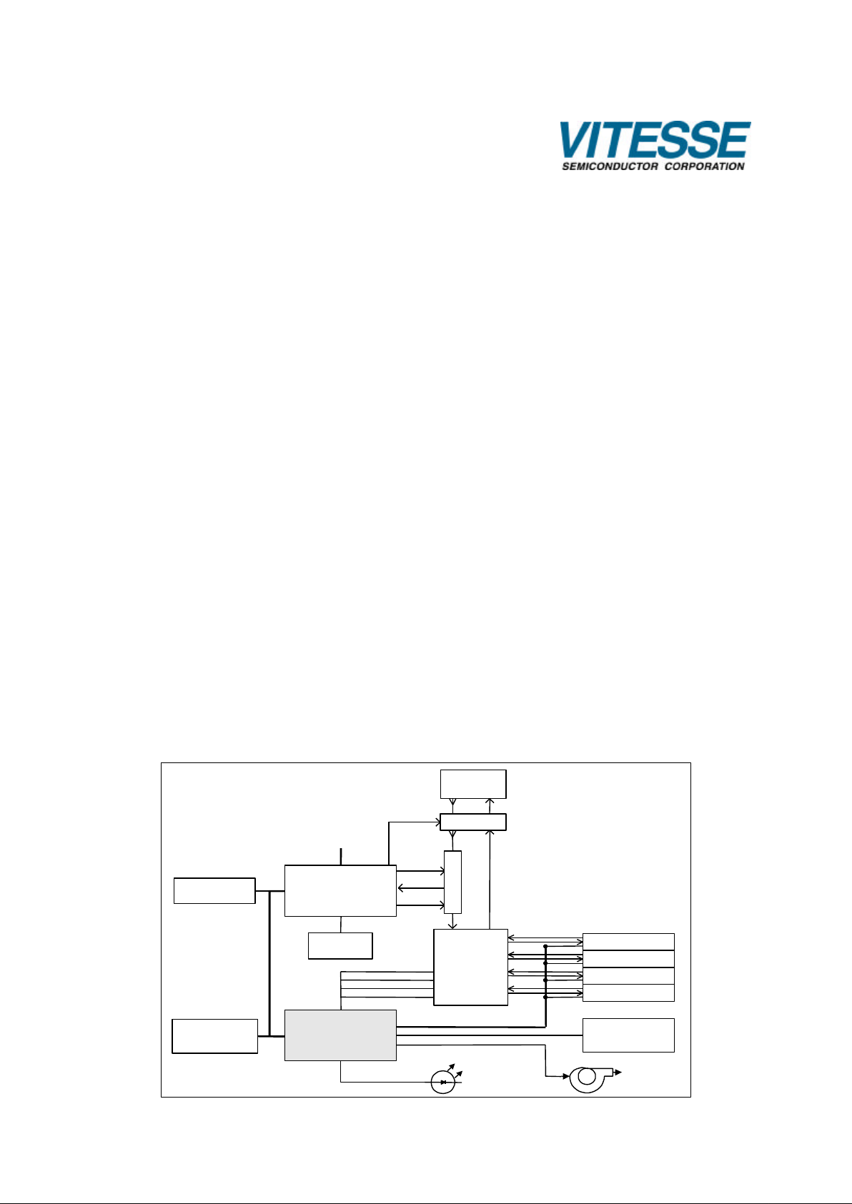
Two-Wire
Slave
Interface
Interrupt Priority and Control
Clock
Generator
and Dividers
I/O Ports
I/O Control
and LED
Flashing
P0.0 - P0.7 P1.0 - P1.7 P2.0 - P2.7 P3.0 - P3.7 P4.0 - P4.7
Fan Speed
Sensors
Port Bypass
Control
Power
On Reset
CKSEL0
CKOUT
SDA
SCL
A2-A0
ASEL
INT#
OSCI
OSCO
CKSEL1
P5.0 - P5.7 P6.0 - P6.7 P7.0 - P7.7
Pulse Width
Modulation
Control
SYNCEN
SYNC#
CKSEL2
VSC055 Block Diagram
 Loading...