


®
®
Vision
Components
The Smart Camera People
VCSBC4012
Operating Manual
Hardware specifications and special software functions of
VCSBC4012 Single Board Smart Cameras
Revision 2.0 April 2011
Document name: VCSBC4012.pdf
© Vision Components GmbH Ettlingen, Germany
VCSBC4012.pdf VCSBC4012 Single Board Smart Camera Operating Manual
2
Foreword and Disclaimer
This documentation has been prepared with most possible care. However Vision Components GmbH
does not take any liability for possible errors. In the interest of progress, Vision Components GmbH
reserves the right to perform technical changes without further notice.
Please notify
support@vision-components.com if you become aware of any errors in this manual or
if a certain topic requires more detailed documentation.
This manual is intended for information of Vision Component’s customers only. Any publication of this
document or parts thereof requires written permission by Vision Components GmbH.
Trademarks
Code Composer Studio and TMS320C6000, Windows XP, Total Commander, Tera Term, Motorola
are registered Trademarks. All trademarks are the property of their respective owners.
References
Since the VCSBC40XX smart camera family employs a TI processor, the programming environment
and functions for the VC20XX cameras can be used for this camera.
Please also consult the following resources for further reference:
“
Support News” for an overview of latest updates and support information
“
Knowledge Base / FAQ” for a searchable data base of SW and HW questions / answers
Description Title on Website Download Area
Quick start Manual for VC
camera set up and
programming
Getting Started VC Smart
Cameras with TI DSP
Public Download Area Getting Started
VC SDK Ti
Schnellstart VC – deutsche
Version of „Getting Started VC“.
Schnellstart VC Smart
Kameras
Customer Area Getting Started
VC20XX and VC40XX Cameras
Introduction to VC Smart Camera
programming
Programming Tutorial for
VC20XX and VC40XX
Cameras
Customer Area Getting Started
VC20XX and VC40XX Cameras
Demo programs and sample code
used in the Programming Tutorial
Tutorial_Code
Customer Area Getting Started
VC20XX and VC40XX Cameras
VC40XX Hardware Manual
VC40XX Smart Cameras
Hardware Documentation
Public Download Area Hardware
Documentation VC Smart Cameras
VCRT Operation System Functions
Manual
VCRT 5.0 Software Manual
Registered User Area Software
documentation VC Smart Cameras
VCRT Operation System TCP/IP
Functions Manual
VCRT 5.0 TCP/IP Manual
Registered User Area Software
documentation VC Smart Cameras
VCLIB 2.0 /3.0 Image Processing
Library Manual
VCLIB 2.0/ 3.0 Software
Manual
Registered User Area Software
documentation VC Smart Cameras
- The Light bulb highlights hints and ideas that may be helpful for a development.
- This warning sign alerts of possible pitfalls to avoid. Please pay careful attention
to sections marked with this sign.
!
Author: VC Support,
mailto:support@vision-comp.com
© 1996-2011 Vision Components GmbH Ettlingen, Germany

VCSBC4012.pdf – VCSBC4012 Single Board Smart Camera Operating Manual 3
Table of Contents
1 General Information 4
2 Basic Structure 5
3 Technical Specifications VCSBC4012 6
4 Camera Interfaces 7
4.1 J1: Power Supply and IO Interface 8
4.1.1 Pin Assignments J1 camera socket 8
4.1.2 Electrical specifications digital IO s J1 interface 8
4.1.3 Electrical specifications of the VCSBC4012 Power Supply J1 interface 10
4.2 J2: Expansion Port / Trigger Interface 11
4.2.1 Pin Assignments J2 camera socket 11
4.2.2 Matching connector and cable for J2 camera socket 12
4.2.3 Electrical specifications J2 camera socket 14
5 Accessories 16
5.1 Camera and Lens holder order numbers: 16
5.2 Further accessories available for the VCSBC4012: 16
6 Programming VCSBC4012 Camera 17
6.1 Special Software requirements for the VCSBC4012 17
6.2 Ethernet Communication 18
6.3 Using FTP with the VCSBC4012 18
6.4 Preventing Autoexec Execution / IP number reset 18
6.4.1 Resetting the Camera with help of the VCnet Recovery Tool 19
6.5 Special VCRT functions for programming VCSBC4012 cameras 20
6.5.1 Trigger Functions 20
6.5.2 Controlling the TTL IOs on socket J2 21
Appendix A: New VCRT Functions VCSBC4012 A
Appendix B: Drawing Circuit Board VCSBC4012 B
© 1996-2011 Vision Components GmbH Ettlingen, Germany
VCSBC4012.pdf – VCSBC4012 Single Board Smart Camera Operating Manual 4
1 General Information
VCSBC4012 Single Board Camera
The VCSBC4012 has been designed for high resolution image processing with a very small form
factor. The VCSBC4012 is the ideal compromise between high performance and low system costs,
and thus expecially suited for high volume OEM applications. This makes it viable to use a smart
camera in even more products than before.
Employing a CMOS sensor, the image resolution can be changed to the ROI required.
Like with all VC Smart Cameras with Texas Instruments DSP, the operation system VCRT allows
multi- tasking. This means for instance that user interface commands can execute in parallel without
stopping the inspection process. It is also possible to transfer live images via TCP/IP using a
background task.
The VCSBC4012 camera offers an inexpensive entrance into the world of the high performance
intelligent cameras. It has a video output onto a PC via 100MBit Ethernet interface, a high speed
trigger input and output, 12-24 V digital Inputs and open collector outputs and additional TTL IOs.
The extermely low power consumption of only 1.5W makes this camera ideally suitable for use in
mobile devices.
© 1996-2011 Vision Components GmbH Ettlingen, Germany
VCSBC4012.pdf – VCSBC4012 Single Board Smart Camera Operating Manual 5
2 Basic Structure
The image is formed by a high-resolution 5 mega pixel CMOS sensor. The image is then stored in
SDRAM memory, which has been increased to 64MB, due to the large camera image.
Unlike most other Vision Component Smart Cameras, the VCSBC4012 does not have a direct video
output. However if monitoring of the camera image is required, this can be done by downloading via
Fast Ethernet port to PC and display on screen (see
“Image Transfer” demo software under
“Support -> Customer Area -> Software Utilities”
).
The TMS320C64xx DSP is one of the fastest 32bit DSPs. It features a RISC-like instruction set, up to
8 instructions can be executed in parallel, two L1 cache memories (16 Kbytes each) and a 128 Kbytes
L2 cache on chip. Its high speed 64-channel DMA controller gives additional performance. The DSP
uses fast external SDRAM as main memory. A flash EPROM provides non-volatile memory.
Block diagram VCSBC4012 Camera
4 MB Flash
Eprom
CMOS
Sensor
Trigger In/
Out
Control/
Status Reg.
Open
collector IOs
64 MB SDRAM
TMS
C64XX
DSP
Bus Controller
Trigger In/ Out
24V In /
Open collector Out
Ethernet
Ethernet
10/100
© 1996-2011 Vision Components GmbH Ettlingen, Germany

VCSBC4012.pdf – VCSBC4012 Single Board Smart Camera Operating Manual 6
3 Technical Specifications VCSBC4012
Component / Feature Specification
CMOS Sensor: 1/ 2.5" Micron MT9P031 - also available with color sensor (Bayer Filter)
eff. no. of pixels: 2592(H) x 1944(V)
Pixel size: 2.2(H) x 2.2(V) µm
Chip size: 5.70(H) x 4.28(V) mm
High-speed shutter: “Electronic rolling shutter” (ERS) and “Global Reset Release” (GRR),
15µs, 45µs, 75 µs, … in steps of 30 µs
Low-speed shutter: up to 30 sec. adjustable integration time
Integration: ERS / GRR
Picture taking: program-controlled, full-frame / 11.6 frames per second, external high
speed trigger
Parallel image acquisition Not available
Clamping: Internal to sensor
A/D conversion: 80 MHz / 12 bit, only the 8 most significant bits used for grey values
Input LUT none
Image Display Via 100 Mbit Ethernet onto PC
Processor: Texas Instruments TMS320C64XX signal processor 400 MHz,
3200MIPS
RAM: 64 Mbytes SDRAM (synchronous dynamic RAM)
Memory capacity: Up to 13 full-size grey value images in format 2592 x 1944
Flash EPROM: 4 Mbytes flash EPROM (nonvolatile memory) for programs and data, in-
system programmable, 3 MB available to user
SD card: Not available
Process interface: 2 inputs / 4 outputs, outputs 4x80 mA
Additional LVTTL IOs: 4 Inputs, 4 Outputs, I2C Clock and Data signals (I2C also used internally
for Sensor control), trigger Input, Flash output
Ethernet interface: 10/100 Mbit
CE certification: No CE Certification from Vision Components as the OEM customer is
required to certify entire system (including housing, cabling, etc.).
Storage Conditions Temperature: -20 to 60 deg C, Max. humidity: 90%, non condensing.
Operating Conditions Temperature: 0… +55 deg C, Max. humidity: 80%, non condensing.
Power Supply 12V… 24V
Power Consumption ≈1.5W (current drawn from PLC outputs or onboard 3.3 V signal
additional)
© 1996-2011 Vision Components GmbH Ettlingen, Germany
VCSBC4012.pdf – VCSBC4012 Single Board Smart Camera Operating Manual 7
4 Camera Interfaces
J2
J3
J1
The VCSBC4012 camera board incorporates the following connector interfaces:
J 1 : VCSBC4012/ VCSBC50 Power and IO Connector
J 2: Ethernet, trigger and Expansion Port Connector
J 3: Emulator Connector
The pin assignments, electrical specifications as well as available accessories are sho wn for each
interface connector in the following sections.
Please refer to Please refer to “Appendix B: Drawing Circuit Board VCSBC4012” for the pin 1
orientation of the camera board sockets.
© 1996-2011 Vision Components GmbH Ettlingen, Germany
VCSBC4012.pdf – VCSBC4012 Single Board Smart Camera Operating Manual 8
4.1 J1: Power Supply and IO Interface
The J1 connector includes the camera power supply and the digital IOs.
4.1.1 Pin Assignments J1 camera socket
Pin Number Signal Core Color
1
1 Out0 Blue
2 Power (24V) Red
3 Out1 purple
4 Power GND Black
5 Out2 Grey/ red
6 In0 Green
7 Out3 Blue/ red
8 In1 Yellow
9 GND grey
10 GND white
11 N.C. pink
12 3.3V out brown
J1 Standard VCSBC4012 socket:
Molex: 8783212-20
Note that the pin allocation differs
from the J3 connector of the
VCSBC4018/16 board cameras!
Pin Locations
1 2
3 4
5 6
7 8
9 10
11 12
If board orientation as shown below:
Sensor
J1
4.1.2 Electrical specifications digital IO s J1 interface
The camera has two PLC compatible inputs and four PLC compatible open-collector outputs for
controlling machines and processes.
Inputs and outputs are not galvanically separated from the supply voltage.
!
A protective diode ensures, the poles of the supply voltage from the power supply of the PLC can not
be swapped.
The outputs are floating when high – external pull up resistor required.
1
According to matching Power / PLC Cable VK000173
© 1996-2011 Vision Components GmbH Ettlingen, Germany

VCSBC4012.pdf – VCSBC4012 Single Board Smart Camera Operating Manual 9
Input Signals IO interface
Nominal voltage: 12 – 24 V
Absolute maximum voltage: voltages greater than 40 V can destroy the inputs
Type: Circuit GND directly connected
Input current: 1 mA @ 24V
Threshold value: 10 V
Internal signal delay: - No delay for direct IO access
- 10ms delay for DSP polling
The PLC-compatible inputs (24-V level, the positive signal is detected) include input protection circuits.
A minimum voltage of 10V is required to reliably sense a logic high signal.
Output Signals IO Interface
Operating voltage: Depends on external output supply
Absolute maximum voltage: voltages greater than 40 V can destroy the outputs
Type: BC850 open collector
Switching voltage: negative switching (NPN), output high switching to GND
Current: max. 80 mA per output
Absolute maximum current:
total currents greater than 80 mA per output can destroy
plugs and cables
no inductive/ capacitive load allowed
Switching power: max. 1.0 W per output
Protection against inductive
loads:
no
Resistance when switched on: 20 Ohm
Short circuit protection: No protection
Suggested external circuit for using camera outputs NPN
GND
R pull- up, 1k – 10k,
depending on Voltage
(5V: 1k – 24V: 10k)
Camera output circuit
(internal)
External output circuit
external supply
Output signal voltage
output transistor
switching to GND
© 1996-2011 Vision Components GmbH Ettlingen, Germany

VCSBC4012.pdf – VCSBC4012 Single Board Smart Camera Operating Manual 10
4.1.3 Electrical specifications of the VCSBC4012 Power Supply J1 interface
Nominal Voltage: 12V – 24V
Nominal Power Consumption2: 1.5W
Minimum operational voltage (including ripple): 9V
Minimum nominal Operating voltage and
corresponding current:
12V
116mA
3
Maximum nominal Operating voltage and
corresponding current:
24V
70mA
3
Maximum operational Voltage (including ripple): 30V
Power must be connected to the 12 pin J1 I/O connector.
Camera power is regulated, so only an unregulated power source of 12 V to 24V is required. The
camera is, however, very sensitive to power supply interruption. Please make sure, that the voltage
never exceeds the limits of < 9V, > 30V even for a short period of time. In case of trouble it is
recommended to backup the power supply by a capacitor or a battery large enough to prevent power
interruptions.
Power consumption depending on suply voltage
3
:
Supply
Voltage
[V]
Current
drawn
[mA]
Power
3
Consumption
[W]
9 153 1.37
10 138 1.38
12 116 1.39
14 100 1.40
16 90 1.44
18 80 1.44
20 72 1.44
22 66 1.45
24 62 1.48
26 57 1.48
28 54 1.51
30 51 1.53
2
Typical power consumption without using the onboard 3.3V supply.
3
Current drawn from the 3.3V on board signal needs to be added to these figures.
© 1996-2011 Vision Components GmbH Ettlingen, Germany

VCSBC4012.pdf – VCSBC4012 Single Board Smart Camera Operating Manual 11
4.2 J2: Expansion Port / Trigger Interface
Note that the LVTTL IOs are very sensitive. Only use driving electronics suitable for LVTTL IO’s!
4.2.1 Pin Assignments J2 camera socket
Pin Number Signal
1
I2C_Clock
2
I2C_Data
3
Trig_in
4
Trig_out
5
Q00
6
I01
7
Q01
8
I01
9
Q02
10
I02
11
Q03
12
I03
Core Colors Ethernet
13
TxD+ Blue
14
TxD- Red
15
GND N.C.
16
GND N.C.
17
RxD+ Pink / black
18
RxD- Green
19
GND N.C.
20 GND N.C.
Cable colors shown valid for using VC’s Ethernet cables – see the accessory overview in section 5.
Signal description:
Q00 – Q03 digital LVTTL outputs
I00 – I03: Digital LVTTL input (without pull-up resistor)
I2C_Clock and I2C_Data I2C serial Bus Interface for additional peripherals (Refer to the Texas
Instruments documentation
4
for further details)
Note that the I2C Bus is used internally to program the sensor!
Caution is advised when programming the I2C in order not to block
system tasks!
Trig_in and
Trig_out
Trig_in and Trig_out – are not opto isolated, so special care must be
taken or Isolation has to be done externally!
4
“TMS320C6000 DSP Inter-Integrated Circuit (I2C) Module Reference Guide”, Literature Number:
SPRU175A, Oct. 2002
© 1996-2011 Vision Components GmbH Ettlingen, Germany

VCSBC4012.pdf – VCSBC4012 Single Board Smart Camera Operating Manual 12
Pin Locations
1 2
3 4
5 6
7 8
9 10
11 12
top part of J2 interface for I2C Bus, Trigger Interface and additional LVTTL
13 14
15 16
17 18
19 20
lower part of socket for Ethernet
Please refer to “Appendix B: Drawing Circuit Board VCSBC4012” for the pin 1 orientation on the
camera board socket.
4.2.2 Matching connector and cable for J2 camera socket
4.2.2.1 Manufacture own cable / pcb that sits on top of camera board
The socket J2 has the following part number: 8775967-2050, manufacturer Molex (
www.molex.com)
The matching connector has the following part number: 51110-2050
Vision Components does not currently manufacture a cable for this connector. Please order the
matching connector from the manufacturer Molex.
4.2.2.2 Using VC’s wide Ribbon Cable covering J1 and J2
There is a new Ribbon Cable available using a 24 pin Molex conector that connects to all 12 J1 and
20 J2 pins. This cable can be ordered with one connector / open and 2 female molex connectors.
For further details please contact sales at this stage:
sales@vision-comp.com .
© 1996-2011 Vision Components GmbH Ettlingen, Germany

VCSBC4012.pdf – VCSBC4012 Single Board Smart Camera Operating Manual 13
4.2.2.3 Use Power and Ethernet cable side by side
Alternatively an additional 12 pin Power Supply /PLC and a 8 pin Ethernet cable (Cable set for
VCSBC4018, VK000229 see section 5) can be used next to each other to cover all contacts. Since
only pin 1,2,5 and 6 of the 8 pin Ethernet connector are connected, place these two plugs on the J2
sockets as shown below:
Pin 1-12 use J1 cable Pin 13-20 use one of the Ethernet calbes, (pin number of connector given
here):
2 4 6 8 10 12 2 NC 6 NC
1 3 5 7 9 11 1 NC 5 NC
∇
Please refer to section 4.1.1, section 4.2.1 and sectio 5 for details on these cables.
Pin assignment Ethernet cable VK000251:
PIN (J4) Cable Color (J4) Signal Cable Color (RJ45) PIN (RJ45)
1 blue TXD+ Orange/ white 1
2 red TXD- Orange 2
3 N/C GND N/C
4 N/C GND N/C
5 Pink / black RXD+ Green/ white 3
6 green RXD- Green 6
7 N/C GND N/C
8 N/C GND N/C
The change of core colors results from connecting two cables (VK000206 and a standard
Ethernet cat 5 cable).
© 1996-2011 Vision Components GmbH Ettlingen, Germany

VCSBC4012.pdf – VCSBC4012 Single Board Smart Camera Operating Manual 14
4.2.3 Electrical specifications J2 camera socket
All Signals are Low Level TTL (3.3V), not opto isolated.
The electrical specifications given for the trigger input and output are also valid for the remaining
LVTTL IOs.
The following Signals have a 1k5 pull up resistor on board:
-
I2C_Clock
- I2C_Data
- Trig_in
Trigger IO Specifications:
The board features a dedicated fast TTL trigger input (for use as image capture trigger) and a fast TTL
trigger output (as strobe-light trigger). Since both signals are fast at a very low noise margin, it is
recommended to keep the cable as short as possible. Use twisted pair or even coaxial cable for this
purpose. The trigger input assures a constant image capture delay without jitter.
Electrical Specification of trigger input
5
:
input voltage: Signal LOW -0.3V – 0.8V (LVTTL)
Input voltage: Signal HIGH 2V – 3.9V (LVTTL)
input current: N/A
limiting resistor: 1K5 pull up
reverse voltage protection: none
switching delay: none
Image trigger on rising or falling input signal works as before – see section 6.5.1 for details.
The trigger input and output are very sensitive and not galvanically separated. Opto
isolation of the driving circuit is therefore strongly recommended. The following page
shows suitable circuits for trigger input and output.
!
Please note that input and output are not protected against over current. The output is neither
protected against short circuit nor reverse voltage spikes from inductive loads.
Use the VC4018 or VC4016 cameras if you can not provide a suitable trigger input driving
circuit. These cameras include the same hardware as the VCSBC4018 / -16, but opto isolation
of the trigger input and output is already included.
5
The electrical specifications given for the trigger input and output are also valid for the
remainingLVTTL IOs.
© 1996-2011 Vision Components GmbH Ettlingen, Germany

VCSBC4012.pdf – VCSBC4012 Single Board Smart Camera Operating Manual 15
Recommended driving circuit for the trigger input:
Camera side:
Pin 15 Trig In
Electrical Specification of trigger output
6
:
output voltage signal LOW: 0.4 V with 2mA output current
0.2 V with 1mA output current
output voltage signal HIGH: 2.9 V with 8mA output current
3.1 V with 1mA output current max. 3 V LVTTL
Maximum output current: max. 8 mA (high), 2mA (low)
pull-up resistor: none, LVTTL push-pull output
Caution: Place the connectors at the correct position – not reversed or shifted.
Recommended circuit for trigger output:
Camera side:
Pin 16 Trig Out
6
The electrical specifications given for the trigger input and output are also valid for the
remainingLVTTL IOs.
© 1996-2011 Vision Components GmbH Ettlingen, Germany

VCSBC4012.pdf – VCSBC4012 Single Board Smart Camera Operating Manual 16
5 Accessories
For interface cables and connectors available also consult the corresponding section in chapter 4 of
this manual.
5.1 Camera and Lens holder order numbers:
Product / Service description Order Number
VCSBC4012 Single Board Smart Camera without lens holder, b/w CCD VK000368
VCSBC4012 Single Board Smart Camera without lens holder, Bayer CCD VK000369
Lens holder C Mount incl. adjustment (IR Filter EK000625 included) VK
Lens holder 12mm (Clear glass window EK000624 included) VK
5.2 Further accessories available for the VCSBC4012:
Product description Order Number
Power adapter for rail mounting, Input Voltage 100 – 240VAC 50/60 Hz
Output Voltage DC 24V +/-5%, max. 300 mA (7.5 W)
Equipped with connecting clamps for AC input and 24V output, CE cert.
Using this power supply with VCSBC4018 and VCSBC4016 is only
possible when booting by switching the 24V secondary side! 15W
power supply needed if switching the mains supply!
VK000036
Cable for Expansion Port J2 (use cable set VK000229 see section 4.2) It is
recommended to manufacture matching circuit board
VK000229
Power Supply and IO Interface cable for J1 VK000173
Ethernet OEM Cable for J2 (0.5m length, 4 single cores) VK000206
Ethernet testing Cable for J2 (2.5m length, other end with RJ45 connector) VK000251
Emulator Adaptor Cable for J3 VK
Cable set for VCSBC4012 (contains VK000206 and VK000173) VK000229
Cable for Emulator interface J3 VK
Clear glass protective sensor window (replaces IR filter in camera head) EK000624
IR cut filter (camera is shipped with this filter mounted) refer to Appendix B EK000625
!
All cable lengths are 0.5m unless stated otherwise.
Please also refer to the VC website
www.vision-components.com for an up to date list of
accessories.
© 1996-2011 Vision Components GmbH Ettlingen, Germany

VCSBC4012.pdf – VCSBC4012 Single Board Smart Camera Operating Manual 17
6 Programming VCSBC4012 Camera
The VCSBC4012 operating system includes some additional functions, mainly for the control of the
additional interfaces. Without direct VGA output some video control functions are not implemented for
this camera.
This manual describes the differences between the standard VCRT 5 operating system functions and
the special function library of the VCSBC40. For programming please also consult the
VCRT 5 and
VCLIB 2.0 and VCLIB 3.0 manuals (see the list of references at the beginning of this manual).
6.1 Special Software requirements for the VCSBC4012
The following table shows the minimum compatible setup options using the VCSBC4012 camera:
Code Composer Studio
Version
VCRT PC Lib Version VCLIB Version VCRT Camera OS
Version:
CCS 3.1 (C6000) or
CCS 3.3 (C6000)
VCRT 5.27 VCLIB 3.0 VCRT 5.27
Refer to the “Support News” section, under “Support and Download” on the VC website for an
overview of the latest compatible set up.
The VCRT PC lib Operation System PC library, the VCLIB Image Processing Library as well as the
VCRT Camera Operation System can be downloaded from Support section of the Vision Components
Website.
Software manuals are located in the “Registered User Area”. This download area can be a ccessed
after registration and log in on the VC Website.
Software updates are available from the “Customer Area”. For access to the customer area please
register your Vision Components development software for VC cameras with TI processor. Software
registration can be done after logging in using the license key code shipped with each development
bundle. For this please follow the “Register your Software” link under the “User Menu”.
© 1996-2011 Vision Components GmbH Ettlingen, Germany

VCSBC4012.pdf – VCSBC4012 Single Board Smart Camera Operating Manual 18
6.2 Ethernet Communication
The default camera IP address is 192.168.0.65 – as with all Ethernet cameras from VC.
The IP address can be changed to a different loading a #IP file into camera memory.
Refer to the “Getting Started VC Smart Cameras” guide for further details.
The camera supports DHCP server IP address allocation. In order to use DHCP allocation, the entry
“DHCP” needs to be added to the #IP file as shown:
DHCP
IP: 192.168.0.81
MSK: 255.255.255.0
GTW: 192.168.0.1
The camera uses the specified IP address if DHCP allocation is not successful. If no IP address is
specified in the #IP file, the camera falls back to the default address:
192.168.0.65
Please use DHCP server functions to determine the IP address allocated to the camera. Most
server show a list of mac addresses and corresponding IP addresses or allow to allocate fixed
IP addresses to a certain mac address. Determine the mac address of the camera using the
shell command “type #ID” to prior to using DHCP IP address allocation!
The “Getting Started VC Smart Cameras” and section 6.4.1 include advice on re-setting a camera with
unknown or invalid IP Address.
6.3 Using FTP with the VCSBC4012
With VCRT 5.18 and higher, the use of any standard ftp client is now possible. The following server
commands have been added: SYSTEM,PWD,CWD,LIST,DEL
Programs have to be uploaded as “out” files into the camera flash memory. Ascii files like the
autoexec or #IP files can be uploaded as “*.txt” files – the conversion into *.msf” files is not required.
6.4 Preventing Autoexec Execution / IP number reset
Preventing the execution of an Autoexec file by attempting a connection with the camera (as
described in the programming tutorial) does not work, due to the increased proc essor speed.
Resetting the camera using a keypad as with the VC20XX cameras is also not possible.
There are three ways of preventing the Autoexec execution and resetting the IP address:
Option 1:
1. Upload an empty autoexec/ #IP file via FTP into the camera memory, overwriting the existing
file(s).
2. Hardware reset of camera.
Option 2: CPU reset with help of an Emulator.
Option 3: Resetting the camera with help of the “VCnet Recovery Tool” as described in the following
section.
© 1996-2011 Vision Components GmbH Ettlingen, Germany

VCSBC4012.pdf – VCSBC4012 Single Board Smart Camera Operating Manual 19
6.4.1 Resetting the Camera with help of the VCnet Recovery Tool
A new tool – the “Vcnet Recovery Tool” is provided for resetting the IP address of the VCSBC4012
and VC4012 cameras. Vcnet Recovery is supported from camera OS VCRT 5.21.
In order to use the VCnet Recovery tool, follow the steps below:
1. Download and install the “
Java(TM) 2 Runtime Environment, Standard Edition 1.4.XX” on
your PC (Download from
www.sun.com - > Downloads - > J2SE v 1.4.2_11 JRE ).
2. Download VCnet Recovery Tool for VC4012 and VCSBC4012 from www.vision–
comp.com -> Support ->
Customer Area Software Utilities
3. Unpack the “vcnet1.2.zip” folder a directory on your hard drive (for instance C:\ti\Util…).
4. Open the Dos command line window and change to the directory containing “vcnet.jar”.
5. Execute the following command from the DOS Window "java -jar vcnet.jar -snr 5912345" , by
specifying the camera serial number as shown. This command sends vcp packets via UDP
broadcast for the next 15 seconds. Sending this command resets the corresponding camera
to the default IP address and bypasses Autoexec execution. Further options below.
6. Boot the corresponding camera (power on) during the next 15 seconds. During start up the
camera listens 0.5 seconds for cvp pac ket s send with vcnet.jar.
7. If a valid vcp packet is received from camera an answer packet is sent (see example below).
The camera continues booting in standard configuration:
Default IP address: 192.168.0.65
Mask: 255.255.255.0
Gateway: none
An autoexec in flash memory is not executed.
Example of resetting a VCSBC4012, S/N 0100151:
C:\Programme\VCnet>java -jar vcnet.jar -snr 0100151
VCnet Recovering Tool Version 1.2 - Copyright Vision Components 2005
Recovering Serial Number = 100151
Listening on port 67 for incoming packets!
Packet 2 from: /0.0.0.0
===Data as Text:===
model: VC4018E
S/N: 0100151
DC: 06/10/05 09:23:06
MAC: 00-06-1F-01-87-37
IP: 192.168.0.81
MSK: 255.255.255.0
GTW: 192.168.0.1
….
© 1996-2011 Vision Components GmbH Ettlingen, Germany

VCSBC4012.pdf – VCSBC4012 Single Board Smart Camera Operating Manual 20
6.5 Special VCRT functions for programming VCSBC4012 cameras
This sections explains the
specifics of programming VCSBC4012 cameras.
6.5.1 Trigger Functions
Apart form the inverse TTL logic (see section 4.2.3) and the different status register shown below, the
trigger works like with the VC4XXX cameras.
Please refer to the VCRT5.pdf manual – available form the Registered User Area of the VC website.
To query the trigger input, use the following command (see demo program trigin.c):
…
if (TRIGINP_PIN)
print("external trigger = 1\n");
else
print("external trigger = 0\n");
…
A capture can be triggered on rising edge with TRIGINP_POS() and on falling edge with
TRIGINP_NEG().
Signal Trigger Mode
TRIGINP_POS()
Rising Edge Trigger Signal
TRIGINP_NEG()
Falling Edge Trigger Signal
Trigger input
t
V
Threshold
Trigger input
t
V
Threshold
The trigger output can be set to exposure controlled mode – for instance to control a light source. With
TRIGOUT_EXP() combined with TRIGOUT_POS(), the trigger output is high during expo sure.
TRIGOUT_EXP() combined with TRIGOUT_NEG(), the trigger output is low during exposure.
© 1996-2011 Vision Components GmbH Ettlingen, Germany

VCSBC4012.pdf – VCSBC4012 Single Board Smart Camera Operating Manual 21
Trigger Output Signal in Exposure Controlled
Mode:
TRIGOUT_EXP();
AND
Trigger output set positive:
TRIGOUT_POS();
t
V
Trigger Output
The trigger macros are also described in our programming tutorial.
!
The use of TRIGOUT_USR(), SET_TRIGOUT() and RES_TRIGOUT() is limited on the VCSBC4012
camera! Use only with slow applications and long shutter times (the sensor needs several
milliseconds to execute the signal change).
6.5.2 Controlling the TTL IOs on socket J2
Setting and reading the 4LVTTL inputs and outputs is done with help of the hardware registers.
The following macros are available for easier operation (see “vcrt.h”):
- Setting the 4 outputs is done with help of a 4 bit value:
#define TTL_OUT(x) *((volatile int *)FA40_LED) = x /* SBC4018 TTL output */
- For queering the TTL inputs use the following function:
#define GET_TTL_IN() (*((volatile int *)FA40_TTL) & 0x0F) /* SBC4018 TTL input */
© 1996-2011 Vision Components GmbH Ettlingen, Germany

VCSBC4012.pdf VCSBC4012 Single Board Smart Camera Operating Manual
A
Appendix A: New VCRT Functions VCSBC4012
New VCRT functions (see section 6 and vcrt.h):
#define GET_HW_STATUS() (*((volatile int *)FA40_STATUS) & 0x3F) /* CPLD relase number*/
#define TTL_OUT(x) *((volatile int *)FA40_LED) = x /* SBC4012 TTL output*/
#define GET_TTL_IN() (*((volatile int *)FA40_TTL) & 0x0F) /* SBC4012 TTL input*/
© 1996-2011 Vision Components GmbH Ettlingen, Germany

VCSBC40XX.pdf – VCSBC4012 Single Board Smart Camera Operating Manual B
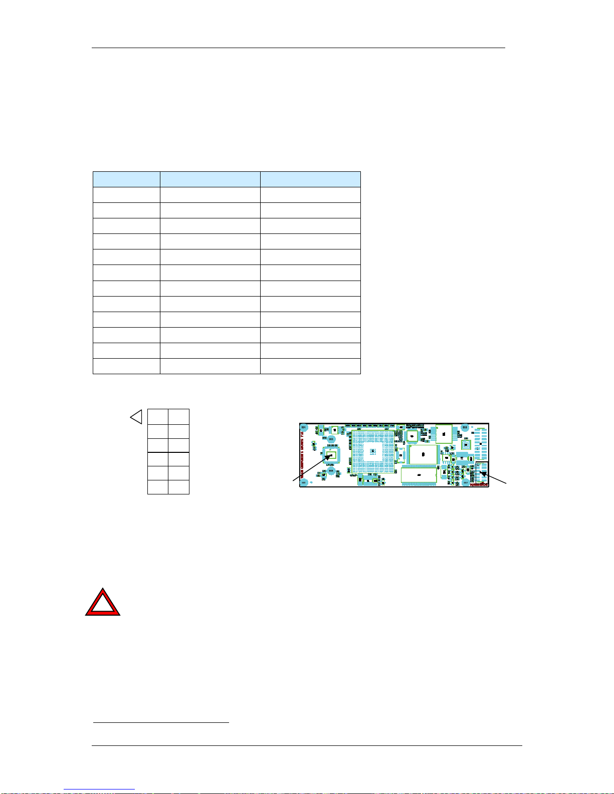
Appendix B: Drawing Circuit Board VCSBC4012
The red dot marks the Pin 1 position of each connector.
Correct placement
Of Emulator adapter
board
All mounting holes:
∅ 2.2mm for M2
Tolerances: All circuit board dimensions: +/- 0.1mm
© 1996-2011 Vision Components GmbH Ettlingen, Germany

C
Visit the Vision Components site www.vision-components.com for further information,
documentation and software downloads:
Web Site Menu Links Content
Contact
Distributor list / Enquiry forms
Home
Latest News from VC
Our Company
VC Company Information
News and Events
Trade Show dates
VC Publications
Sign in for free VC Seminars
VC Network
Description of Partner Companies
Application Overview
3
rd
Party Hard- and SW Products for VC Smart
Cameras
Products
VC Smart Camera Overview
Product Overview:
VC44XX VC Optimum
VC40XX VC Professional Family
VC4016 / 18 VC Base Family
VC4002L Line Scan Camera
VCSBC Single Board Cameras
VC20XX Smart Cameras
VCSBC Board Cameras
VCM + Viscube Camera Sensors
VC Smart Camera Software
VC Software Development Kit Ti: VCRT Operating System
VCLIB Image Processing Library
VC Special Libraries: M200 Data Matrix Code Reader
VCOCR Text Recognition Library
Color Lib
Support:
Support News (User Registration required) Tech News – new SW and Documentation
Knowledge Base / FAQ (User Registration
required)
Searchable FAQ Database with programming
Examples and Demo Code
Download Area Download of:
Public Download Area
(free Access)
- Product Brochures
- Camera Operat ing Manuals
Registered User Area
(User Registration required)
- Getting Started
- Programming Manuals
- Tr aining Manuals and Demo Code
Customer Download Area
(User- and SW License
Registration required)
- Software Updates (Libs and camera OS)
- Demo Code
- Utility Software
RMA Number Form Form for Allocation of Repair Numbers.
 Loading...