Vishay Telefunken BPW17N Datasheet

Silicon NPN Phototransistor
Description
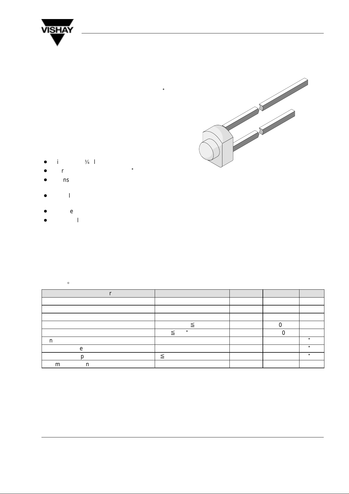
BPW17N is a silicon NPN epitaxial planar phototransistor in a miniature plastic case with a ± 12° lens.
With a lead center to center spacing of 2.54mm and a
package width of 2.4mm the devices are easily stackable on PC boards and assembled to arrays of
unlimited size.
Due to its waterclear epoxy the device is sensitive to
visible and near infrared radiation.
Features
D
Miniature T–¾ clear plastic package with lens
D
Narrow viewing angle ϕ = ± 12
D
Insensitive against background light due to narrow aperture
D
Suitable for 0.1” (2.54 mm) center to center spacing
D
Suitable for visible and near infrared radiation
D
Compatible with IR diode CQY37N
°
BPW17N
Vishay Telefunken
94 8639
Applications
Detector in electronic control and drive circuits
Absolute Maximum Ratings
T
= 25_C
amb
Parameter Test Conditions Symbol Value Unit
Collector Emitter Voltage V
Emitter Collector Voltage V
Collector Current I
Peak Collector Current
Total Power Dissipation
Junction Temperature T
Storage Temperature Range T
Soldering Temperature
Thermal Resistance Junction/Ambient R
tp/T = 0.5, tp x 10 ms
T
x 55 °C
amb
t x 3 s
CEO
ECO
C
I
CM
P
tot
stg
T
sd
thJA
32 V
5 V
50 mA
100 mA
100 mW
j
100
–55...+100
260
450 K/W
°
C
°
C
°
C
Document Number 81516
Rev. 2, 20-May-99
www.vishay.de • FaxBack +1-408-970-5600
1 (5)

BPW17N
Vishay Telefunken
Basic Characteristics
T
= 25_C
amb
Parameter Test Conditions Symbol Min Typ Max Unit
Collector Emitter Breakdown
Voltage
Collector Dark Current VCE = 20 V, E = 0 I
Collector Emitter Capacitance VCE = 5 V, f = 1 MHz, E = 0 C
Collector Light Current Ee = 1 mW/cm2,
Angle of Half Sensitivity ϕ ±12 deg
Wavelength of Peak Sensitivity
Range of Spectral Bandwidth
Collector Emitter Saturation
Voltage
Turn–On Time VS = 5 V, IC = 5 mA,
Turn–Off Time VS = 5 V, IC = 5 mA,
Cut–Off Frequency VS = 5 V, IC = 5 mA,
IC = 1 mA V
l
= 950 nm, VCE = 5 V
Ee = 1 mW/cm2,
l
= 950 nm, IC = 0.1 mA
RL = 100
RL = 100
R
= 100
L
W
W
W
(BR)CE
O
CEO
CEO
I
ca
l
p
l
0.5
V
CEsat
t
on
t
off
f
c
32 V
1 200 nA
8 pF
0.5 1.0 mA
825 nm
620...960 nm
0.3 V
4.8
5.0
m
m
120 kHz
s
s
Typical Characteristics (T
125
100
75
50
25
tot
P – Total Power Dissipation ( mW )
0
020406080
T
94 8308
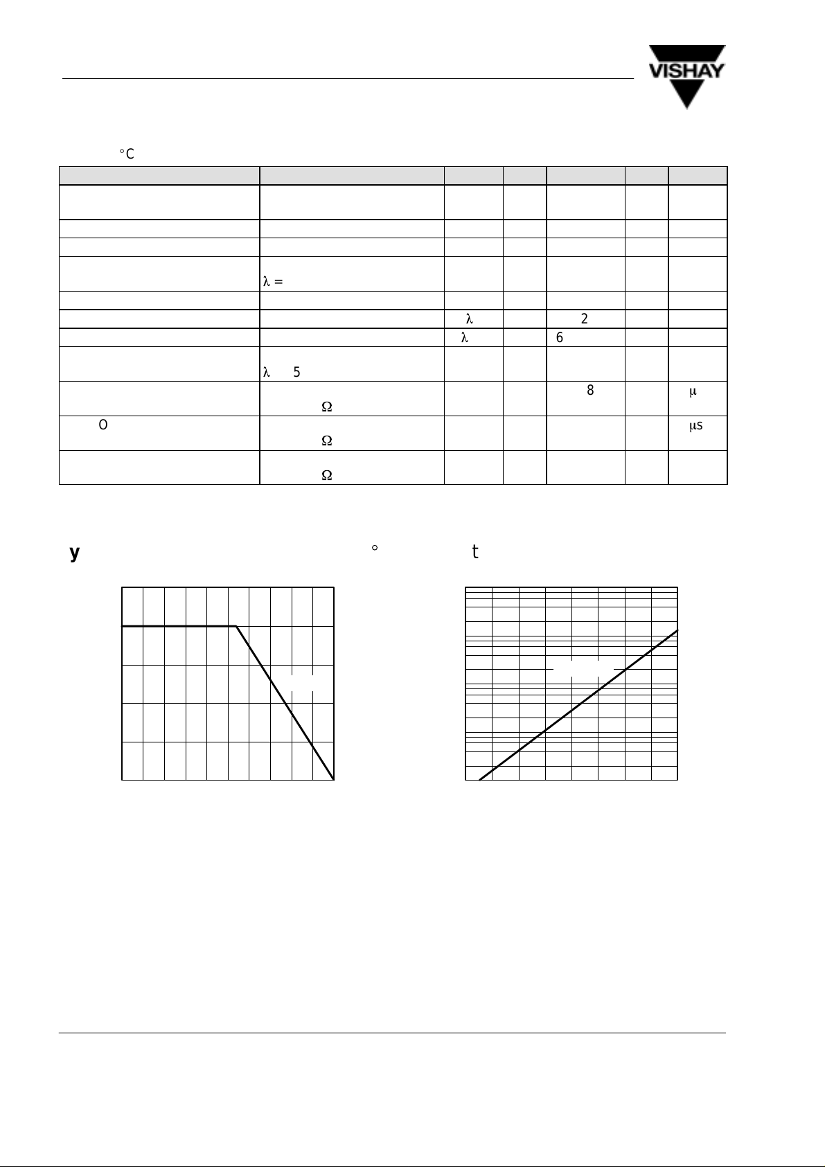
Figure 1. Total Power Dissipation vs.
– Ambient Temperature ( °C )
amb
Ambient Temperature
= 25_C unless otherwise specified)
amb
4
10
3
10
CEO
I – Collector Dark Current ( nA )
94 8235
2
10
1
10
0
10
20
40 60 80
T
– Ambient Temperature ( °C )
amb
R
thJA
100
Figure 2. Collector Dark Current vs. Ambient Temperature
VCE=20V
100
www.vishay.de • FaxBack +1-408-970-5600
2 (5) Rev. 2, 20-May-99
Document Number 81516
 Loading...