Surface Mount Schottky Barrier Diodes
Features
D
Low Turn–on Voltage
D
Fast Switching
D
PN Junction Guard Ring for Transient and ESD
Protection
Absolute Maximum Ratings
Tj = 25_C
Parameter Test Conditions Symbol Value Unit
Repetitive peak reverse voltage
=Working peak reverse voltage
=DC Blocking voltage
Peak forward surge current tp<1s , on fiberglass substrate I
Repetitive peak forward current on fiberglass substrate I
Average forward current I
Forward current on fiberglass substrate I
Power dissipation on fiberglass substrate P
Junction and storage
temperature range
V
=V
Tj=T
BAT54/A/C/S
Vishay Telefunken
94 8550
RRM
RWM
=V
FSM
FRM
FAV
R
F
d
stg
30 V
600 mA
300 mA
100 mA
200 mA
200 mW
–55...+125°C
Maximum Thermal Resistance
Tj = 25_C
Parameter Test Conditions Symbol Value Unit
Junction ambient R
Document Number 85508
Rev. 1, 01-Apr-99 1 (4)
thJA
www.vishay.de • FaxBack +1-408-970-5600
500 K/W

BAT54/A/C/S
g
Vishay Telefunken
Electrical Characteristics
Tj = 25_C
Parameter Test Conditions Symbol Min Typ Max Unit
Forward voltage IF=0.1mA, tp<300ms, duty cycle <2% V
IF=1mA, tp<300ms, duty cycle <2% V
IF=10mA, tp<300ms, duty cycle <2% V
IF=30mA, tp<300ms, duty cycle <2% V
IF=100mA, tp<300ms, duty cycle <2% V
Reverse current VR=25V, tp<300ms, duty cycle <2% I
Breakdown voltage IR=100mA V
Diode capacitance VR=1V, f=1MHz C
Reverse recovery time IF=10mA through IR=10mA to IR=1mA,
RL=100
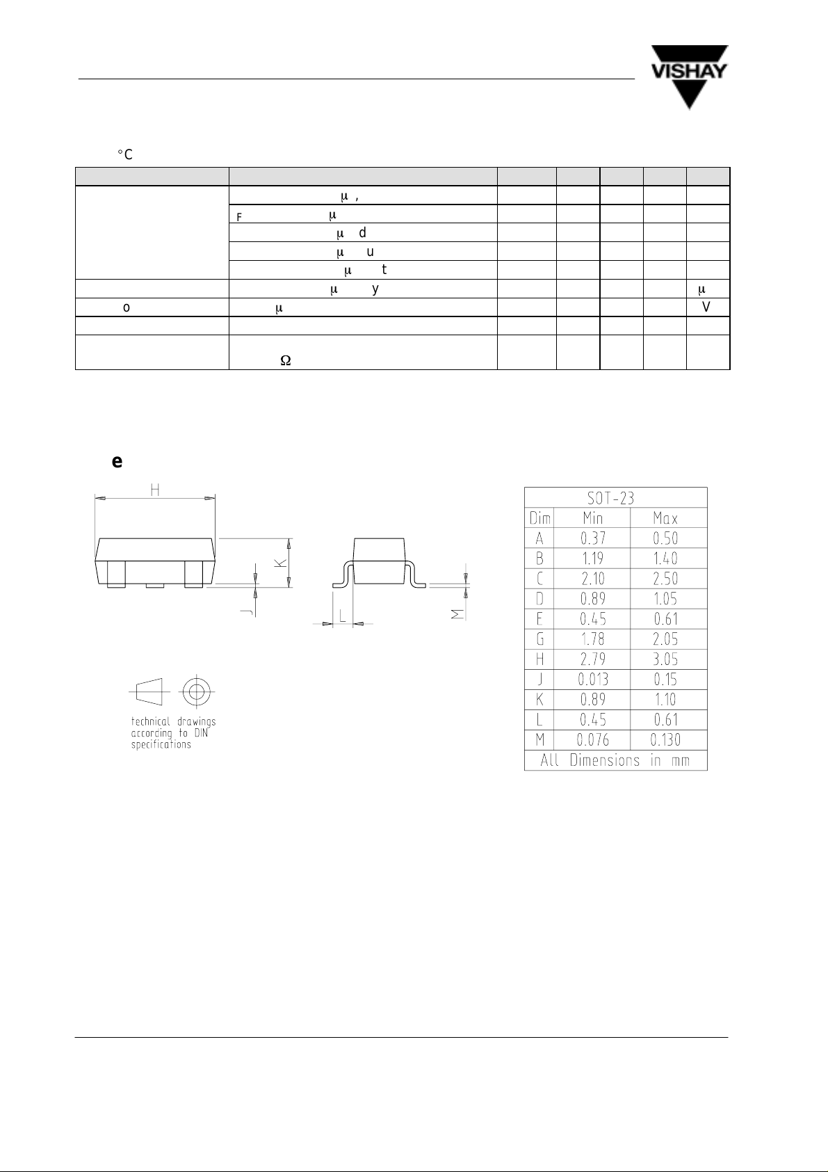
Dimensions in mm
W
F
F
F
F
F
R
(BR)
D
t
rr
240 mV
320 mV
400 mV
500 mV
1000 mV
2
m
30 V
10 pF
5 ns
A
14384
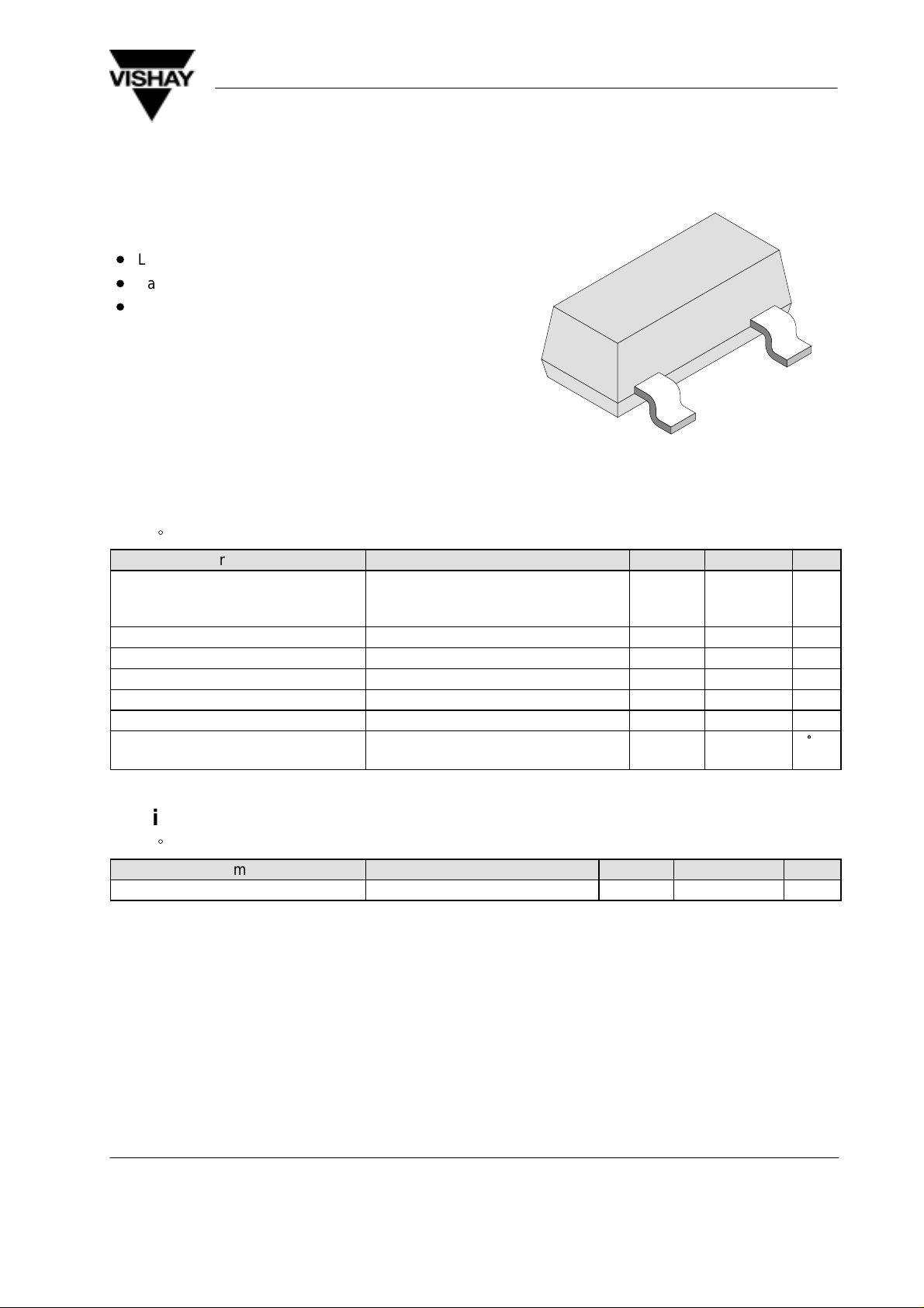
Case: SOT23, molded plastic
Terminals: Solderable per MIL–STD–202, Method 208
Polarity: see diagrams below
Mounting position: any
Approx. weight: 0.008 grams
www.vishay.de • FaxBack +1-408-970-5600 Document Number 85508
Rev. 1, 01-Apr-992 (4)
 Loading...