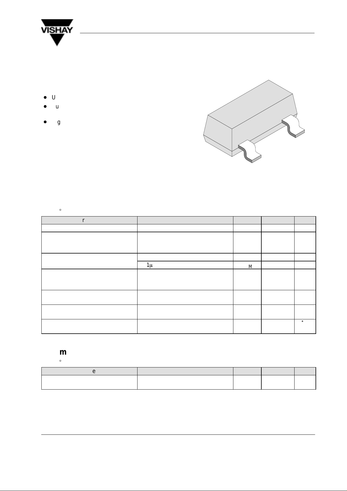
Silicon Epitaxial Planar Diode
g
Features
D
Ultra fast switching speed
D
Surface mount package ideally
suited for automatic insertion
D
High conductance
BAS16
Vishay Telefunken
94 8550
Absolute Maximum Ratings
Tj = 25_C
Parameter Test Conditions Symbol Value Unit
Non repetitive peak reverse voltage V
Repetitive peak reverse voltage
=Working peak reverse voltage
=DC Blocking voltage
Peak forward surge current tp=1s I
tp=1ms I
Average forward current half wave rectification with resistive
load and f ≥ 50 MHz, on ceramic
substrate 8mmx10mmx0.7mm
Forward current on ceramic substrate
8mmx10mmx0.7mm
Power dissipation on ceramic substrate
8mmx10mmx0.7mm
Junction and storage
temperature range
Maximum Thermal Resistance
Tj = 25_C
Parameter Test Conditions Symbol Value Unit
Junction ambient on ceramic substrate
8mmx10mmx0.7mm
V
=V
=V
FSM
FSM
I
FAV
P
Tj=T
R
RM
RRM
RWM
R
I
F
tot
stg
thJA
100 V
75 V
1 A
2 A
150 mA
300 mA
350 mW
–55...+150
357 K/W
°
C
Document Number 85539
Rev. 1, 01-Apr-99 1 (4)
www.vishay.de • FaxBack +1-408-970-5600

BAS16
g
Vishay Telefunken
Electrical Characteristics
Tj = 25_C
Parameter Test Conditions Symbol Min Typ Max Unit
Forward voltage IF=1mA V
IF=10mA V
IF=50mA V
IF=150mA V
Reverse current VR=75V I
VR=75V, Tj=150°C I
VR=25V, Tj=150°C I
Diode capacitance VR=0, f=1MHz C
Reverse recovery time IF=10mA to IR=1mA, VR=6V, RL=100
W
Characteristics (Tj = 25_C unless otherwise specified)
F
F
F
F
R
R
R
D
t
rr
715 mV
855 mV
1 V
1.25 V
1
m
50
30
m
m
4 pF
6 ns
A
A
A
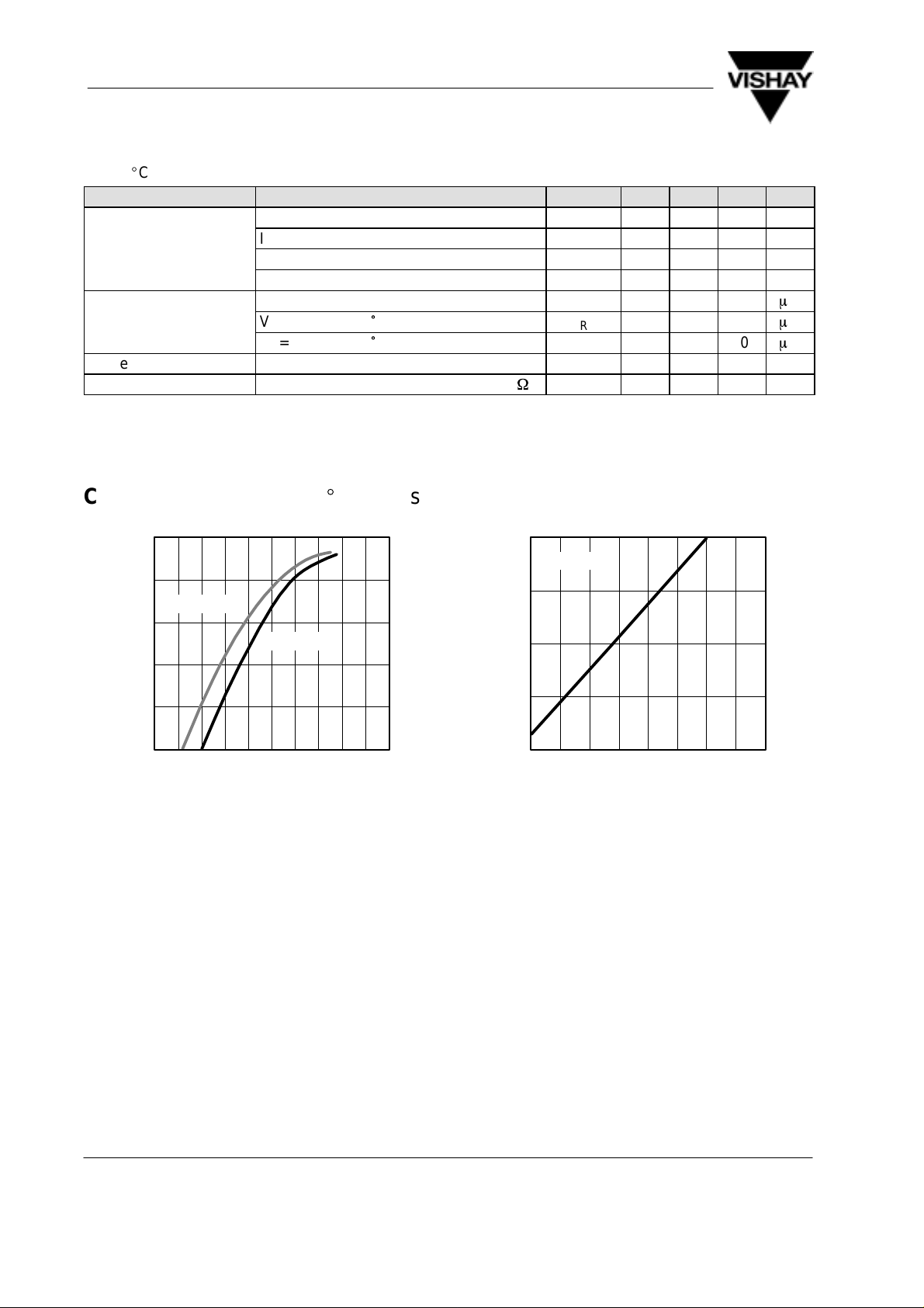
1000
100
Tj=100°C
10
Tj=25°C
1
0.1
F
I – Forward Current ( mA )
0.01
0 0.2 0.4 0.6 0.8 1.0 1.2 1.4 1.6 1.8 2.0
VF – Forward Voltage ( V )14356
Figure 1. Forward Current vs. Forward Voltage
10000
VR = 20 V
1000
100
10
R
I – Reverse Current ( nA )
1
0 25 50 75 100 125 150 175 200
Tj – Junction Temperature ( °C )14357
Figure 2. Reverse Current vs. Junction Temperature
www.vishay.de • FaxBack +1-408-970-5600 Document Number 85539
Rev. 1, 01-Apr-992 (4)
 Loading...