

Datasheet VS-VSK.166..PbF Series, VS-VSK.196..PbF Series, VS-VSK.236..PbF Series DataSheet (Vishay)
VS-VSK.166..PbF, VS-VSK.196..PbF, VS-VSK.236..PbF Series
INT-A-PAK
Standard Recovery Diodes, 165 A to 230 A
(INT-A-PAK Power Modules)
PRODUCT SUMMARY
I
F(AV)
Type Modules - Diode, High Voltage
Package INT-A-PAK
Circuit
Single diode, Two diodes common cathode,
Two diodes common cathode, Two diodes
165 A to 230 A
doubler circuit
Vishay Semiconductors
FEATURES
• High voltage
• Electrically isolated by DBC ceramic (AI
• 3500 V
isolating voltage
RMS
• Industrial standard package
• High surge capability
• Glass passivated chips
• Modules uses high voltage power diodes in four basic
configurations
• Simple mounting
• UL approved file E78996
• Designed and qualified for multiple level
• Material categorization: for definitions of compliance
please see www.vishay.com/doc?99912
APPLICATIONS
• DC motor control and drives
• Battery chargers
• Welders
• Power converters
2O3
)
MAJOR RATINGS AND CHARACTERISTICS
SYMBOL CHARACTERISTICS VSK.166.. VSK.196.. VSK.236.. UNITS
I
F(AV)
I
F(RMS)
I
FSM
2
I
t
2
I
t 798 1130 1516 kA2s
V
RRM
T
J
T
C
50 Hz 4000 4750 5500
60 Hz 4200 4980 5765
50 Hz 80 113 151
60 Hz 73 103 138
Range -40 to +150 °C
165 195 230 A
100 100 100 °C
260 305 360
400 to 1600 V
ELECTRICAL SPECIFICATIONS
VOLTAGE RATINGS
TYPE NUMBER
VS-VSK.166
VS-VSK.196
VS-VSK.236
, MAXIMUM REPETITIVE PEAK
V
VOLTAGE
CODE
04 400 500
08 800 900
12 1200 1300
14 1400 1500
16 1600 1700
RRM
REVERSE VOLTAGE
V
V
, MAXIMUM NON-REPETITIVE
RSM
PEAK REVERSE VOLTAGE
V
A
kA2s
I
RRM
AT 150 °C
mA
20
Revision: 02-Apr-15
1
Document Number: 94357
VS-VSK.166..PbF, VS-VSK.196..PbF, VS-VSK.236..PbF Series
Vishay Semiconductors
FORWARD CONDUCTION
PARAMETER SYMBOL TEST CONDITIONS VSK.166 VSK.196 VSK.236 UNITS
Maximum average on-state
current at case temperature
Maximum RMS on-state current I
Maximum peak, one-cycle
on-state, non-repetitive
surge current
Maximum I
Maximum I
2
t for fusing I2t
2
t for fusing I2t t = 0.1 ms to 10 ms, no voltage reapplied 798 1130 1516 kA2s
Low level value of threshold voltage V
High level value of threshold voltage V
Low level value on-state
slope resistance
High level value on-state
Maximum forward voltage drop V
I
F(AV)
F(RMS)
I
FSM
F(TO)1
F(TO)2
r
t1
r
t2
FM
180° conduction, half sine wave
t = 10 ms
t = 8.3 ms 4200 4980 5765
t = 10 ms
t = 8.3 ms 3500 4200 4850
t = 10 ms
t = 8.3 ms 73 103 138
t = 10 ms
t = 8.3 ms 52 73 98
(16.7 % x x I
(I > x I
(16.7 % x x I
(I > x I
IFM = x I
Average power = V
No voltage
reapplied
100 % V
reapplied
No voltage
reapplied
100 % V
RRM
RRM
Sine half wave,
initial T
=
J
T
maximum
J
reapplied
< I < x I
F(AV)
), TJ maximum 0.88 0.78 0.83
F(AV)
< I < x I
F(AV)
), TJ maximum 1.26 1.2 1.07
F(AV)
, TJ = 25 °C, 180° conduction
F(AV)
F(TO)
), TJ maximum 0.73 0.69 0.7
F(AV)
), TJ maximum 1.5 1.3 1.2
F(AV)
x I
+ rf x (I
F(AV)
F(RMS)
165 195 230 A
100 100 100 °C
260 305 360
4000 4750 5500
3350 4000 4630
80 113 151
56 80 107
1.43 1.38 1.46 V
2
)
A
kA2s
V
m
BLOCKING
PARAMETER SYMBOL TEST CONDITIONS VSK.166 VSK.196 VSK.236 UNITS
Maximum peak reverse and
off-state leakage current
RMS insulation voltage V
I
RRM
INS
TJ = 150 °C 20 mA
50 Hz, circuit to base, all terminals shorted,
t = 1 s
3500 V
THERMAL AND MECHANICAL SPECIFICATIONS
PARAMETER SYMBOL TEST CONDITIONS
Maximum junction operating and
storage temperature range
Maximum thermal resistance,
junction to case per junction
Maximum thermal resistance,
case to heatsink per module
Mounting
torque ± 10 %
IAP to heatsink
busbar to IAP
T
, T
J
Stg
R
thJC
R
thCS
DC operation 0.2 0.16 0.14
Mounting surface smooth, flat and greased 0.05
A mounting compound is recommended and
the torque should be rechecked after a period
VSK.166 VSK.196 VSK.236
of 3 hours to allow for the spread of
Approximate weight
the compound. Lubricated threads.
Case style INT-A-PAK
VALUES
UNITS
-40 to +150 °C
K/W
4 to 6 Nm
200 g
7.1 oz.
Revision: 02-Apr-15
2
Document Number: 94357
VS-VSK.166..PbF, VS-VSK.196..PbF, VS-VSK.236..PbF Series
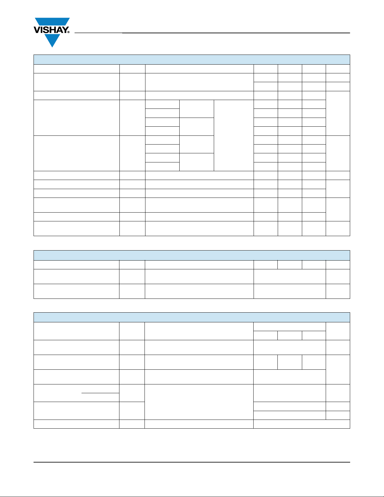
90
80
70
130
140
150
120
110
100
Maximum Allowable Case
Temperature (°C)
Average Forward Current (A)
50 100
150 200 250 300
0
DC
30°
60°
90°
120°
180°
VSK.166.. Series
R
thJC
(DC) = 0.20 K/W
Ø
Conduction period
0
50
200
150
100
Maximum Average Forward
Power Loss (W)
Average Forward Current (A)
10050 150 200
250 300
0
DC
180°
120°
90°
60°
30°
RMS limit
VSK.166.. Series
Per junction
T
J
= 150 °C
Ø
Conduction period
250
300
Vishay Semiconductors
R CONDUCTION PER JUNCTION
SINUSOIDAL CONDUCTION
MAXIMUM
AT T
DEVICES
J
180° 120° 90° 60° 30° 180° 120° 90° 60° 30°
VSK.166 0.025 0.03 0.038 0.055 0.089 0.018 0.031 0.041 0.057 0.089
VSK.236 0.009 0.010 0.014 0.018 0.025 0.008 0.012 0.015 0.019 0.025
Note
• Table shows the increment of thermal resistance R
when devices operate at different conduction angles than DC
thJC
RECTANGULAR CONDUCTION
AT TJ MAXIMUM
UNITS
K/WVSK.196 0.016 0.019 0.024 0.034 0.053 0.012 0.02 0.026 0.035 0.054
150
140
130
120
110
100
Temperature (°C)
90
Maximum Allowable Case
80
70
0
30°
40 80 120 160
Average Forward Current (A)
Fig. 1 - Current Ratings Characteristics
VSK.166.. Series
R
(DC) = 0.20 K/W
thJC
Conduction angle
60°
90°
120°
Ø
180°
200
250
200
150
100
180°
120°
90°
60°
30°
RMS limit
Power Loss (W)
50
Maximum Average Forward
0
0
Average Forward Current (A)
8040 120 160
Fig. 3 - On-State Power Loss Characteristics
Ø
Conduction angle
VSK.166.. Series
= 150 °C
T
J
200
Fig. 2 - Current Ratings Characteristics
Revision: 02-Apr-15
Fig. 4 - On-State Power Loss Characteristics
3
Document Number: 94357
VS-VSK.166..PbF, VS-VSK.196..PbF, VS-VSK.236..PbF Series
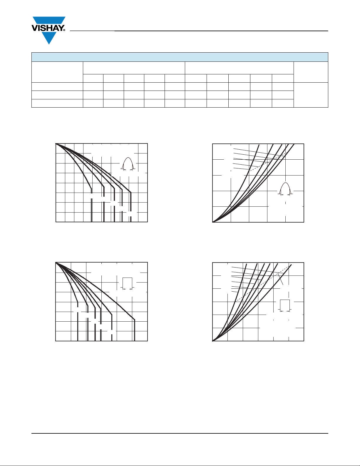
500
4000
3500
3000
2500
2000
1500
1000
Peak Half Sine Wave
Forward Current (A)
Pulse Train Duration (s)
0.1
1
0.01
Maximum non-repetitive surge current
Initial TJ = 150 °C
No voltage reapplied
Rated V
RRM
reapplied
versus pulse train duration.
VSK.166.. Series
0
100
150
200
250
300
50
Maximum Total Forward
Power Loss (W)
Total RMS Output Current (A)
50 100 150 200
250
0
DC
VSK.166.. Series
Per junction
T
J
= 150 °C
0
1200
1800
Maximum Total Power Loss (W)
Total Output Current (A)
0
180°
(Sine)
180°
(Rect)
2 x VSK.166.. Series
Single phase bridge
Connected
T
J
= 150 °C
+
-
~
1600
1400
1000
800
600
400
200
100
200
300
400
500
Vishay Semiconductors
4000
3500
3000
2500
2000
Forward Current (A)
Peak Half Sine Wave
1500
1000
At any rated load condition and with
rated V
VSK.166.. Series
Number of Equal Amplitude Half
applied following surge.
RRM
Initial TJ = 150 °C
at 60 Hz 0.0083 s
at 50 Hz 0.0100 s
10 1001
Cycle Current Pulses (N)
Fig. 5 - Maximum Non-Repetitive Surge Current Fig. 6 - Maximum Non-Repetitive Surge Current
300
250
200
150
0.4 K/W
0.5 K/W
0.7 K/W
0.3 K/W
0.2 K/W
R
thSA
= 0.12 K/W - ΔR
Revision: 02-Apr-15
100
Power Loss (W)
50
Maximum Total Forward
0
25 50 75 100 125
0
150
Maximum Allowable Ambient Temperature (°C)
Fig. 7 - On-State Power Loss Characteristics
1800
1600
1400
1200
1000
800
600
400
200
Maximum Total Power Loss (W)
0
R
thSA
= 0.12 K/W - ΔR
0.04 K/W
0.06 K/W
0.1 K/W
0.16 K/W
0.25 K/W
0.5 K/W
25 50 75 100 125
0
150
Maximum Allowable Ambient Temperature (°C)
Fig. 8 - On-State Power Loss Characteristics
4
Document Number: 94357

VS-VSK.166..PbF, VS-VSK.196..PbF, VS-VSK.236..PbF Series
0
800
600
400
200
1600
1400
1200
1000
Maximum Total Power Loss (W)
Total Output Current (A)
100 200 300 400
500
0
120°
(Rect)
3 x VSK.166.. Series
Three phase bridge
Connected
T
J
= 150 °C
-
~
70
100
110
120
130
140
150
90
80
Maximum Allowable Case
Temperature (°C)
Average Forward Current (A)
50 100 150 200 2500
30°
60°
90°
120°
180°
VSK.196.. Series
R
thJC
(DC) = 0.16 K/W
Ø
Conduction angle
70
100
110
120
130
140
150
90
80
Maximum Allowable Case
Temperature (°C)
Average Forward Current (A)
50 100 150 200 250
350300
0
DC
30°
60°
90°
120°
180°
VSK.196.. Series
R
thJC
(DC) = 0.16 K/W
Ø
Conduction period
0
200
250
300
150
100
50
Maximum Average Forward
Power Loss (W)
Average Forward Current (A)
40 80 120 160
200
0
RMS limit
180°
120°
90°
60°
30°
VSK.196.. Series
T
J
= 150 °C
Conduction angle
Ø
0
300
350
250
200
150
100
50
Maximum Average Forward
Power Loss (W)
Average Forward Current (A)
50 100 150 200 250 300
350
0
DC
180°
120°
90°
60°
30°
RMS limit
VSK.196.. Series
Per junction
T
J
= 150 °C
Ø
Conduction period
Vishay Semiconductors
1600
1400
1200
1000
Maximum Total Power Loss (W)
800
600
400
200
0.06 K/W
0.1 K/W
0.16 K/W
0.25 K/W
0.5 K/W
0
0
Maximum Allowable Ambient Temperature (°C)
Fig. 9 - On-State Power Loss Characteristics
0.04 K/W
25 50 75 100 125
R
thSA
= 0.02 K/W - ΔR
150
Fig. 10 - Current Ratings Characteristics
Revision: 02-Apr-15
Fig. 11 - Current Ratings Characteristics
Fig. 12 - On-State Power Loss Characteristics
Fig. 13 - On-State Power Loss Characteristics
5
Document Number: 94357

VS-VSK.166..PbF, VS-VSK.196..PbF, VS-VSK.236..PbF Series
4500
4000
3500
3000
2500
2000
1500
1000
Peal Half Sine Wave
Forward Current (A)
Number of Equal Amplitude Half
Cycle Current Pulses (N)
10
100
1
at 60 Hz 0.0083 s
at 50 Hz 0.0100 s
At any rated load condition and with
rated V
RRM
applied following surge.
VSK.196.. Series
Initial TJ = 150 °C
5000
4500
4000
3500
3000
2500
2000
1500
1000
Peak Half Sine Wave
Forward Current (A)
Pulse Train Duration (s)
0.1 1.00.01
Maximum non-repetitive surge current
Initial TJ = 150 °C
No voltage reapplied
Rated V
RRM
reapplied
versus pulse train duration.
VSK.196.. Series
0
200
250
300
350
150
100
50
Maximum Total Forward
Power Loss (W)
Total RMS Output Current (A)
50 100 150 200 250
300
0
DC
VSK.196.. Series
Per junction
T
J
= 150 °C
0
800
600
400
200
1200
1000
Maximum Total Power Loss (W)
Total Output Current (A)
100 200 300
400
0
180°
(Sine)
180°
(Rect)
2 x VSK.196.. Series
Single phase bridge
Connected
T
J
= 150 °C
+
-
~
Vishay Semiconductors
Fig. 14 - Maximum Non-Repetitive Surge Current Fig. 15 - Maximum Non-Repetitive Surge Current
Revision: 02-Apr-15
350
300
250
200
150
Power Loss (W)
100
Maximum Total Forward
0.4 K/W
0.5 K/W
0.7 K/W
50
0
0
Maximum Allowable Ambient Temperature (°C)
Fig. 16 - On-State Power Loss Characteristics
1200
800
600
400
200
0.08 K/W
0.12 K/W
0.16 K/W
0.25 K/W
0.4 K/W
0.7 K/W
1000
Maximum Total Power Loss (W)
0
0
Maximum Allowable Ambient Temperature (°C)
Fig. 17 - On-State Power Loss Characteristics
6
0.3 K/W
25 50 75 100 125
0.04 K/W
0.06 K/W
25
50 75 100
R
thSA
= 0.02 K/W - ΔR
= 0.12 K/W - ΔR
125
R
thSA
0.2 K/W
Document Number: 94357
150
150

VS-VSK.166..PbF, VS-VSK.196..PbF, VS-VSK.236..PbF Series
800
600
400
200
0
1800
1600
1400
1200
1000
Maximum Total Power Loss (W)
Total Output Current (A)
200100 300 400
500 600
0
120°
(Rect)
3 x VSK.196.. Series
Three phase bridge
Connected
T
J
= 150 °C
+
-
~
130
140
150
120
110
100
90
80
70
Maximum Allowable Case
Temperature (°C)
Average Forward Current (A)
50 100 150 200 300250 350
400
0
DC
VSK.236.. Series
R
thJC
(DC) = 0.14 K/W
Ø
Conduction period
120°
180°
90°
60°
30°
0
250
300
350
200
150
100
50
Maximum Average Forward
Power Loss (W)
Average Forward Current (A)
50 100 150 200
250
0
RMS limit
180°
120°
90°
60°
30°
VSK.236.. Series
T
J
= 150 °C
Conduction angle
Ø
0
350
400
450
300
250
200
150
100
50
Maximum Average Forward
Power Loss (W)
Average Forward Current (A)
50 100 150 200 300250 350
400
0
DC
180°
120°
90°
60°
30°
RMS limit
VSK.236.. Series
Per junction
T
J
= 150 °C
Ø
Conduction period
Vishay Semiconductors
1800
1600
0.06 K/W
1400
0.08 K/W
1200
1000
0.12 K/W
800
0.16 K/W
600
0.25 K/W
0.4 K/W
400
200
Maximum Total Power Loss (W)
0
0
Maximum Allowable Ambient Temperature (°C)
Fig. 18 - On-State Power Loss Characteristics
0.04 K/W
R
thSA
= 0.12 K/W - ΔR
5025 75 100
125
150
160
150
140
130
120
110
Temperature (°C)
100
Maximum Allowable Case
90
80
0
VSK.236.. Series
(DC) = 0.14 K/W
R
thJC
50
100 150 200
Average Forward Current (A)
Fig. 19 - Current Ratings Characteristics
30°
Ø
Conduction angle
60°
90°
120°
180°
250
Fig. 21 - On-State Power Loss Characteristics
Revision: 02-Apr-15
Fig. 20 - Current Ratings Characteristics
Fig. 22 - On-State Power Loss Characteristics
7
Document Number: 94357

VS-VSK.166..PbF, VS-VSK.196..PbF, VS-VSK.236..PbF Series
5000
3000
5500
4000
4500
3500
2500
2000
1500
1000
Peak Half Sine Wave
Forward Current (A)
Pulse Train Duration (s)
0.1 1.0
0.01
Maximum non-repetitive surge current
VSK.236.. Series
Initial TJ = 150 °C
No voltage reapplied
Rated V
RRM
reapplied
versus pulse train duration.
0
350
400
450
300
250
200
150
100
50
Maximum Total Forward
Power Loss (W)
Total RMS Output Current (A)
50 100 150 200 250 300
350
0
DC
VSK.236.. Series
Per junction
T
J
= 150 °C
0
350
400
450
300
250
200
150
100
50
Maximum Total Forward
Power Loss (W)
Maximum Allowable Ambient Temperature (°C)
25 50 75 100 125
150
0
0.16 K/W
0.25 K/W
0.35 K/W
0.5 K/W
0.7 K/W
R
thSA
= 0.1 K/W - ΔR
0
1000
1600
Maximum Total Power Loss (W)
Total Output Current (A)
100 200 300 400
500
0
180°
(Sine)
180°
(Rect)
2 x VSK.236.. Series
Single phase bridge
Connected
T
J
= 150 °C
+
-
~
1400
1200
800
600
400
200
0
800
600
400
200
1600
1400
1200
1000
Maximum Total Power Loss (W)
Maximum Allowable Ambient Temperature (°C)
5025 75 100
125 150
0
0.04 K/W
0.06 K/W
0.08 K/W
0.12 K/W
0.16 K/W
0.25 K/W
0.4 K/W
R
thSA
= 0.02 K/W - ΔR
Vishay Semiconductors
5000
4500
4000
3500
3000
2500
Forward Curren (A)
Peak Half Sine Wave
2000
1500
1
At any rated load condition and with
rated V
VSK.236.. Series
applied following surge.
RRM
10
Initial TJ = 150 °C
at 60 Hz 0.0083 s
at 50 Hz 0.0100 s
100
Number of Equal Amplitude Half
Cycle Current Pulse (A)
Fig. 23 - Maximum Non-Repetitive Surge Current Fig. 24 - Maximum Non-Repetitive Surge Current
Revision: 02-Apr-15
Fig. 25 - On-State Power Loss Characteristics
Fig. 26 - On-State Power Loss Characteristics
8
Document Number: 94357

VS-VSK.166..PbF, VS-VSK.196..PbF, VS-VSK.236..PbF Series
0
500
2500
2000
1500
1000
Maximum Total Power Loss (W)
Total Output Current (A)
200100 300 400
700
500 600
0
120°
(Rect)
3 x VSK.236.. Series
Three phase bridge
Connected
T
J
= 150 °C
+
-
~
1
100
10
10 000
1000
Instantaneous On-State Current (A)
Instantaneous On-State Voltage (V)
0.5 1.0 1.5 2.0 3.02.5 3.5
4.0
0
TJ = 25 °C
VSK.166.. Series
Per junction
TJ = 150 °C
1
100
10
10 000
1000
Instantaneous On-State Current (A)
Instantaneous On-State Voltage (V)
1.0 2.0 3.0 4.0
5.0
0
TJ = 25 °C
TJ = 150 °C
VSK.196.. Series
Per junction
1
100
10
10 000
1000
Instantaneous On-State Current (A)
Instantaneous On-State Voltage (V)
1.0 2.0 3.0 4.0 5.00
TJ = 25 °C
TJ = 150 °C
VSK.236.. Series
Per junction
0.01
0.1
1
Z
thJC
- Transient Thermal Impedance
Square Wave Pulse Duration (s)
10.1
10
0.01
VSK.166.. Series
Steady state value
(DC operation)
Vishay Semiconductors
2500
R
0.04 K/W
thSA
= 0.02 K/W - ΔR
5025 75 100
125
150
2000
0.06 K/W
1500
0.1 K/W
1000
0.16 K/W
0.3 K/W
500
Maximum Total Power Loss (W)
0.7 K/W
0
0
Maximum Allowable Ambient Temperature (°C)
Fig. 27 - On-State Power Loss Characteristics
Fig. 28 - On-State Voltage Drop Characteristics
Revision: 02-Apr-15
Fig. 29 - On-State Voltage Drop Characteristics
Fig. 30 - On-State Voltage Drop Characteristics
Fig. 31 - Thermal Impedance Z
9
Characteristics
thJC
Document Number: 94357

VS-VSK.166..PbF, VS-VSK.196..PbF, VS-VSK.236..PbF Series
Vishay Semiconductors
1
Steady state value
(DC operation)
0.1
- Transient Thermal Impedance
thJC
0.01
Z
0.01
VSK.196.. Series
0.1 1.0
Square Wave Pulse Duration (s)
Fig. 32 - Thermal Impedance Z
Characteristics Fig. 33 - Thermal Impedance Z
thJC
ORDERING INFORMATION TABLE
Device code
10
VS-VS 236 16 PbFKD
1 3
1
Steady state value
(DC operation)
0.1
- Transient Thermal Impedance
thJC
0.01
Z
0.01
VSK.236.. Series
0.1 1.0
Square Wave Pulse Duration (s)
52 4
Characteristics
thJC
10
- Vishay Semiconductors product
1
2 - Circuit configuration
3
- Current rating: I
F(AV)
4 - Voltage code x 100 = V
5
- PbF = Lead (Pb)-free
RRM
Revision: 02-Apr-15
10
Document Number: 94357

VS-VSK.166..PbF, VS-VSK.196..PbF, VS-VSK.236..PbF Series
VSKE...
-+
+
-
CIRCUIT CONFIGURATION
CIRCUIT DESCRIPTION
CIRCUIT
CONFIGURATION CODE
Vishay Semiconductors
CIRCUIT DRAWING
VSKD...
~-+
Two diodes doubler circuit D
Two diodes common cathodes C
Two diodes common anodes J
Single diode E
~
VSKC...
+
VSKJ...
- ++
-
+
-
-
-
+
-
-+
+
Dimensions www.vishay.com/doc?95254
Revision: 02-Apr-15
LINKS TO RELATED DOCUMENTS
11
Document Number: 94357

DIMENSIONS in millimeters (inches)
17 (0.67)
23 (0.91)
23 (0.91)
3 screws M6 x 10
66 (2.60)
94 (3.70)
35 (1.38)
14.5
(0.57)
1
2
3
5
4
37 (1.44)
80 (3.15)
Ø 6.5 (Ø 0.25)
30 (1.18)
9 (0.33)
28 (1.10)
7
6
Outline Dimensions
Vishay Semiconductors
INT-A-PAK DBC
Document Number: 95254
Revision: 11-Dec-07 1

Legal Disclaimer Notice
Vishay
Disclaimer
ALL PRODUCT, PRODUCT SPECIFICATIONS AND DATA ARE SUBJECT TO CHANGE WITHOUT NOTICE TO IMPROVE
RELIABILITY, FUNCTION OR DESIGN OR OTHERWISE.
Vishay Intertechnology, Inc., its affiliates, agents, and employees, and all persons acting on its or their behalf (collectively,
“Vishay”), disclaim any and all liability for any errors, inaccuracies or incompleteness contained in any datasheet or in any other
disclosure relating to any product.
Vishay makes no warranty, representation or guarantee regarding the suitability of the products for any particular purpose or
the continuing production of any product. To the maximum extent permitted by applicable law, Vishay disclaims (i) any and all
liability arising out of the application or use of any product, (ii) any and all liability, including without limitation special,
consequential or incidental damages, and (iii) any and all implied warranties, including warranties of fitness for particular
purpose, non-infringement and merchantability.
Statements regarding the suitability of products for certain types of applications are based on Vishay’s knowledge of typical
requirements that are often placed on Vishay products in generic applications. Such statements are not binding statements
about the suitability of products for a particular application. It is the customer’s responsibility to validate that a particular
product with the properties described in the product specification is suitable for use in a particular application. Parameters
provided in datasheets and/or specifications may vary in different applications and performance may vary over time. All
operating parameters, including typical parameters, must be validated for each customer application by the customer’s
technical experts. Product specifications do not expand or otherwise modify Vishay’s terms and conditions of purchase,
including but not limited to the warranty expressed therein.
Except as expressly indicated in writing, Vishay products are not designed for use in medical, life-saving, or life-sustaining
applications or for any other application in which the failure of the Vishay product could result in personal injury or death.
Customers using or selling Vishay products not expressly indicated for use in such applications do so at their own risk. Please
contact authorized Vishay personnel to obtain written terms and conditions regarding products designed for such applications.
No license, express or implied, by estoppel or otherwise, to any intellectual property rights is granted by this document or by
any conduct of Vishay. Product names and markings noted herein may be trademarks of their respective owners.
Material Category Policy
Vishay Intertechnology, Inc. hereby certifies that all its products that are identified as RoHS-Compliant fulfill the
definitions and restrictions defined under Directive 2011/65/EU of The European Parliament and of the Council
of June 8, 2011 on the restriction of the use of certain hazardous substances in electrical and electronic equipment
(EEE) - recast, unless otherwise specified as non-compliant.
Please note that some Vishay documentation may still make reference to RoHS Directive 2002/95/EC. We confirm that
all the products identified as being compliant to Directive 2002/95/EC conform to Directive 2011/65/EU.
Vishay Intertechnology, Inc. hereby certifies that all its products that are identified as Halogen-Free follow Halogen-Free
requirements as per JEDEC JS709A standards. Please note that some Vishay documentation may still make reference
to the IEC 61249-2-21 definition. We confirm that all the products identified as being compliant to IEC 61249-2-21
conform to JEDEC JS709A standards.
Revision: 02-Oct-12
1
Document Number: 91000
 Loading...