

Page 1
www.vishay.com
B-8
(Stud Version), 400 A, 450 A
PRODUCT SUMMARY
I
F(AV)
Package B-8
Circuit configuration Single diode
400 A, 450 A
Fast Recovery Diodes
FEATURES
• High power fast recovery diode series
• 2.0 μs to 3.0 μs recovery time
• High voltage ratings up to 2500 V
• High current capability
• Optimized turn-on and turn-off characteristics
• Low forward recovery
• Fast and soft reverse recovery
• Compression bonded encapsulation
• Stud version case style B-8
• Maximum junction temperature 150 °C
• Designed and qualified for industrial level
• Material categorization: For definitions of compliance
please see www.vishay.com/doc?99912
TYPICAL APPLICATIONS
• Snubber diode for GTO
• High voltage freewheeling diode
• Fast recovery rectifier applications
VS-SD453N/R Series
Vishay Semiconductors
MAJOR RATINGS AND CHARACTERISTICS
PARAMETER TEST CONDITIONS
I
F(AV)
I
F(RMS)
I
FSM
V
RRM
t
rr
T
J
T
C
50 Hz 9300 9600
60 Hz 9730 10 050
Range 1200 to 2500 1200 to 2500 V
T
J
ELECTRICAL SPECIFICATIONS
VOLTAGE RATINGS
, MAXIMUM REPETITIVE
V
TYPE NUMBER
VS-SD453N/R
VOLTAGE
CODE
12 1200 1300
16 1600 1700
20 2000 2100
25 2500 2600
RRM
PEAK REVERSE VOLTAGE
V
SD453N/R
S20 S30
400 450 A
70 70 °C
630 710
2.0 3.0 μs
25 25
- 40 to 150 - 40 to 150
V
, MAXIMUM NON-REPETITIVE
RSM
PEAK REVERSE VOLTAGE
V
UNITS
I
MAXIMUM
RRM
AT T
= TJ MAXIMUM
J
A
°C
mA
50
Revision: 21-Jan-14
For technical questions within your region: DiodesAmericas@vishay.com
THIS DOCUMENT IS SUBJECT TO CHANGE WITHOUT NOTICE. THE PRODUCTS DESCRIBED HEREIN AND THIS DOCUMENT
ARE SUBJECT TO SPECIFIC DISCLAIMERS, SET FORTH AT www.vishay.com/doc?91000
1
, DiodesAsia@vishay.com, DiodesEurope@vishay.com
Document Number: 93176
Page 2
www.vishay.com
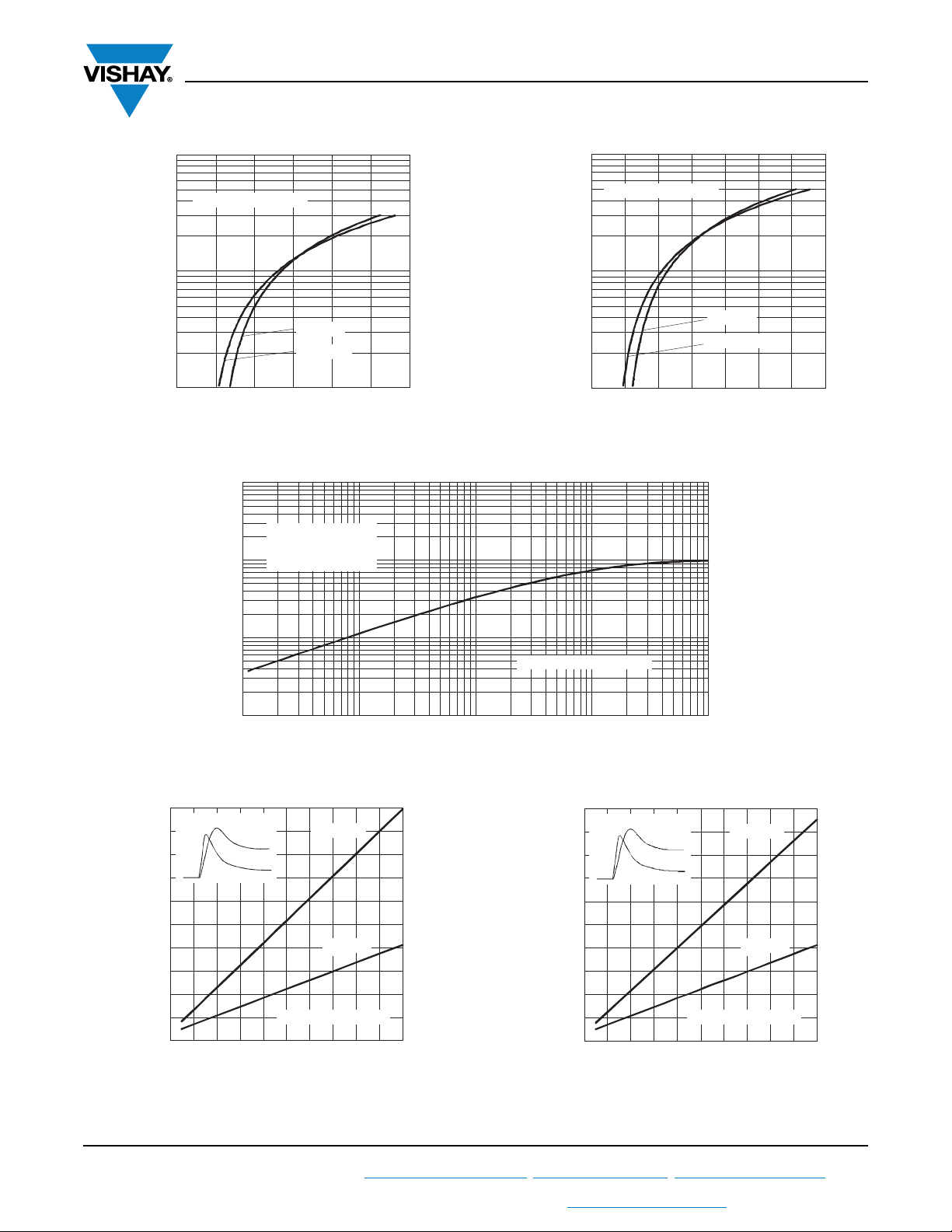
FORWARD CONDUCTION
PARAMETER SYMBOL TEST CONDITIONS
Maximum average forward current
at case temperature
Maximum RMS forward current at
case temperature
I
Maximum peak, one-cycle forward,
non-repetitive surge current
Maximum I
Maximum I
2
t for fusing I2t
2
t for fusing I2t t = 0.1 to 10 ms, no voltage reapplied 4320 4600 kA2s
Low level value of threshold voltage V
High level value of threshold voltage V
Low level value of forward
slope resistance
High level value of forward
slope resistance
Maximum forward voltage drop V
I
F(AV)
F(RMS)
I
FSM
F(TO)1
F(TO)2
r
r
180° conduction, half sine wave
t = 10 ms
t = 8.3 ms 9730 10 050
t = 10 ms
t = 8.3 ms 8190 8450
t = 10 ms
t = 8.3 ms 395 420
t = 10 ms
t = 8.3 ms 279 297
(16.7 % x x I
T
= TJ maximum
J
(I > x I
(16.7 % x x I
f1
T
= TJ maximum
J
(I > x I
f2
Ipk = 1500 A, TJ = TJ maximum,
FM
t
= 10 ms sinusoidal wave
p
No voltage
reapplied
100 % V
reapplied
No voltage
reapplied
100 % V
reapplied
F(AV)
), TJ = TJ maximum 1.09 1.04
F(AV)
F(AV)
), TJ = TJ maximum 0.74 0.54
F(AV)
RRM
RRM
< I < x I
< I < x I
Sinusoidal half wave,
initial T
maximum
),
F(AV)
),
F(AV)
= TJ
J
VS-SD453N/R Series
Vishay Semiconductors
SD453N/R
S20 S30
400 450 A
70 70 °C
630 710 A
55 52 °C
9300 9600
7820 8070
432 460
306 326
1.00 0.95
0.80 0.60
2.20 1.85 V
UNITS
A
kA2s
V
mW
RECOVERY CHARACTERISTICS
TYPICAL VALUES
AT TJ = 150 °C
AT 25 % I
(μs)
RRM
Q
(μC)
rr
3.5 250 120
I
(A)
I
FM
rr
t
rr
dir
dt
CODE
MAXIMUM VALUE
= 25 °C
AT T
J
AT 25 % I
t
rr
RRM
(μs)
TEST CONDITIONS
I
pk
SQUARE
PULSE
dI/dt
(A/μs)
V
(V)
t
r
rr
(A)
S20 2.0
S30 3.0 5.0 380 150
1000 50 - 50
THERMAL AND MECHANICAL SPECIFICATIONS
PARAMETER SYMBOL TEST CONDITIONS VALUES UNITS
Maximum junction operating and storage
temperature range
Maximum thermal resistance, junction to case R
Maximum thermal resistance, case to heatsink R
Mounting torque ± 10 % Not-lubricated threads 50 Nm
Approximate weight 454 g
Case style See dimensions (link at the end of datasheet) B-8
R
CONDUCTION
thJC
CONDUCTION ANGLE SINUSOIDAL CONDUCTION RECTANGULAR CONDUCTION TEST CONDITIONS UNITS
180° 0.010 0.008
120° 0.014 0.014
90° 0.017 0.019
60° 0.025 0.026
30° 0.042 0.042
Note
• The table above shows the increment of thermal resistance R
Revision: 21-Jan-14
For technical questions within your region: DiodesAmericas@vishay.com
THIS DOCUMENT IS SUBJECT TO CHANGE WITHOUT NOTICE. THE PRODUCTS DESCRIBED HEREIN AND THIS DOCUMENT
ARE SUBJECT TO SPECIFIC DISCLAIMERS, SET FORTH AT www.vishay.com/doc?91000
TJ, T
thJC
thCS
Stg
DC operation 0.1
Mounting surface, smooth, flat and greased 0.04
when devices operate at different conduction angles than DC
thJC
2
, DiodesAsia@vishay.com, DiodesEurope@vishay.com
- 40 to 150 °C
T
= TJ maximum K/W
J
Document Number: 93176
I
RM(REC)
K/W
t
Q
rr
Page 3
www.vishay.com
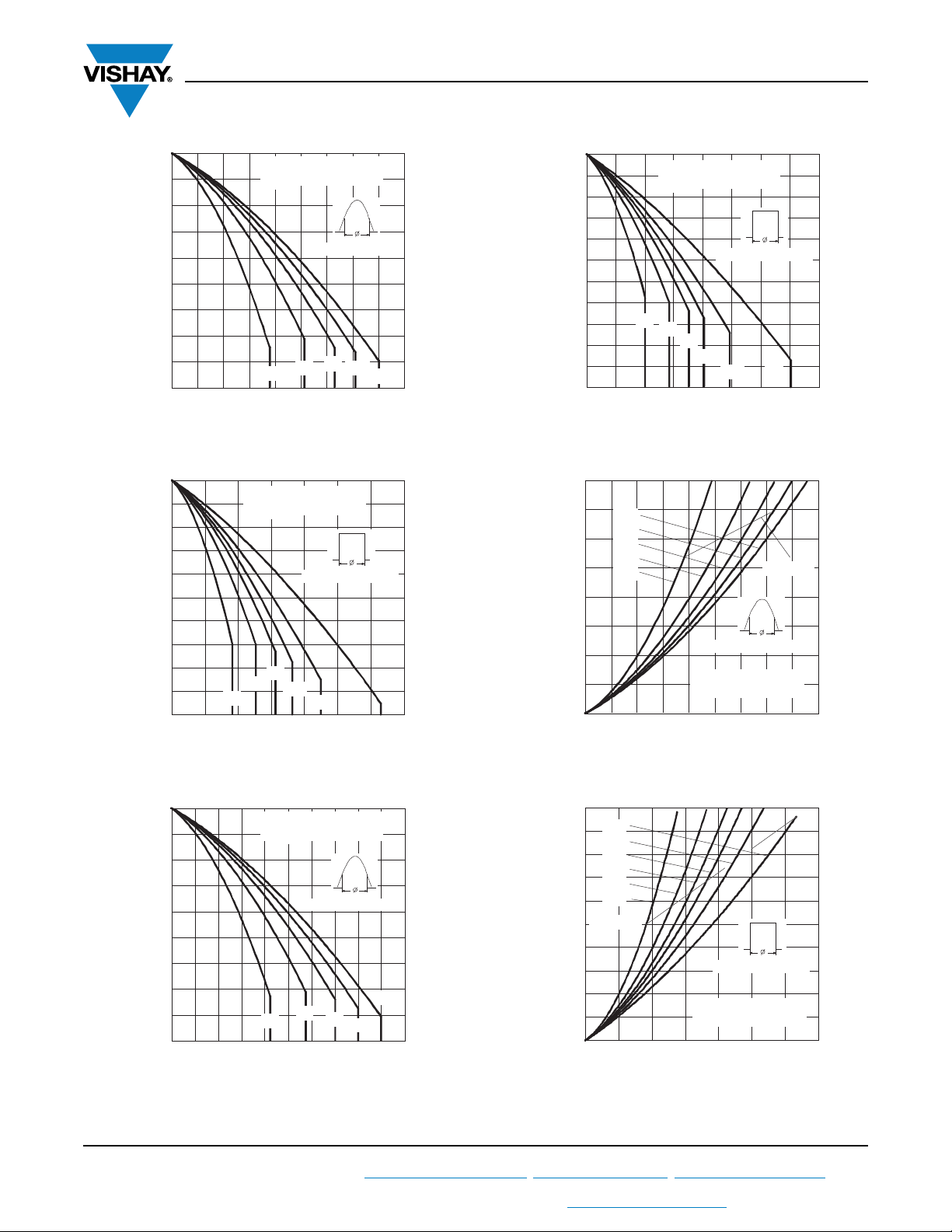
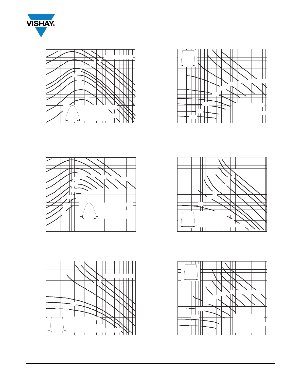
60
70
80
90
100
110
120
130
140
150
0100200300400500
30°
60°
90°
120°
180°
Average Forward Current (A)
Cond uc tion Ang le
Maximum Allo wab le Case Te mperature (°C)
SD 4 5 3 N/ R. . S3 0 Se r i e s
R (DC ) = 0.1 K/W
thJC
40
50
60
70
80
90
100
110
120
130
140
150
0 200 400 600 800
30°
60°
90°
180°
DC
120°
Average Forward Current (A)
Conduction Period
Maximum Allowable Case Temperature (°C)
SD 45 3 N/ R. . S3 0 Se r i e s
R ( DC) = 0.1 K/ W
thJC
VS-SD453N/R Series
Vishay Semiconductors
150
140
SD 45 3N / R. . S2 0 Se r i e s
R (DC ) = 0.1 K/ W
thJC
130
120
110
Cond uctio n Angle
100
90
80
70
60
Maximum Allowable Case Temperature (°C)
0 50 100 150 200 250 300 350 400 450
30°
60°
90°
Average Forward Current (A)
Fig. 1 - Current Ratings Characteristics
150
140
SD 45 3 N / R. . S2 0 Se r i e s
R ( DC) = 0.1 K/ W
thJC
130
120
110
Cond uc tion Period
100
90
80
70
60
50
Maximum Allowable Case Temp erature (°C)
0 100 200 300 400 500 600 700
30°
60°
90°
120°
180°
Average Forward Current (A)
Fig. 2 - Current Ratings Characteristics
120°
DC
180°
Fig. 4 - Current Ratings Characteristics
800
700
600
500
400
300
200
100
Maximum Average Forward Power Loss (W)
180°
120°
90°
60°
30°
Cond uc tion Ang le
SD 45 3 N / R . . S2 0 Se r i e s
T = 150°C
J
0
0 50 100 150 200 250 300 350 400 450
Average Forward Current (A)
RM S Li m it
Fig. 5 - Forward Power Loss Characteristics
Revision: 21-Jan-14
Fig. 3 - Current Ratings Characteristics
For technical questions within your region: DiodesAmericas@vishay.com
THIS DOCUMENT IS SUBJECT TO CHANGE WITHOUT NOTICE. THE PRODUCTS DESCRIBED HEREIN AND THIS DOCUMENT
ARE SUBJECT TO SPECIFIC DISCLAIMERS, SET FORTH AT www.vishay.com/doc?91000
1000
900
800
700
600
500
400
300
200
100
Maximum Average Forward Power Loss (W)
DC
180°
120°
90°
60°
30°
RM S Lim i t
Conduction Period
SD 45 3N / R . . S20 Se r i e s
T = 150°C
J
0
0 100 200 300 400 500 600 700
Average Forward Current (A)
Fig. 6 - Forward Power Loss Characteristics
3
Document Number: 93176
, DiodesAsia@vishay.com, DiodesEurope@vishay.com
Page 4
www.vishay.com
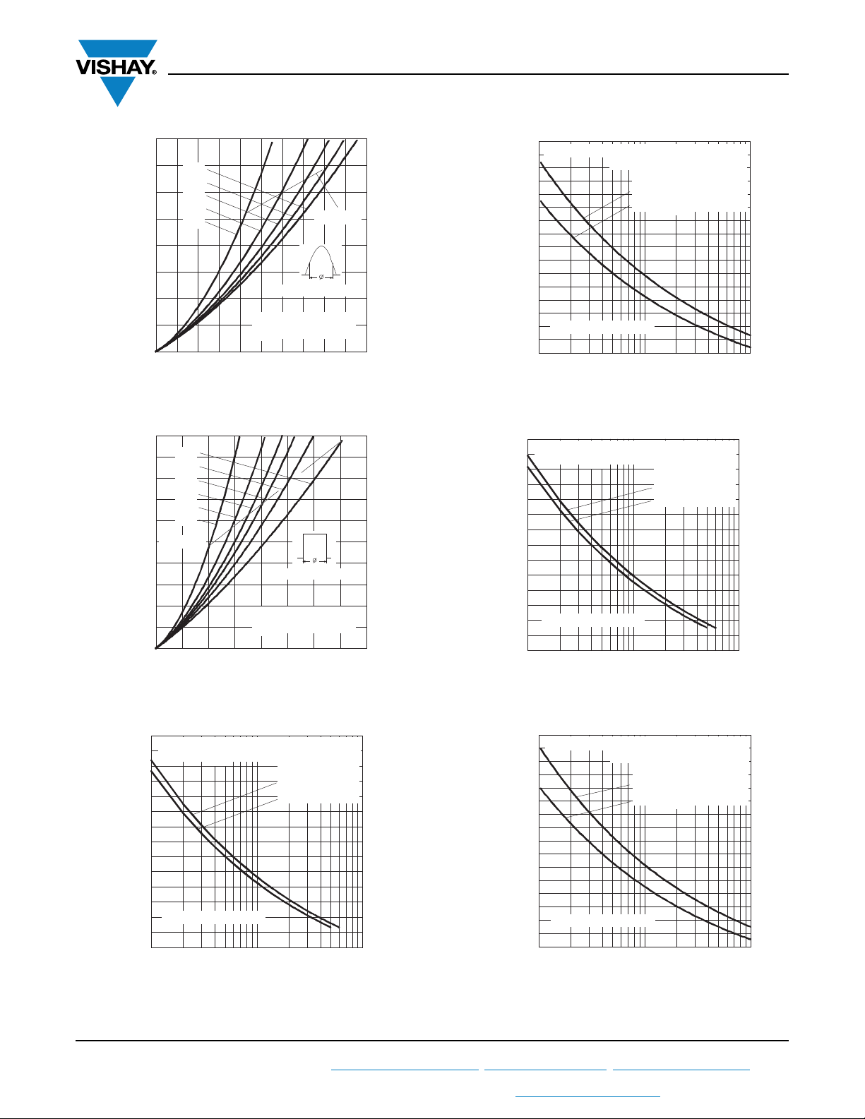
0
100
200
300
400
500
600
700
800
0 100 200 300 400 500
180°
120°
90°
60°
30°
Avera ge Forward Curre nt (A)
Maximum Average Forw ard Power Loss (W)
RM S Li m i t
Conduction Angle
SD 4 5 3 N / R. . S3 0 Se r i e s
T = 1 5 0 ° C
J
0
100
200
300
400
500
600
700
800
900
1000
0 100 200 300 400 500 600 700 800
DC
180°
120°
90°
60°
30°
Average Forward Current (A)
RM S Li m i t
Maximum Avera ge Forward Power Loss (W)
Cond uction Period
SD 45 3 N / R. . S30 Se r i e s
T = 1 50 ° C
J
2000
3000
4000
5000
6000
7000
8000
9000
10000
0.01 0.1 1
Pulse Tra in D u r a t io n (s)
Peak Half Sine Wave Forward Current (A)
Maximum Non Repetitive Surge Current
SD453N/ R..S20 Se ries
Versus Pulse Train Duration.
Initial T = 150 °C
No Voltage Reapplied
Rated V Reapplied
RRM
J
2000
3000
4000
5000
6000
7000
8000
9000
10000
0.01 0.1 1
Pulse Train Duration (s)
Pea k Ha lf Sine Wave Forward Current (A)
Maximum Non Repetitive Surge Current
SD453N/ R..S30 Serie s
Versus Pulse Train Duration.
Init ia l T = 150 °C
No Volta g e Re ap p lied
Rated V Reapplied
RRM
J
VS-SD453N/R Series
Vishay Semiconductors
Fig. 7 - Forward Power Loss Characteristics
Fig. 8 - Forward Power Loss Characteristics
9000
At Any Rated Load Condition And With
Rated V Applied Following Surge.
8000
7000
RRM
Initia l T = 150 °C
J
@ 60 Hz 0.0083 s
@ 50 Hz 0.0100 s
Fig. 10 - Maximum Non-Repetitive Surge Current
9000
At An y Rat ed Loa d Condition An d With
Rated V Applied Following Surge.
8000
7000
6000
5000
4000
3000
Pea k Ha lf Sine Wave Forward Current (A)
2000
Number Of Eq ual Amplitud e Half Cyc le Current Pulses (N)
SD 45 3 N/ R . . S3 0 Se r i e s
110100
RRM
Init ial T = 150 °C
J
@ 60 Hz 0.0083 s
@ 50 Hz 0.0100 s
Fig. 11 - Maximum Non-Repetitive Surge Current
6000
Revision: 21-Jan-14
5000
4000
3000
Peak Half Sine Wa ve Forwa rd Current (A)
2000
Number Of Eq ual Amplitude Half Cycle Current Pulses (N)
Fig. 9 - Maximum Non-Repetitive Surge Current
For technical questions within your region: DiodesAmericas@vishay.com
SD453N/ R..S20 Se ries
110100
THIS DOCUMENT IS SUBJECT TO CHANGE WITHOUT NOTICE. THE PRODUCTS DESCRIBED HEREIN AND THIS DOCUMENT
Fig. 12 - Maximum Non-Repetitive Surge Current
4
, DiodesAsia@vishay.com, DiodesEurope@vishay.com
ARE SUBJECT TO SPECIFIC DISCLAIMERS, SET FORTH AT www.vishay.com/doc?91000
Document Number: 93176
Page 5
VS-SD453N/R Series
100
1000
10000
0.5 1 1.5 2 2. 5 3 3.5 4
T = 2 5° C
J
Instantaneous Forward Voltage (V)
Instantaneous Forward Current (A)
T = 150°C
J
SD453N/ R. .S30 Se ries
0
20
40
60
80
100
0 400 800 120016002000
T = 2 5 ° C
J
Forwa rd Rec overy (V)
T = 1 5 0 °C
J
SD 45 3 N/ R . . S3 0 Se r i e s
Rate Of Rise Of Forward Current - di/dt (A/us)
I
V
FP
www.vishay.com
10000
SD453N/ R..S20 Serie s
1000
T = 2 5 ° C
J
T = 150°C
Instantaneous Forwa rd Current (A)
100
0.5 1 1.5 2 2.5 3 3.5
Instantaneous Forward Voltage (V)
Fig. 13 - Forward Voltage Drop Characteristics Fig. 14 - Forward Voltage Drop Characteristics
1
J
Vishay Semiconductors
thJC
0.1
0.01
Transient Thermal Impedance Z (K/W)
0.001
0.001 0.01 0.1 1 10
100
V
FP
80
60
Revision: 21-Jan-14
40
Fo rw a rd Rec ove ry (V)
20
0
0 400 800 1200 1600 2000
Rate Of Rise Of Forw ard Current - di/dt (A/us)
Fig. 16 - Typical Forward Recovery Characteristics Fig. 17 - Typical Forward Recovery Characteristics
For technical questions within your region: DiodesAmericas@vishay.com
THIS DOCUMENT IS SUBJECT TO CHANGE WITHOUT NOTICE. THE PRODUCTS DESCRIBED HEREIN AND THIS DOCUMENT
ARE SUBJECT TO SPECIFIC DISCLAIMERS, SET FORTH AT www.vishay.com/doc?91000
Steady Sta te Value:
R = 0.1 K/W
thJC
(DC Operation)
T = 150°C
I
J
T = 2 5 ° C
J
SD 45 3 N / R . . S20 Se r i e s
Sq u a r e W a v e P u l se D u ra t i o n ( s)
Fig. 15 - Thermal Impedance Z
5
SD453N/ R..S20/ S30 Se rie s
Characteristic
thJC
Document Number: 93176
, DiodesAsia@vishay.com, DiodesEurope@vishay.com
Page 6

www.vishay.com
0
100
200
300
400
500
600
700
800
0 50 100 150 200 250 300
Maximum Reverse Rec overy Charge - Qrr (µC)
Rate Of Fall Of Forward Current - di/dt (A/µs)
500 A
150 A
I = 1000 A
Si n e Pu l s e
FM
SD 45 3N / R. . S2 0 Se r ie s
T = 150 °C; V > 100V
J
r
VS-SD453N/R Series
Vishay Semiconductors
6
SD 45 3 N / R. . S2 0 Se r i e s
5.5
T = 150 °C; V > 100V
J
r
5
4.5
4
3.5
I = 1000 A
FM
Si n e Pu l se
500 A
150 A
3
2.5
Maximum Reverse Rec overy Time - Trr (µs)
2
10 100 1000
Rate Of Fall Of Forward Current - di/dt (A/µs)
Fig. 18 - Recovery Time Characteristics
7
6.5
SD453N/ R..S30 Se rie s
T = 150 °C, V > 100V
J
r
6
5.5
I = 1000 A
5
4.5
4
FM
Si n e Pu l se
500 A
150 A
3.5
3
2.5
Maximum Reverse Recovery Time - Trr (µs)
2
10 100 1000
Rate Of Fall Of Forward Current - di/dt (A/µs)
Fig. 21 - Recovery Time Characteristics
1200
I = 1000 A
1000
FM
Si n e Pu l se
800
500 A
600
400
150 A
Fig. 19 - Recovery Charge Characteristics
450
400
350
300
I = 1000 A
FM
Sin e Pulse
500 A
150 A
250
200
150
100
50
0
Maximum Reverse Recovery Current - Irr (A)
0 50 100 150 200 250 300
Rate Of Fall Of Forward Current - di/d t (A/µs)
Fig. 20 - Recovery Current Characteristics
SD 45 3N / R. . S20 Se r i e s
T = 150 °C; V > 100V
J
200
SD453N/ R.. S30 Series
T = 150 °C; V > 100V
J
r
0
0 50 100 150 200 250 300
Maximum Reverse Recovery Charge - Qrr (µC)
Rate Of Fall Of Forward Current - di/dt (A/µs)
Fig. 22 - Recovery Charge Characteristics
550
500
450
400
350
I = 1000 A
FM
Si n e Pu l se
500 A
150 A
300
250
200
150
100
r
50
0
Ma ximum Re verse Rec ove ry C urrent - Irr ( A)
Rate Of Fall Of Forward Current - di/dt (A/µs)
SD 4 5 3N / R. . S3 0 Se r ie s
T = 150 °C; V > 100V
J
r
0 50 100 150 200 250 300
Fig. 23 - Recovery Current Characteristics
Revision: 21-Jan-14
For technical questions within your region: DiodesAmericas@vishay.com
THIS DOCUMENT IS SUBJECT TO CHANGE WITHOUT NOTICE. THE PRODUCTS DESCRIBED HEREIN AND THIS DOCUMENT
6
, DiodesAsia@vishay.com, DiodesEurope@vishay.com
ARE SUBJECT TO SPECIFIC DISCLAIMERS, SET FORTH AT www.vishay.com/doc?91000
Document Number: 93176
Page 7

1E4
1E2
1E3
1E4
1 E1 1 E2 1 E3 1 E4
Pulse Ba se w id t h ( µs)
50 Hz
200
10000
100
4000
dv/dt = 1000V/us
400
1000
2000
6000
Peak Forward Current (A)
Si n u s o i d a l P u l se
1500
3000
T = 70°C, V = 800V
C
RRM
SD 45 3 N/ R. . S2 0 Se r ie s
tp
600
1E2
1E3
1E4
1E1 1E2 1E3 1E4
1
2
Pulse Basew id t h ( µs)
4
10 joules per pulse
6
Trapezoidal Pulse
Peak Forw a rd Curren t (A)
0.8
0.6
SD 45 3 N/ R. .S2 0 Se r i e s
T = 150°C, V = 800V
J
RRM
d v/d t = 1000V/ µs; d i/d t = 300A/ µs
tp
0.4
1E2
1E3
1E4
1E1 1E2 1E3 1E4
Pu l se Ba se wid t h ( µ s)
Tr a p e z o i d a l Pu l se
50 Hz
100200
400
1000
1500
2000
4000
3000
600
6000
Pea k Fo rw ar d Cu rr en t ( A)
SD 45 3 N/ R. . S2 0 Se r ie s
T = 70°C, V = 800V
dv/dt = 1000V/us,
d i/ d t = 300A / us
RRM
C
tp
1E2
1E3
1E4
1E1 1E2 1E3 1E4
1
2
Pulse Ba se w i d t h (µs)
4
10 joules per pulse
6
Trapezoidal Pulse
Peak Forwa rd Current (A)
0.6
0.4
SD 45 3N / R. . S2 0 Se r i e s
dv/dt = 1000V/µs
d i/ d t = 100A/ µs
T = 1 50 ° C , V = 8 0 0 V
J
RRM
tp
0.2
1E3
www.vishay.com
2
1
0.6
0.4
0.2
0.1
10 joule s p er p ulse
6
4
VS-SD453N/R Series
Vishay Semiconductors
Pea k Forw a rd Curren t (A)
1E2
SD 45 3 N / R. . S2 0 Se r i e s
Sinusoida l Pulse
T = 150°C, V = 800V
J
tp
d v/ d t = 1000V/ µs
RRM
1E1 1E2 1E3 1E4
Pu lse Ba sew i d t h ( µ s)
Fig. 24 - Maximum Total Energy Loss
Per Pulse Characteristics
Fig. 25 - Frequency Characteristics
Fig. 27 - Frequency Characteristics
Fig. 28 - Maximum Total Energy Loss
Per Pulse Characteristics
1E4
Revision: 21-Jan-14
For technical questions within your region: DiodesAmericas@vishay.com
THIS DOCUMENT IS SUBJECT TO CHANGE WITHOUT NOTICE. THE PRODUCTS DESCRIBED HEREIN AND THIS DOCUMENT
Fig. 26 - Maximum Total Energy Loss
Per Pulse Characteristics
ARE SUBJECT TO SPECIFIC DISCLAIMERS, SET FORTH AT www.vishay.com/doc?91000
tp
1000
600
400
200
100
1E3
Pea k Forw a rd Current ( A)
6000
4000
3000
2000
1500
SD45 3N/ R..S20 Serie s
Tr a p e z o i d a l Pu l se
T = 70°C, V = 800V
C
dv/dt = 1000V/us,
d i/ d t = 100A / us
50 Hz
RRM
1E2
1E1 1E2 1E3 1E4
Pu lse Ba se w i d t h ( µs)
Fig. 29 - Frequency Characteristics
7
Document Number: 93176
, DiodesAsia@vishay.com, DiodesEurope@vishay.com
Page 8
1E4
1E2
1E3
1E4
1 E 1 1 E2 1 E3 1 E4
Pulse Ba se w id t h (µ s)
Tr a p e z o i d a l Pu l se
50 Hz
100
200
400
1000
2000
4000
3000
600
Pea k Forw a r d C urrent (A)
dv/dt = 1000V/us,
di/dt = 300A/us
T = 70°C, V = 800V
SD 45 3N / R . . S30 Se r i e s
RRM
tp
1E2
1E3
1E4
1E11E21E31E4
1
2
Pulse Base w id t h ( µs)
4
10 joules per pulse
6
Trapezoidal Pulse
Peak Forward Current (A)
SD 45 3 N / R. . S3 0 Se r ie s
T = 1 5 0 °C , V = 8 0 0 V
J
RRM
0.8
0.6
d v/ d t = 1000V/ µs; d i/ d t = 100A/ µs
tp
0.4
1E3
www.vishay.com
2
1
0.8
0.6
0.4
0.2
0.1
10 jo ule s p er p ulse
6
4
VS-SD453N/R Series
Vishay Semiconductors
Pe a k Fo rw ar d C ur re n t ( A)
SD45 3N/ R.. .S30 Series
Sinusoida l Pulse
T = 150°C, V = 800V
J
tp
dv/dt = 1000V/µs
RRM
1E2
1E1 1E2 1E3 1E4
Pulse Basew id t h ( µs)
Fig. 30 - Maximum Total Energy Loss
Per Pulse Characteristics
1E4
6000
400
200
1000
1500
4000
6000
2000
3000
tp
1E3
Pe a k Fo rw ar d Cu rr e nt ( A)
100
SD 45 3 N / R. . S3 0 Se r ie s
Si n u so id a l Pu l se
T = 70°C, V = 800V
C
dv/dt = 1000V/us
RRM
1E2
1 E1 1 E2 1 E3 1 E4
Pulse Ba sew id th ( µ s)
Fig. 31 - Frequency Characteristics
1E4
Fig. 33 - Frequency Characteristics
50 Hz
Fig. 34 - Maximum Total Energy Loss
Per Pulse Characteristics
1E4
10 joules per pulse
6
4
2
1E3
Pea k Forwa rd Curre nt (A)
1E2
Revision: 21-Jan-14
1E1 1E2 1E3 1E4
For technical questions within your region: DiodesAmericas@vishay.com
THIS DOCUMENT IS SUBJECT TO CHANGE WITHOUT NOTICE. THE PRODUCTS DESCRIBED HEREIN AND THIS DOCUMENT
0.6
tp
Fig. 32 - Maximum Total Energy Loss
Per Pulse Characteristics
1
0.8
SD45 3N/R..S30 Serie s
Trapezoidal Pulse
T = 150°C, V = 800V
J
d v/ d t = 1000V/ µs; d i/ d t = 300A/ µs
RRM
Pulse Ba se w i d t h ( µs)
ARE SUBJECT TO SPECIFIC DISCLAIMERS, SET FORTH AT www.vishay.com/doc?91000
tp
50 Hz
1E3
2000
Peak Forward Current (A)
3000
4000
1000
1500
400
600
1E2
100200
SD 45 3N / R . .S3 0 Series
Tr a p e zo i d a l Pu l se
T = 70°C, V = 800V
C
dv/dt = 1000V/ us,
di/ dt = 100A / us
RRM
1E1 1E2 1E3 1E4
Pul se Ba se w id th ( µs)
Fig. 35 - Frequency Characteristics
8
Document Number: 93176
, DiodesAsia@vishay.com, DiodesEurope@vishay.com
Page 9

www.vishay.com
Device code
51
32 4
6 7 8 9 10
SDVS- 45 3 N 25 S30 P S C
2
- Diode
1
- Vishay Semiconductors product
3
- Essential part number
4
- 3 = Fast recovery
5
- N = Stud normal polarity (cathode to stud)
R = Stud reverse polarity (anode to stud)
6
- Voltage code x 100 = V
RRM
(see Voltage Ratings table)
7
-trr code (see Recovery Characteristics table)
8
- P = Stud base B-8 3/4" 16UNF-2A
M = Stud base B-8 M24 x 1.5
9
-7
S = Isolated lead with silicon sleeve
(red = Reverse polarity; blue = Normal polarity)
None = Not isolated lead
T = Threaded top terminal 3/8" 24UNF-2A
10
- C = Ceramic housing
ORDERING INFORMATION TABLE
VS-SD453N/R Series
Vishay Semiconductors
LINKS TO RELATED DOCUMENTS
Dimensions www.vishay.com/doc?95303
Revision: 21-Jan-14
For technical questions within your region: DiodesAmericas@vishay.com
THIS DOCUMENT IS SUBJECT TO CHANGE WITHOUT NOTICE. THE PRODUCTS DESCRIBED HEREIN AND THIS DOCUMENT
ARE SUBJECT TO SPECIFIC DISCLAIMERS, SET FORTH AT www.vishay.com/doc?91000
9
, DiodesAsia@vishay.com, DiodesEurope@vishay.com
Document Number: 93176
Page 10
DIMENSIONS in millimeters (inches)
Outline Dimensions
Vishay Semiconductors
B-8
Ceramic housing
245 (9.645)
255 (10.04)
115 (4.52) MIN.
27.5 (1.08)
MAX.
12 (0.47) MIN.
38 (1.5)
DIA. MAX.
26 (1.023) MAX.
10.5 (0.41) DIA.
C.S. 70 mm
47 (1.85)
21 (0.83) MAX.
5 (0.20) ± 0.3 (0.01)
2
80 (3.15)
MAX.
MAX.
SW 45
3/4"-16UNF-2A *
*For metric device: M24 x 1.5 - length 21 (0.83) MAX.
Document Number: 95303 For technical questions, contact: indmodules@vishay.com
Revision: 11-Apr-08 1
contact factory
www.vishay.com
Page 11

Legal Disclaimer Notice
www.vishay.com
Vishay
Disclaimer
ALL PRODUCT, PRODUCT SPECIFICATIONS AND DATA ARE SUBJECT TO CHANGE WITHOUT NOTICE TO IMPROVE
RELIABILITY, FUNCTION OR DESIGN OR OTHERWISE.
Vishay Intertechnology, Inc., its affiliates, agents, and employees, and all persons acting on its or their behalf (collectively,
“Vishay”), disclaim any and all liability for any errors, inaccuracies or incompleteness contained in any datasheet or in any other
disclosure relating to any product.
Vishay makes no warranty, representation or guarantee regarding the suitability of the products for any particular purpose or
the continuing production of any product. To the maximum extent permitted by applicable law, Vishay disclaims (i) any and all
liability arising out of the application or use of any product, (ii) any and all liability, including without limitation special,
consequential or incidental damages, and (iii) any and all implied warranties, including warranties of fitness for particular
purpose, non-infringement and merchantability.
Statements regarding the suitability of products for certain types of applications are based on Vishay’s knowledge of typical
requirements that are often placed on Vishay products in generic applications. Such statements are not binding statements
about the suitability of products for a particular application. It is the customer’s responsibility to validate that a particular
product with the properties described in the product specification is suitable for use in a particular application. Parameters
provided in datasheets and/or specifications may vary in different applications and performance may vary over time. All
operating parameters, including typical parameters, must be validated for each customer application by the customer’s
technical experts. Product specifications do not expand or otherwise modify Vishay’s terms and conditions of purchase,
including but not limited to the warranty expressed therein.
Except as expressly indicated in writing, Vishay products are not designed for use in medical, life-saving, or life-sustaining
applications or for any other application in which the failure of the Vishay product could result in personal injury or death.
Customers using or selling Vishay products not expressly indicated for use in such applications do so at their own risk. Please
contact authorized Vishay personnel to obtain written terms and conditions regarding products designed for such applications.
No license, express or implied, by estoppel or otherwise, to any intellectual property rights is granted by this document or by
any conduct of Vishay. Product names and markings noted herein may be trademarks of their respective owners.
Material Category Policy
Vishay Intertechnology, Inc. hereby certifies that all its products that are identified as RoHS-Compliant fulfill the
definitions and restrictions defined under Directive 2011/65/EU of The European Parliament and of the Council
of June 8, 2011 on the restriction of the use of certain hazardous substances in electrical and electronic equipment
(EEE) - recast, unless otherwise specified as non-compliant.
Please note that some Vishay documentation may still make reference to RoHS Directive 2002/95/EC. We confirm that
all the products identified as being compliant to Directive 2002/95/EC conform to Directive 2011/65/EU.
Vishay Intertechnology, Inc. hereby certifies that all its products that are identified as Halogen-Free follow Halogen-Free
requirements as per JEDEC JS709A standards. Please note that some Vishay documentation may still make reference
to the IEC 61249-2-21 definition. We confirm that all the products identified as being compliant to IEC 61249-2-21
conform to JEDEC JS709A standards.
Revision: 02-Oct-12
1
Document Number: 91000
 Loading...