

Page 1
VS-P100 Series
PACE-PAK (D-19)
www.vishay.com
Vishay Semiconductors
Power Modules,
Passivated Assembled Circuit Elements, 25 A
FEATURES
• Glass passivated junctions for greater reliability
• Electrically isolated base plate
• Available up to 1200 V
• High dynamic characteristics
• Wide choice of circuit configurations
• Simplified mechanical design and assembly
• UL E78996 approved
• Material categorization: For definitions of compliance
please see www.vishay.com/doc?99912
RRM/VDRM
PRODUCT SUMMARY
I
O
Type Modules - Thyristor, Standard
Package PACE-PAK (D-19)
Circuit
Single phase, hybrid bridge common cathode,
Single phase, hybrid bridge doubler connection,
Single phase, all SCR bridge
25 A
The VS-P100 series of integrated power circuits consists of
power thyristors and power diodes configured in a single
package. With its isolating base plate, mechanical designs
are greatly simplified giving advantages of cost reduction
and reduced size.
Applications include power supplies, control circuits and
battery chargers.
MAJOR RATINGS AND CHARACTERISTICS
DESCRIPTION
SYMBOL CHARACTERISTICS VALUES UNITS
I
O
I
TSM
2
t
I
2
t 6365 A2s
I
V
, V
DRM
RRM
V
ISOL
T
J
T
Stg
85 °C 25 A
50 Hz 357
60 Hz 375
50 Hz 637
60 Hz 580
400 to 1200 V
2500 V
Range -40 to 125 °C
-40 to 125 °C
ELECTRICAL SPECIFICATIONS
A
A2s
VOLTAGE RATINGS
TYPE NUMBER
VS-P101, VS-P121, VS-P131 400 500
VS-P102, VS-P122, VS-P132 600 700
VS-P103, VS-P123, VS-P133 800 900
VS-P103, VS-P124, VS-P134 1000 1100
VS-P105, VS-P125, VS-P135 1200 1300
Revision: 27-Mar-14
For technical questions within your region: DiodesAmericas@vishay.com
THIS DOCUMENT IS SUBJECT TO CHANGE WITHOUT NOTICE. THE PRODUCTS DESCRIBED HEREIN AND THIS DOCUMENT
V
RRM/VDRM
REPETITIVE PEAK REVERSE AND
PEAK OFF-STATE VOLTAGE
ARE SUBJECT TO SPECIFIC DISCLAIMERS, SET FORTH AT www.vishay.com/doc?91000
, MAXIMUM
V
1
V
, MAXIMUM
RSM
NON-REPETITIVE PEAK
REVERSE VOLTAGE
, DiodesAsia@vishay.com, DiodesEurope@vishay.com
V
I
MAXIMUM
RRM
AT T
MAXIMUM
J
mA
10
Document Number: 93754
Page 2
VS-P100 Series
www.vishay.com
ON-STATE CONDUCTION
PARAMETER SYMBOL TEST CONDITIONS VALUES UNITS
Maximum DC output current at case
temperature
Maximum peak, one-cycle non-repetitive
on-state or forward current
2
Maximum I
Maximum I
t for fusing I2t
2
t for fusing I2t
Maximum value of threshold voltage V
Maximum level value of on-state slope
resistance
Maximum on-state voltage drop V
Maximum forward voltage drop V
Maximum non-repetitive rate of rise of
turned-on current
Maximum holding current I
Maximum latching current I
I
I
TSM
I
FSM
T(TO)
r
dI/dt
Full bridge
O
t = 10 ms
t = 8.3 ms 375
,
t = 10 ms
t = 8.3 ms 315
t = 10 ms
t = 8.3 ms 580
t = 10 ms
t = 8.3 ms 410
t = 0.1 ms to 10 ms, no voltage reapplied
2
I
t for time tx = I2t · tx
No voltage
reapplied
100 % V
reapplied
RRM
No voltage
reapplied
100 % V
reapplied
RRM
Sinusoidal half wave,
initial T
TJ = 125 °C 0.82 V
TJ = 125 °C, average power = V
t1
ITM = x I
TM
IFM = x I
FM
T
J
I
TM
TJ = 25 °C anode supply = 6 V, resistive load, gate open 130
H
TJ = 25 °C anode supply = 6 V, resistive load 250
L
T(AV)
F(AV)
= 125 °C from 0.67 V
= x I
, Ig = 500 mA, tr < 0.5 μs, tp > 6 μs
T(AV)
DRM
T(TO)
TJ = 25 °C 1.35 V
TJ = 25 °C 1.35 V
Vishay Semiconductors
25 A
85 °C
357
300
= TJ maximum
x I
J
T(AV)
+ rt + (I
T(RMS)
637
450
6365 A
2
)
12 m
200 A/μs
A
A
2
mA
2
s
s
BLOCKING
PARAMETER SYMBOL TEST CONDITIONS VALUES UNITS
Maximum critical rate of rise of off-state
voltage
Maximum peak reverse and off-state
leakage current at V
RRM
, V
DRM
Maximum peak reverse leakage current I
RMS isolation voltage V
dV/dt T
I
,
RRM
I
DRM
RRM
ISOL
= 125 °C, exponential to 0.67 V
J
gate open 200 V/μs
DRM
TJ = 125 °C, gate open circuit 10 mA
TJ = 25 °C 100 μA
50 Hz, circuit to base, all terminals shorted,
T
= 25 °C, t = 1 s
J
2500 V
TRIGGERING
PARAMETER SYMBOL TEST CONDITIONS VALUES UNITS
Maximum peak gate power P
Maximum average gate power P
Maximum peak gate current I
Maximum peak negative gate voltage -V
GM
G(AV)
GM
GM
TJ = - 40 °C
Maximum gate voltage required to trigger V
Maximum gate current required to trigger I
Maximum gate voltage that will not trigger V
Maximum gate current that will not trigger I
GT
GT
GD
GD
Revision: 27-Mar-14
For technical questions within your region: DiodesAmericas@vishay.com
THIS DOCUMENT IS SUBJECT TO CHANGE WITHOUT NOTICE. THE PRODUCTS DESCRIBED HEREIN AND THIS DOCUMENT
ARE SUBJECT TO SPECIFIC DISCLAIMERS, SET FORTH AT www.vishay.com/doc?91000
= 25 °C 2
J
= 125 °C 1
T
J
TJ = - 40 °C 90
= 25 °C 60
J
= 125 °C 35
T
J
TJ = 125 °C, rated V
DRM
Anode supply =
6 V resistive load
applied
2
, DiodesAsia@vishay.com, DiodesEurope@vishay.com
8
2
2A
10 V
3
0.2 V
2mA
Document Number: 93754
W
VT
mAT
Page 3
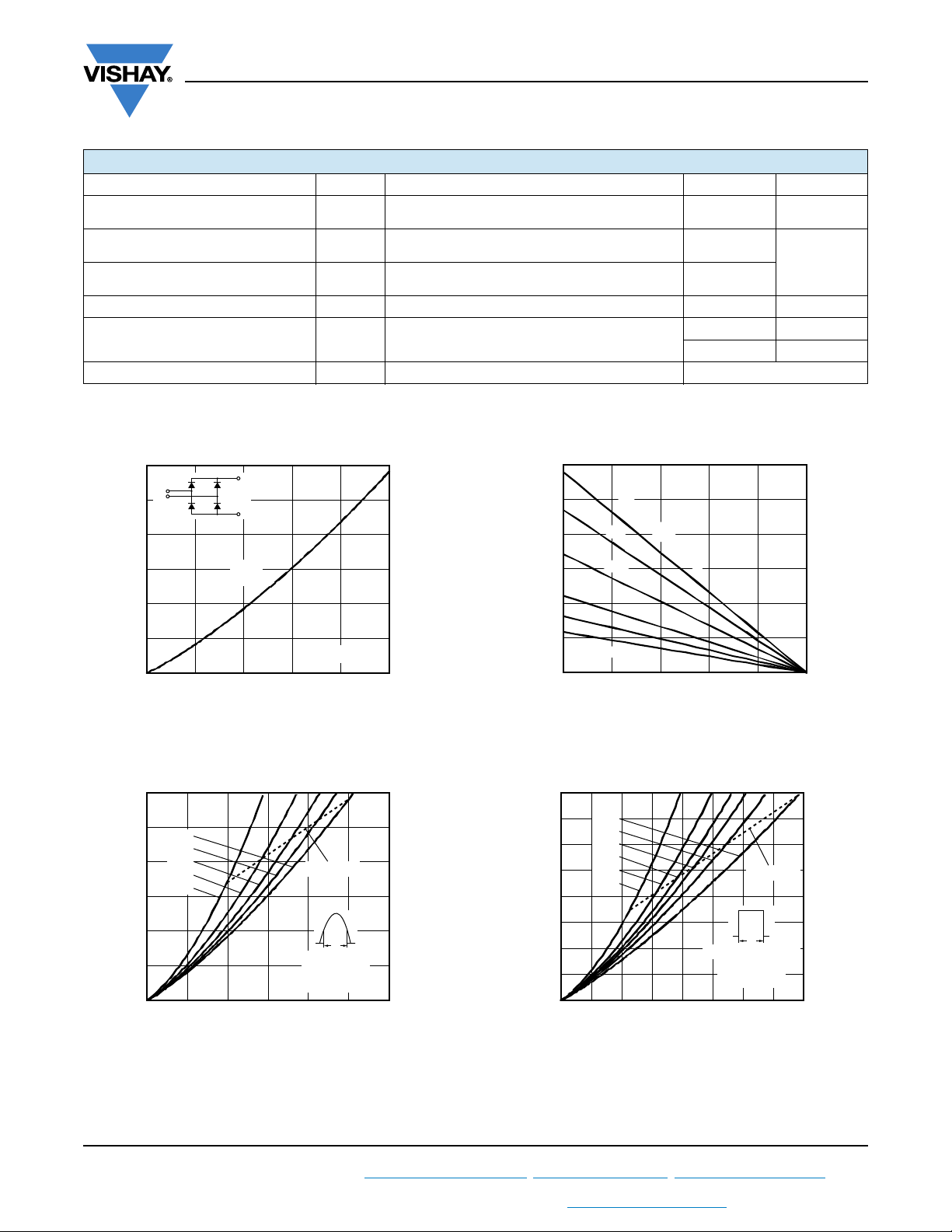
VS-P100 Series
Maximum Average On-State
Power Loss (W)
Average On-State Current (A)
10 1505
15
10
5
0
93754_02
180°
120°
90°
60°
30°
RMS limit
Ø
Conduction angle
TJ = 125 °C
Per junction
Maximum Average On-State
Power Loss (W)
Average On-State Current (A)
20010155
20
10
15
5
0
93754_03
DC
180°
120°
90°
60°
30°
RMS limit
TJ = 125 °C
Per junction
Conduction period
Ø
www.vishay.com
THERMAL AND MECHANICAL SPECIFICATIONS
PARAMETER SYMBOL TEST CONDITIONS VALUES UNITS
Maximum junction operating
and storage temperature range
Maximum thermal resistance,
junction to case per junction
Maximum thermal resistance,
case to heatsink
Mounting torque, base to heatsink
Approximate weight
Case style PACE-PAK (D-19)
Note
(1)
A mounting compound is recommended and the torque should be checked after a period of 3 hours to allow for the spread of the compound
T
, T
J
Stg
R
thJC
R
thCS
(1)
DC operation 2.24
Mounting surface, smooth and greased 0.10
Vishay Semiconductors
-40 to 125 °C
K/W
4Nm
58 g
2.0 oz.
60
~
50
40
30
20
10
+
-
180°
(sine)
Maximum Total Power Loss (W)
0
0
93754_01a
5101520
Total Output Current (A)
60
R
thSA
2 K/W
3 K/W
7 K/W
10 K/W
25 7550 100 125
Maximum Allowable
TJ = 125 °C
50
40
30
5 K/W
20
10
Maximum Total Power Loss (W)
0
25
93754_01b
0
Ambient Temperature (°C)
Fig. 1 - Current Ratings Nomogram (1 Module Per Heatsink)
= 15 K/W - ΔR
Fig. 2 - On-State Power Loss Characteristics Fig. 3 - On-State Power Loss Characteristics
Revision: 27-Mar-14
For technical questions within your region: DiodesAmericas@vishay.com
THIS DOCUMENT IS SUBJECT TO CHANGE WITHOUT NOTICE. THE PRODUCTS DESCRIBED HEREIN AND THIS DOCUMENT
ARE SUBJECT TO SPECIFIC DISCLAIMERS, SET FORTH AT www.vishay.com/doc?91000
3
, DiodesAsia@vishay.com, DiodesEurope@vishay.com
Document Number: 93754
Page 4

www.vishay.com
Maximum Allowable Case
Temperature (°C)
Total Output Current (A)
10 2051525
30
0
70
80
90
100
110
120
130
93754_04
180°
(Sine)
180°
(Rect.)
Fully turned-on
Per module
Instantaneous On-State Current (A)
Instantaneous On-State Voltage (V)
0123456
1
100
10
1000
93754_05
TJ = 25 °C
TJ = 125 °C
Per junction
Peak Half Sine Wave
On-State Current (A)
Number of Equal Amplitude Half
Cycle Current Pulses (N)
10 1001
150
200
300
250
350
93754_06
Per junction
At any rated load condition and with
rated V
RRM
applied following surge.
Initial T
J
= 125 °C
at 60 Hz 0.0083 s
at 50 Hz 0.0100 s
Peak Half Sine Wave
On-State Current (A)
Pulse Train Duration (s)
0.1 10.01
100
150
200
250
300
350
400
93754_07
Maximum non-repetitive surge current
versus pulse train duration. Control of
conduction may not be maintained.
Initial T
J
= 125 °C
No voltage reapplied
Rated V
RRM
reapplied
Per junction
VS-P100 Series
Vishay Semiconductors
Fig. 4 - Current Ratings Characteristics
Fig. 5 - On-State Voltage Drop Characteristics
10
Steady state value
R
= 2.24 K/W
thJC
(DC operation)
1
Fig. 6 - Maximum Non-Repetitive Surge Current
Fig. 7 - Maximum Non-Repetitive Surge Current
0.1
- Transient Thermal
Impedance (K/W)
thJC
Z
Revision: 27-Mar-14
For technical questions within your region: DiodesAmericas@vishay.com
THIS DOCUMENT IS SUBJECT TO CHANGE WITHOUT NOTICE. THE PRODUCTS DESCRIBED HEREIN AND THIS DOCUMENT
0.01
0.0001 0.001 0.01 0.1 101
93754_08
ARE SUBJECT TO SPECIFIC DISCLAIMERS, SET FORTH AT www.vishay.com/doc?91000
Square Wave Pulse Duration (s)
Fig. 8 - Thermal Impedance Z
4
Characteristics
thJC
, DiodesAsia@vishay.com, DiodesEurope@vishay.com
Per junction
Document Number: 93754
Page 5

www.vishay.com
VS-P100 Series
Vishay Semiconductors
100
Rectangular gate pulse
(a) Recommended load line for
10
1
Instantaneous Gate Voltage (V)
0.1
0.001
93754_09
rated dI/dt: 10 V, 20 Ω, t
(b) Recommended load line for
rated dI/dt: 10 V, 65 Ω, t
V
GD
I
GD
r
r
0.01 0.1 1 10 100
ORDERING INFORMATION TABLE
Device code
VS- 1P02KW
(1) PGM = 10 W, tp = 5 ms
(2) P
≤ 1 μs
≤ 1 μs
(b)
T
J
J
= 125 °C
T
T
= 25 °C
J
= 40 °C
(a)
(3) P
(4) P
(1) (2) (3) (4)
Frequency limited by P
Instantaneous Gate Current (A)
Fig. 9 - Gate Characteristics
1 32 4 5 6 7
= 20 W, tp = 25 ms
GM
= 50 W, tp = 1 ms
GM
= 100 W, tp = 500 μs
GM
G(AV)
1 - Vishay Semiconductors product
2 - Module type
- Current rating
3
1 = 25 A DC (P100 Series)
4 = 40 A DC (P400 Series)
- Circuit configuration
4
0 = Single Phase, Hybrid Bridge Common Cathode
2 = Single Phase, Hybrid Bridge Doubler Connection
3 = Single Phase, all SCR Bridge
- Voltage code
5
1 = 400 V
2 = 600 V
3 = 800 V
4 = 1000 V
5 = 1200 V
6 - K = Optional Voltage Suppression
7 - W = Optional Freewheeling Diode
Revision: 27-Mar-14
For technical questions within your region: DiodesAmericas@vishay.com
THIS DOCUMENT IS SUBJECT TO CHANGE WITHOUT NOTICE. THE PRODUCTS DESCRIBED HEREIN AND THIS DOCUMENT
ARE SUBJECT TO SPECIFIC DISCLAIMERS, SET FORTH AT www.vishay.com/doc?91000
5
, DiodesAsia@vishay.com, DiodesEurope@vishay.com
Document Number: 93754
Page 6

www.vishay.com
G1
AC2
AC1
G2
(-) (+)
G1G3
AC2
AC1
(-) (+)
G2G4
AC2
G2-
AC1 G3
G1 G4
+
CIRCUIT CONFIGURATION
CIRCUIT DESCRIPTION
Single phase, hybrid bridge
common cathode
Single phase, hybrid bridge
doubler connection
CONFIGURATION
CIRCUIT
CODE
0
2
VS-P100 Series
Vishay Semiconductors
SCHEMATIC DIAGRAM TERMINAL POSITIONS
AC1
G1-
AC2 G2+
G2G1
AC2
AC1
(-) (+)
AC1
G1-
AC2 G2+
Single phase, all SCR bridge 3
CODING
CIRCUIT DESCRIPTION
Single phase, hybrid bridge
common cathode
Single phase, hybrid bridge
doubler connection
Single phase, all SCR bridge 3
(1)
CIRCUIT
CONFIGURATION
CODE
0
2
BASIC
SERIES
WITH VOLTAGE
SUPPRESSION
P10. P10.K
P12. P12.K
P13. P13.K
WITH
FREEWHEELING
VOLTAGE SUPPRESSION
DIODE
P10.W P10.KW
--
--
Note
(1)
To complete code refer to Voltage Ratings table, i.e.: For 600 V P10.W complete code is P102W
LINKS TO RELATED DOCUMENTS
Dimensions www.vishay.com/doc?95335
WITH BOTH
AND FREEWHEELING
DIODE
Revision: 27-Mar-14
For technical questions within your region: DiodesAmericas@vishay.com
THIS DOCUMENT IS SUBJECT TO CHANGE WITHOUT NOTICE. THE PRODUCTS DESCRIBED HEREIN AND THIS DOCUMENT
6
, DiodesAsia@vishay.com, DiodesEurope@vishay.com
ARE SUBJECT TO SPECIFIC DISCLAIMERS, SET FORTH AT www.vishay.com/doc?91000
Document Number: 93754
Page 7

DIMENSIONS in millimeters (inches)
0.9 x 45°
(0.035 x 45°)
4.6 (0.18)
D-19 PACE-PAK
12.7 (0.50)
12.7 (0.50)
Outline Dimensions
Vishay Semiconductors
Ø 1.65 (0.06)
2.5 (0.10)
MAX.
23.2 (0.91)
63.5 (2.50)
45 (1.77)
33.8 (1.33)
48.7 (1.91)
15.5 (0.61)
MAX.
Fast-on 6.35 x 0.8 (0.25 x 0.03)
5.2 (0.20)
25 (0.98) MAX.
32.5 (1.28) MAX.
Document Number: 95335 For technical questions, contact: indmodules@vishay.com
Revision: 24-Jul-08 1
www.vishay.com
Page 8

Legal Disclaimer Notice
www.vishay.com
Vishay
Disclaimer
ALL PRODUCT, PRODUCT SPECIFICATIONS AND DATA ARE SUBJECT TO CHANGE WITHOUT NOTICE TO IMPROVE
RELIABILITY, FUNCTION OR DESIGN OR OTHERWISE.
Vishay Intertechnology, Inc., its affiliates, agents, and employees, and all persons acting on its or their behalf (collectively,
“Vishay”), disclaim any and all liability for any errors, inaccuracies or incompleteness contained in any datasheet or in any other
disclosure relating to any product.
Vishay makes no warranty, representation or guarantee regarding the suitability of the products for any particular purpose or
the continuing production of any product. To the maximum extent permitted by applicable law, Vishay disclaims (i) any and all
liability arising out of the application or use of any product, (ii) any and all liability, including without limitation special,
consequential or incidental damages, and (iii) any and all implied warranties, including warranties of fitness for particular
purpose, non-infringement and merchantability.
Statements regarding the suitability of products for certain types of applications are based on Vishay’s knowledge of typical
requirements that are often placed on Vishay products in generic applications. Such statements are not binding statements
about the suitability of products for a particular application. It is the customer’s responsibility to validate that a particular
product with the properties described in the product specification is suitable for use in a particular application. Parameters
provided in datasheets and/or specifications may vary in different applications and performance may vary over time. All
operating parameters, including typical parameters, must be validated for each customer application by the customer’s
technical experts. Product specifications do not expand or otherwise modify Vishay’s terms and conditions of purchase,
including but not limited to the warranty expressed therein.
Except as expressly indicated in writing, Vishay products are not designed for use in medical, life-saving, or life-sustaining
applications or for any other application in which the failure of the Vishay product could result in personal injury or death.
Customers using or selling Vishay products not expressly indicated for use in such applications do so at their own risk. Please
contact authorized Vishay personnel to obtain written terms and conditions regarding products designed for such applications.
No license, express or implied, by estoppel or otherwise, to any intellectual property rights is granted by this document or by
any conduct of Vishay. Product names and markings noted herein may be trademarks of their respective owners.
Material Category Policy
Vishay Intertechnology, Inc. hereby certifies that all its products that are identified as RoHS-Compliant fulfill the
definitions and restrictions defined under Directive 2011/65/EU of The European Parliament and of the Council
of June 8, 2011 on the restriction of the use of certain hazardous substances in electrical and electronic equipment
(EEE) - recast, unless otherwise specified as non-compliant.
Please note that some Vishay documentation may still make reference to RoHS Directive 2002/95/EC. We confirm that
all the products identified as being compliant to Directive 2002/95/EC conform to Directive 2011/65/EU.
Vishay Intertechnology, Inc. hereby certifies that all its products that are identified as Halogen-Free follow Halogen-Free
requirements as per JEDEC JS709A standards. Please note that some Vishay documentation may still make reference
to the IEC 61249-2-21 definition. We confirm that all the products identified as being compliant to IEC 61249-2-21
conform to JEDEC JS709A standards.
Revision: 02-Oct-12
1
Document Number: 91000
 Loading...