

Page 1
PRODUCT SUMMARY
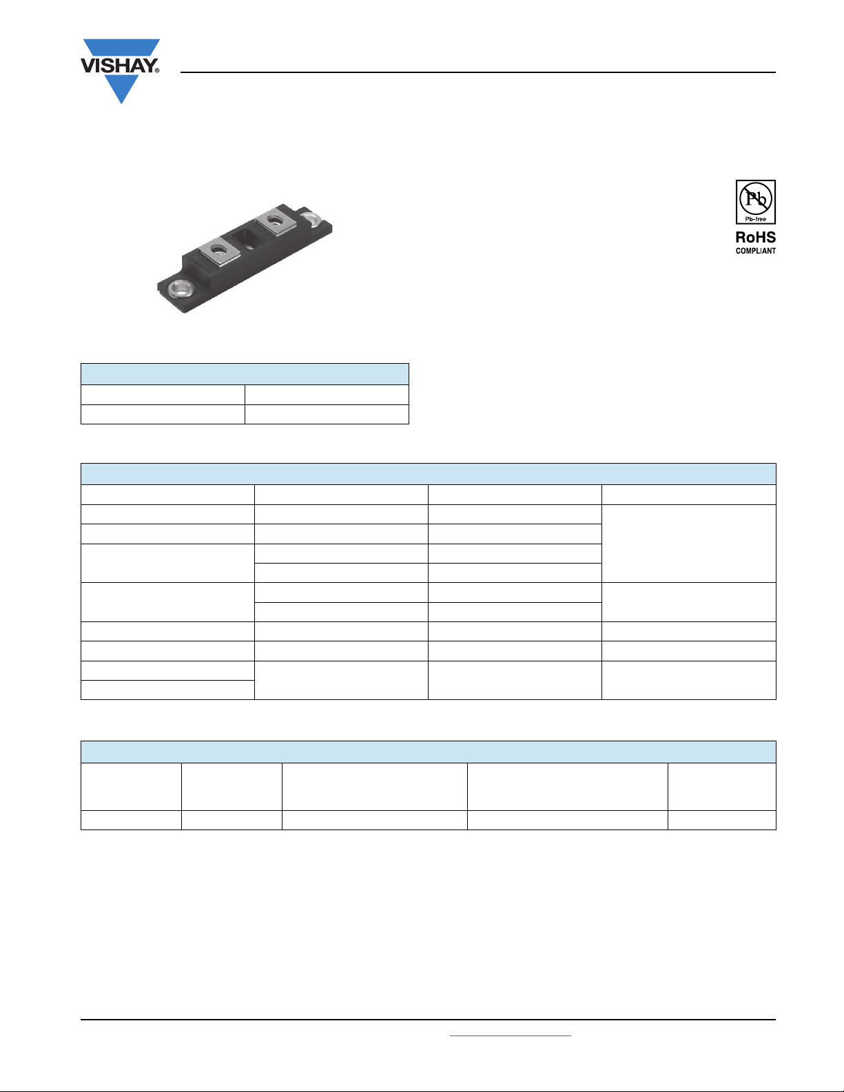
TO-244
I
per module 400 A
F(AV)
Type Modules - Diode, High Voltage
Preliminary
VSMD400AW60, VSMD400CW60
Vishay Semiconductors
Standard Recovery Diodes, 400 A
FEATURES
• Standard rectifier
• Popular series for rough service
• Cathode and anode to base available
• Compliant to RoHS Directive 2002/95/EC
• Designed and qualified for industrial level
TYPICAL APPLICATIONS
• Welders
• Power supplies
• Motor controls
• Battery chargers
• General industrial current rectification
MAJOR RATINGS AND CHARACTERISTICS
SYMBOL CHARACTERISTICS VALUES UNITS
I
F(AV)
I
F(RMS)
I
FSM
2
I
t
2
I
√t 312 kA2√s
V
RRM
T
J
T
Stg
133 °C 400
628
50 Hz 2500
60 Hz 2620
50 Hz 31
60 Hz 28
600 V
- 40 to 175 °C
A
kA2s
ELECTRICAL SPECIFICATIONS
VOLTAGE RATINGS
V
, MAXIMUM REPETITIVE
TYPE NUMBER
VSMD400.W60 60 600 700 12
VOLTAGE
CODE
RRM
PEAK REVERSE VOLTAGE
V
V
, MAXIMUM NON-REPETITIVE
RSM
PEAK REVERSE VOLTAGE
V
I
RRM
AT T
MAXIMUM
= 175 °C
J
mA
Document Number: 93469 For technical questions, contact: indmodules@vishay.com
Revision: 21-Dec-10 1
www.vishay.com
Page 2
Preliminary
VSMD400AW60, VSMD400CW60
Vishay Semiconductors
Standard Recovery Diodes, 400 A
FORWARD CONDUCTION
PARAMETER SYMBOL TEST CONDITIONS VALUES UNITS
Maximum average forward current at case
temperature per leg
Maximum RMS forward current per leg I
Maximum peak, one-cycle forward,
non-repetitive surge current per leg
2
Maximum I
Maximum I
t for fusing per leg I2t
2
√t for fusing per leg I2√t t = 0.1 ms to 10 ms, no voltage reapplied 311 kA2√s
Low level value of threshold voltage per leg V
High level value of threshold voltage per leg V
Low level value of forward
slope resistance per leg
High level value of forward
slope resistance per leg
Maximum forward voltage drop per leg V
I
F(AV)
F(RMS)
I
FSM
F(TO)1
F(TO)2
r
f1
r
f2
FM
180° conduction, half sine wave
DC at 137 °C case temperature 314
t = 10 ms
t = 8.3 ms 2620
t = 10 ms
t = 8.3 ms 2200
t = 10 ms
t = 8.3 ms 29
t = 10 ms
t = 8.3 ms 20
(16.7 % x π x I
(I > π x I
(16.7 % x π x I
(I > π x I
No voltage
reapplied
100 % V
RRM
reapplied
No voltage
Sinusoidal half wave,
= TJ maximum
initial T
J
reapplied
100 % V
RRM
reapplied
< I < π x I
F(AV)
), TJ = TJ maximum 0.85
F(AV)
< I < π x I
F(AV)
), TJ = TJ maximum 1.36
F(AV)
), TJ = TJ maximum 0.73
F(AV)
), TJ = TJ maximum 1.52
F(AV)
IFM = 200 A, TJ = 25 °C, tp = 400 μs square wave 1.31 V
200 A
133 °C
2500
2100
32
22
A
kA2s
V
mΩ
BLOCKING
PARAMETER SYMBOL TEST CONDITIONS VALUES UNITS
Maximum peak reverse leakage
current per module
I
RRM
TJ = 175 °C 12 mA
THERMAL AND MECHANICAL SPECIFICATIONS
PARAMETER SYMBOL MIN. TYP. MAX. UNITS
Thermal resistance,
junction to case
Thermal resistance,
case to heatsink per module
per leg
per module - - 0.05
R
thJC
R
thCS
Weight
Mounting torque 30 (3.4) - 40 (4.6)
Mounting torque center hole 12 (1.4) - 18 (2.1)
Terminal torque 30 (3.4) - 40 (4.6)
Vertical pull - - 80
2” lever pull - - 35
- - 0.10
°C/W
-0.10-
-68- g
-2.4-oz.
lbf · in
(N · m)
lbf · in
Case style TO-244
ΔR CONDUCTION PER JUNCTION
DEVICES
VSMD400.W60 0.041 0.047 0.060 0.084 0.131 0.029 0.049 0.064 0.087 0.132 °C/W
Note
• Table shows the increment of thermal resistance R
www.vishay.com For technical questions, contact: indmodules@vishay.com
2 Revision: 21-Dec-10
SINE HALF WAVE CONDUCTION RECTANGULAR WAVE CONDUCTION
180° 120° 90° 60° 30° 180° 120° 90° 60° 30°
when devices operate at different conduction angles than DC
thJC
Document Number: 93469
UNITS
Page 3

Preliminary
Maximum Allowable Case
Temperature (°C)
Average Forward Current Per Leg (A)
40 80 120 160 200
220
0
110
130
150
180
100
120
140
170
160
90
Conduction angle
Ø
30°
60°
90°
120°
180°
Maximum Allowable Case
Temperature (°C)
Average Forward Current Per Leg (A)
20015010050 250 300
350
0
120
140
160
180
90
100
130
150
170
110
Ø
Conduction angle
30°
60°
90°
120°
180°
DC
Maximum Average On-State
Power Loss (W)
Average Forward Current Per Leg (A)
40 80 120
160 200
0
0
350
300
250
200
150
50
100
RMS limit
180°
120°
90°
60°
30°
Conduction angle
Ø
VSMD400AW60, VSMD400CW60
Standard Recovery Diodes, 400 A
Fig. 1 - Current Ratings Characteristics Per Leg
Fig. 2 - Current Ratings Characteristics Per Leg
Vishay Semiconductors
2500
2300
2100
1900
1700
1500
1300
1100
Forward Current (A)
Peak Half Sine Wave
900
700
500
1
Number of Equal Amplitude Half
Cycle Current Pulses (N)
Fig. 3 - Maximum Non-Repetitive Surge Current Per Leg
2500
2300
2100
1900
1700
1500
1300
1100
Forward Current (A)
Peak Half Sine Wave
900
700
500
Rated V
0.01
No voltage reapplied
reapplied
RRM
Pulse Train Duration (s)
Fig. 4 - Maximum Non-Repetitive Surge Current Per Leg
10
60 Hz 0.0083 s
50 Hz 0.0100 s
100
10.1
Document Number: 93469 For technical questions, contact: indmodules@vishay.com
Revision: 21-Dec-10 3
350
300
250
200
150
Power Loss (W)
100
Maximum Average On-State
0.7 °C/W
1 °C/W
1.5 °C/W
3 °C/W
50
0
0
25 50 75 125 175100 150 200
Fig. 5 - Forward Power Loss Characteristics
0.5 °C/W
thSA
= 0.1 °C/W
R
0.3 °C/W
Maximum Allowable Ambient
Temperature (°C)
www.vishay.com
Page 4

Preliminary
Maximum On-State Forward
Power Loss (W)
Average Forward Current Per Leg (A)
40 80 160
240
120 200
280 320
0
0
450
350
300
400
250
200
150
50
100
180°
120°
90°
60°
30°
RMS limit
Ø
Conduction angle
DC
Instantaneous Forward Current (A)
Instantaneous Forward Voltage (V)
0 0.5 1.0 1.5 2.0 2.5 3.0
1
10
1000
100
TJ = 175 °C
TJ = 25 °C
0.001 0.001 0.1 101
Square Wave Pulse Duration (s)
Z
thJC
- Transient Thermal
Impedance (°C/W)
0.01
0.1
1
VSMD400..W60
Steady state value
R
thJC
= 0.10 °C/W
0.001
VSMD400AW60, VSMD400CW60
Vishay Semiconductors
Standard Recovery Diodes, 400 A
450
400
350
300
250
200
150
Power Loss (W)
100
Maximum Average On-State
50
0
Fig. 6 - Forward Power Loss Characteristics
0.3 °C/W
0.5 °C/W
0.7 °C/W
1 °C/W
3 °C/W
0
20 40 60 100 14080 120 160
Maximum Allowable Ambient
R
thSA
0.2 °C/W
= 0.1 °C/W
Temperature (°C)
Fig. 7 - Forward Voltage Drop Characteristics Per Leg
www.vishay.com For technical questions, contact: indmodules@vishay.com
4 Revision: 21-Dec-10
Fig. 8 - Thermal Impedance Z
Characteristics Per Leg
thJC
Document Number: 93469
Page 5

Preliminary
Base common cathode
Lug
terminal
anode 2
Lug
terminal
anode 1
VSMD400AW60, VSMD400CW60
Standard Recovery Diodes, 400 A
ORDERING INFORMATION TABLE
Device code
1
2
3
4
5
6
VS MD 400 C W 60
1
32 4 6
- Vishay Semiconductors product
- MD = Standard recovery diode
- Current rating (400 = 400 A)
- Circuit configuration:
C = Common cathode
A = Common anode
- Type of device:
W = TO-244 not isolated
- Voltage rating (60 = 600 V)
5
Vishay Semiconductors
CIRCUIT CONFIGURATION
CIRCUIT DESCRIPTION CIRCUIT CONFIGURATION CODE CIRCUIT DRAWING
Lug
terminal
cathode 1
Common anode A
Base common cathode
Common cathode C
Lug
terminal
cathode 2
Document Number: 93469 For technical questions, contact: indmodules@vishay.com
Revision: 21-Dec-10 5
www.vishay.com
Page 6

Preliminary
3
2
3
1
Ø 5.2 (Ø 0.20)
9.6 (0.37) MIN.
93 (3.66) MAX.
¼" - 20 UNC
80 (3.15)
13 (0.51)
35 (1.37) REF.
7 (0.27)
6 (0.23)
17.5 (0.69)
16.5 (0.65)
21 (0.82)
20 (0.78)
Ø 7.2 (Ø 0.28)
(2 places)
12.6 (0.5)
VSMD400AW60, VSMD400CW60
Vishay Semiconductors
DIMENSIONS in millimeters (inches)
Standard Recovery Diodes, 400 A
www.vishay.com For technical questions, contact: indmodules@vishay.com
6 Revision: 21-Dec-10
Document Number: 93469
 Loading...