

Page 1
www.vishay.com
D-34
PRODUCT SUMMARY
I
O
V
RRM
Package D-34
Circuit Single Phase Bridge
Single Phase Bridge
(Power Modules), 25 A/35 A
FEATURES
• Universal, 3 way terminals:
Push-on, wrap around or solder
• High thermal conductivity package, electrically
insulated case
• Center hole fixing
• Excellent power/volume ratio
• UL E300359 approved
• Nickel plated terminals solderable using lead (Pb)-free
solder; Solder Alloy Sn/Ag/Cu (SAC305); Solder
temperature 260 °C to 275 °C
• Designed and qualified for industrial level
• Material categorization: For definitions of compliance
please see www.vishay.com/doc?99912
25 A to 35 A
200 V to 1200 V
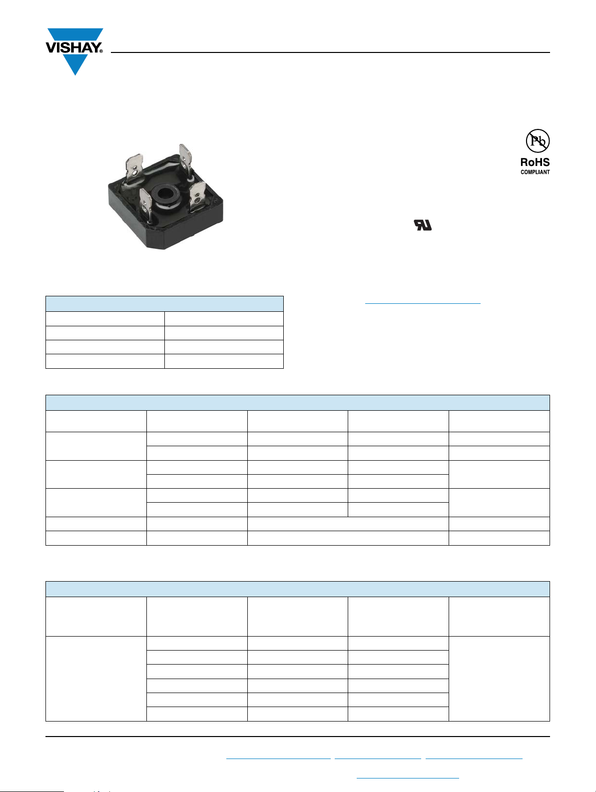
DESCRIPTION
A range of extremely compact, encapsulated single phase
bridge rectifiers offering efficient and reliable operation.
They are intended for use in general purpose and
instrumentation applications.
VS-MB Series
Vishay Semiconductors
MAJOR RATINGS AND CHARACTERISTICS
SYMBOL CHARACTERISTICS
I
O
I
FSM
2
I
V
T
t
RRM
J
T
C
50 Hz 400 475
60 Hz 420 500
50 Hz 790 1130
60 Hz 725 1030
Range 200 to 1200 V
ELECTRICAL SPECIFICATIONS
VOLTAGE RATINGS
TYPE NUMBER
26MB..A
36MB..A
VOLTAGE
CODE
20 200 275
40 400 500
60 600 725
80 800 900
100 1000 1100
120 1200 1300
VALUES
26MB-A
25 35 A
65 60 °C
, MAXIMUM
V
RRM
REPETITIVE PEAK
REVERSE VOLTAGE
V
VALUES
36MB-A
- 55 to 150 °C
V
, MAXIMUM
RSM
NON-REPETITIVE PEAK
REVERSE VOLTAGE
V
I
RRM
AT T
UNITS
A2s
MAXIMUM
MAXIMUM
J
A
2
Revision: 10-Jul-13
For technical questions within your region: DiodesAmericas@vishay.com
THIS DOCUMENT IS SUBJECT TO CHANGE WITHOUT NOTICE. THE PRODUCTS DESCRIBED HEREIN AND THIS DOCUMENT
ARE SUBJECT TO SPECIFIC DISCLAIMERS, SET FORTH AT www.vishay.com/doc?91000
1
, DiodesAsia@vishay.com, DiodesEurope@vishay.com
Document Number: 93563
Page 2
www.vishay.com
Vishay Semiconductors
FORWARD CONDUCTION
PARAMETER SYMBOL TEST CONDITIONS
Resistive or inductive load 25 35
Maximum DC output current
at case temperature
Maximum peak, one-cycle
non-repetitive forward current
Maximum I
Maximum I
2
t for fusing I2t
2
t for fusing I2tI2t for time tx = I2xx0.1 tx 10 ms, V
Low level value of threshold voltage V
High level value of threshold voltage V
Low level forward slope resistance r
High level forward slope resistance r
Maximum forward voltage drop V
Maximum DC reverse current I
RMS isolation voltage base plate V
I
I
FSM
F(TO)1
F(TO)2
RRM
Capacitive load 20 28
O
t = 10 ms
t = 8.3 ms 420 500
t = 10 ms
t = 8.3 ms 350 420
t = 10 ms
t = 8.3 ms 725 1030
t = 10 ms
t = 8.3 ms 512 730
(16.7 % x x I
(I > x I
(16.7 % x x I
t1
(I > x I
t2
TJ = 25 °C, IFM = 40 Apk (26MB)
FM
T
= 25 °C, IFM = 55 Apk (36MB)
J
TJ = 25 °C, per diode at V
f = 50 Hz, t = 1 s 2700 V
INS
No voltage
reapplied
100 % V
reapplied
No voltage
RRM
Initial
T
= TJ maximum
J
reapplied
100 % V
reapplied
F(AV)
), TJ maximum 0.92 0.96
F(AV)
F(AV)
), TJ maximum 5.0 4.5
F(AV)
RRM
< I < x I
< I < x I
RRM
= 0 V 5.6 11.3 kA2s
RRM
), TJ maximum 0.76 0.79
F(AV)
), TJ maximum 6.8 5.8
F(AV)
t
= 400 μs 1.11 1.14 V
p
VALUES
26MB-A
VS-MB Series
VALUES
36MB-A
65 60 °C
400 475
335 400
790 1130
560 800
10 μA
UNITS
A2s
m
A
A
V
THERMAL AND MECHANICAL SPECIFICATIONS
PARAMETER SYMBOL TEST CONDITIONS
Junction and storage temperature
range
Maximum thermal resistance
junction to case per bridge
Maximum thermal resistance,
case to heatsink
T
, T
J
Stg
R
thJC
R
thCS
Mounting surface, smooth, flat and greased 0.2
VALUES
26MB-A
1.7 1.2
Approximate weight 20 g
Mounting torque ± 10 % Bridge to heatsink 2.0 Nm
Revision: 10-Jul-13
For technical questions within your region: DiodesAmericas@vishay.com
2
, DiodesAsia@vishay.com, DiodesEurope@vishay.com
THIS DOCUMENT IS SUBJECT TO CHANGE WITHOUT NOTICE. THE PRODUCTS DESCRIBED HEREIN AND THIS DOCUMENT
ARE SUBJECT TO SPECIFIC DISCLAIMERS, SET FORTH AT www.vishay.com/doc?91000
VALUES
36MB-A
- 55 to 150 °C
Document Number: 93563
UNITS
K/W
Page 3
www.vishay.com
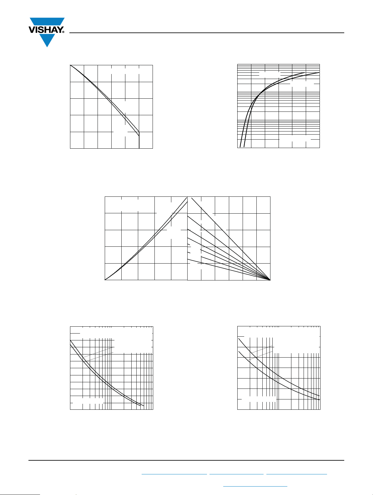
Average Forward Current (A)
Maximum Allowable Case temperature (°C)
50
70
90
110
130
150
0 5 10 15 20 25 30
180°
(Rect)
180°
(Sine)
26MB..A Series
Average Forward Current (A) Maximum Allowable Ambient Temperature (°C)
0
10
20
30
40
50
0 5 10 15 20 25
180°
(Sine)
26MB..A Series
T
J
= 150 °C
180°
(Rect)
Maximum Average Forward Power Loss (W)
Number of Equal Amplitude Half Cycle Current Pulses (N)
Peak Half Sine Wave Forward Current (A)
100
150
200
250
300
350
400
110100
26MB..A Series
At Any Rated Load Condition And With
Initial TJ = 150 °C
at 60 Hz 0.0083 s
at 50 Hz 0.0100 s
Rated V
RRM
Applied Following Surge
VS-MB Series
Vishay Semiconductors
1000
Tj = 25 °C
Tj = 150 °C
100
10
Instantaneous Forward Current (A)
1
0.5 1 1.5 2 2.5 3 3.5
Instantaneous Forward Voltage (V)
26MB..A Series
Fig. 1 - Current Ratings Characteristics Fig. 2 - Forward Voltage Drop Characteristics
Maximum Allowable Ambient Temperature
RthSA = 1 K/W - Δ R
2 K/W
3 K/W
4 K/W
5 K/W
7 K/W
10 K/W
0 25 50 75 100 125 150
Fig. 3 - Total Power Loss Characteristics
Fig. 4 - Maximum Non-Repetitive Surge Current Fig. 5 - Maximum Non-Repetitive Surge Current
Revision: 10-Jul-13
For technical questions within your region: DiodesAmericas@vishay.com
THIS DOCUMENT IS SUBJECT TO CHANGE WITHOUT NOTICE. THE PRODUCTS DESCRIBED HEREIN AND THIS DOCUMENT
ARE SUBJECT TO SPECIFIC DISCLAIMERS, SET FORTH AT www.vishay.com/doc?91000
450
350
Maximum Non Repetitive Surge Current
Versus Pulse Train Duration.
Initial TJ = 150 °C
No Voltage Reapplied
Rated V
Reapplied
RRM
250
150
26MB..A Series
50
Peak Half Sine Wave Forward Current (A)
0.01 0.1 1
3
Pulse Train Duration (s)
Document Number: 93563
, DiodesAsia@vishay.com, DiodesEurope@vishay.com
Page 4

VS-MB Series
Instantaneous Forward Voltage (V)
Instantaneous Forward Current (A)
1
10
100
1000
0.5 1 1.5 2 2.5 3 3.5
TJ = 25 °C
TJ = 150 °C
36MB..A Series
Average Forward Current (A)
Maximum Average Forward Power Loss (W)
Maximum Allowable Ambient Temperature (°C)
35 25 50 75 100 125 15
0
1 K/W
2 K/W
3 K/W
4 K/W
5 K/W
7 K/W
RthSA = 0.7 K/W - Delta R
0
20
40
60
80
0 5 10 15 20 25 30
180°
(Sine)
180°
(Rect)
36MB..A Series
T
J
= 150 °C
Number of Equal Amplitude Half Cycle Current Pulses (N)
Peak Half Sine Wave Forward Current (A)
100
150
200
250
300
350
400
450
110100
At Any Rated Load Condition And With
Rated V
RRM
Applied Following Surge.
Initial TJ = 150 °C
at 60 Hz 0.0083 s
at 50 Hz 0.0100 s
36MB..A Series
www.vishay.com
150
36MB..A Series
130
110
180°
90
70
50
Maximum Allowable Case temperature (°C)
0 5 10 15 20 25 30 35 40
Average Forward Current (A)
Fig. 6 - Current Ratings Characteristics Fig. 7 - Forward Voltage Drop Characteristics
(Rect)
180°
(Sine)
Vishay Semiconductors
Revision: 10-Jul-13
Fig. 9 - Maximum Non-Repetitive Surge Current Fig. 10 - Maximum Non-Repetitive Surge Current
For technical questions within your region: DiodesAmericas@vishay.com
THIS DOCUMENT IS SUBJECT TO CHANGE WITHOUT NOTICE. THE PRODUCTS DESCRIBED HEREIN AND THIS DOCUMENT
ARE SUBJECT TO SPECIFIC DISCLAIMERS, SET FORTH AT www.vishay.com/doc?91000
Fig. 8 - Total Power Loss Characteristics
500
450
400
350
300
250
200
150
100
Peak Half Sine Wave Forward Current (A)
4
, DiodesAsia@vishay.com, DiodesEurope@vishay.com
Maximum Non Repetitive Surge Current
Versus Pulse Train Duration.
Initial TJ = 150 °C
No Voltage Reapplied
Rated V
Reapplied
RRM
36MB..A Series
0.01 0.1 1
Pulse Train Duration (s)
Document Number: 93563
Page 5

www.vishay.com
(+)
AC
AC
(-)
ORDERING INFORMATION TABLE
VS-MB Series
Vishay Semiconductors
Device code
CIRCUIT CONFIGURATION
36VS- MB 120 A
1
1
- Vishay Semiconductors product
2
- Current rating code
3
- Circuit configuration:
- Voltage code x 10 = V
4
- Diode bridge rectifier:
5
32 4 5
MB = Single phase european coding
A = 26 MB, 36 MB series
26 = 25 A (average)
36 = 35 A (average)
RRM
LINKS TO RELATED DOCUMENTS
Dimensions www.vishay.com/doc?95326
Revision: 10-Jul-13
For technical questions within your region: DiodesAmericas@vishay.com
THIS DOCUMENT IS SUBJECT TO CHANGE WITHOUT NOTICE. THE PRODUCTS DESCRIBED HEREIN AND THIS DOCUMENT
ARE SUBJECT TO SPECIFIC DISCLAIMERS, SET FORTH AT www.vishay.com/doc?91000
5
, DiodesAsia@vishay.com, DiodesEurope@vishay.com
Document Number: 93563
Page 6

DIMENSIONS in millimeters (inches)
Outline Dimensions
Vishay Semiconductors
D-34
+ 1.0
21.5
- 0.5
+ 0.039
(0.85 )
- 0.020
9.5 ± 0.5
(0.37 ± 0.020)
Not to scale
0.8 ± 0.05
(0.03 ± 0.002)
-
~
5.25 ± 0.15
(0.21 ± 0.006)
6.35 ± 0.1
(0.25 ± 0.004)
10.5 ± 0.15
(0.41 ± 0.006)
20.3 ± 0.15
(0.80 ± 0.006)
~
28.5 ± 0.15
(1.12 ± 0.006)
12.7 ± 0.1
(0.5 ± 0.004)
+
12.7 ± 0.1
(0.5 ± 0.004)
28.5 ± 0.15
(1.12 ± 0.006)
200 N max; axially applied to fast-on terminals
Document Number: 95326 For technical questions, contact: indmodules@vishay.com
Revision: 07-Jul-08 1
Suggested plugging force:
www.vishay.com
Page 7

Legal Disclaimer Notice
www.vishay.com
Vishay
Disclaimer
ALL PRODUCT, PRODUCT SPECIFICATIONS AND DATA ARE SUBJECT TO CHANGE WITHOUT NOTICE TO IMPROVE
RELIABILITY, FUNCTION OR DESIGN OR OTHERWISE.
Vishay Intertechnology, Inc., its affiliates, agents, and employees, and all persons acting on its or their behalf (collectively,
“Vishay”), disclaim any and all liability for any errors, inaccuracies or incompleteness contained in any datasheet or in any other
disclosure relating to any product.
Vishay makes no warranty, representation or guarantee regarding the suitability of the products for any particular purpose or
the continuing production of any product. To the maximum extent permitted by applicable law, Vishay disclaims (i) any and all
liability arising out of the application or use of any product, (ii) any and all liability, including without limitation special,
consequential or incidental damages, and (iii) any and all implied warranties, including warranties of fitness for particular
purpose, non-infringement and merchantability.
Statements regarding the suitability of products for certain types of applications are based on Vishay’s knowledge of typical
requirements that are often placed on Vishay products in generic applications. Such statements are not binding statements
about the suitability of products for a particular application. It is the customer’s responsibility to validate that a particular
product with the properties described in the product specification is suitable for use in a particular application. Parameters
provided in datasheets and/or specifications may vary in different applications and performance may vary over time. All
operating parameters, including typical parameters, must be validated for each customer application by the customer’s
technical experts. Product specifications do not expand or otherwise modify Vishay’s terms and conditions of purchase,
including but not limited to the warranty expressed therein.
Except as expressly indicated in writing, Vishay products are not designed for use in medical, life-saving, or life-sustaining
applications or for any other application in which the failure of the Vishay product could result in personal injury or death.
Customers using or selling Vishay products not expressly indicated for use in such applications do so at their own risk. Please
contact authorized Vishay personnel to obtain written terms and conditions regarding products designed for such applications.
No license, express or implied, by estoppel or otherwise, to any intellectual property rights is granted by this document or by
any conduct of Vishay. Product names and markings noted herein may be trademarks of their respective owners.
Material Category Policy
Vishay Intertechnology, Inc. hereby certifies that all its products that are identified as RoHS-Compliant fulfill the
definitions and restrictions defined under Directive 2011/65/EU of The European Parliament and of the Council
of June 8, 2011 on the restriction of the use of certain hazardous substances in electrical and electronic equipment
(EEE) - recast, unless otherwise specified as non-compliant.
Please note that some Vishay documentation may still make reference to RoHS Directive 2002/95/EC. We confirm that
all the products identified as being compliant to Directive 2002/95/EC conform to Directive 2011/65/EU.
Vishay Intertechnology, Inc. hereby certifies that all its products that are identified as Halogen-Free follow Halogen-Free
requirements as per JEDEC JS709A standards. Please note that some Vishay documentation may still make reference
to the IEC 61249-2-21 definition. We confirm that all the products identified as being compliant to IEC 61249-2-21
conform to JEDEC JS709A standards.
Revision: 02-Oct-12
1
Document Number: 91000
 Loading...