

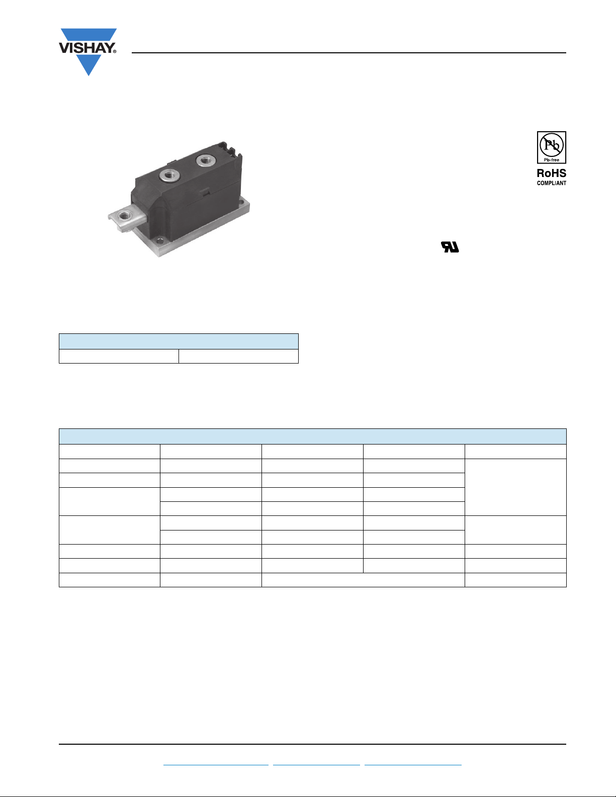
(MAGN-A-PAK Power Modules), 170 A/250 A
MAGN-A-PAK
PRODUCT SUMMARY
I
T(AV)
VSK.170PbF, VSK.250PbF Series
SCR/SCR and SCR/Diode
FEATURES
• High voltage
• Electrically isolated base plate
170 A/250 A
• 3500 V
• Industrial standard package
• Simplified mechanical designs, rapid assembly
• High surge capability
• Large creepage distances
• UL approved file E78996
• Compliant to RoHS directive 2002/95/EC
• Designed and qualified for industrial level
DESCRIPTION
This new VSK series of MAGN-A-PAK modules uses high
voltage power thyristor/thyristor and thyristor/diode in
seven basic configurations. The semiconductors are
electrically isolated from the metal base, allowing common
heatsinks and compact assemblies to be built. They can be
interconnected to form single phase or three phase bridges
or as AC-switches when modules are connected in
anti-parallel mode. These modules are intended for general
purpose applications such as battery chargers, welders,
motor drives, UPS, etc.
isolating voltage
RMS
Vishay Semiconductors
MAJOR RATINGS AND CHARACTERISTICS
SYMBOL CHARACTERISTICS VSK.170.. VSK.250.. UNITS
I
T(AV)
I
T(RMS)
I
TSM
2
t
I
2
I
t 1310 3610 kA2s
V
DRM/VRRM
T
J
85 °C 170 250
377 555
50 Hz 5100 8500
60 Hz 5350 8900
50 Hz 131 361
60 Hz 119 330
Up to 1600 Up to 2000 V
Range - 40 to 130 °C
kA2s
A
Document Number: 94417 For technical questions within your region, please contact one of the following: www.vishay.com
Revision: 02-Jul-10 DiodesAmericas@vishay.com
, DiodesAsia@vishay.com, DiodesEurope@vishay.com 1
VSK.170PbF, VSK.250PbF Series
Vishay Semiconductors
ELECTRICAL SPECIFICATIONS
VOLTAGE RATINGS
V
TYPE NUMBER
VSK.170-
VSK.250-
VOLTAGE
CODE
04 400 500
08 800 900
10 1000 1100
12 1200 1300
14 1400 1500
16 1600 1700
04 400 500
08 800 900
10 1000 1100
12 1200 1300
14 1400 1500
16 1600 1700
18 1800 1900
20 2000 2100
SCR/SCR and SCR/Diode
(MAGN-A-PAK Power Modules), 170 A/250 A
RRM/VDRM
, MAXIMUM REPETITIVE
PEAK REVERSE AND OFF-STATE
BLOCKING VOLTAGE
V
V
, MAXIMUM
RSM
NON-REPETITIVE PEAK
REVERSE VOLTAGE
V
I
RRM/IDRM
AT 130 °C
MAXIMUM
mA
50
50
60
ON-STATE CONDUCTION
PARAMETER SYMBOL TEST CONDITIONS VSK.170 VSK.250 UNITS
Maximum average on-state current
at case temperature
Maximum RMS on-state current I
Maximum peak, one-cycle on-state
non-repetitive, surge current
2
Maximum I
Maximum I
t for fusing I2t
2
t for fusing I2t t = 0.1 ms to 10 ms, no voltage reapplied 1310 3610 kA2s
Low level value or threshold voltage V
High level value of threshold voltage V
Low level value on-state slope resistance r
High level value on-state slope resistance r
Maximum on-state voltage drop V
Maximum holding current I
Maximum latching current I
I
T(AV)
T(RMS)
I
TSM
T(TO)1
T(TO)2
t1
(I > x I
t2
TM
H
L
180° conduction, half sine wave
As AC switch 377 555
t = 10 ms
t = 8.3 ms 5350 8900
t = 10 ms
t = 8.3 ms 4500 7500
t = 10 ms
t = 8.3 ms 119 330
t = 10 ms
t = 8.3 ms 84.4 233
(16.7 % x x I
T
= TJ maximum
J
(I > x I
T(AV)
(16.7 % x x I
T
= TJ maximum
J
T(AV)
ITM = x I
T(AV)
average power = V
No voltage
reapplied
100 % V
reapplied
No voltage
reapplied
100 % V
RRM
RRM
Sinusoidal
half wave,
initial T
=
J
maximum
T
J
reapplied
< I < x I
T(AV)
< I < x I
< I < x I
T(AV)
< I < x I
T(AV)
T(AV)
),
T(AV)
), TJ = TJ maximum 1.12 1.00
),
T(AV)
), TJ = TJ maximum 0.96 0.57
, TJ = TJ maximum, 180° conduction,
T(TO)
x I
T(AV)
+ rf x (I
T(RMS)
2
)
Anode supply = 12 V, initial IT = 30 A, TJ = 25 °C 500 500
Anode supply = 12 V, resistive load = 1 ,
gate pulse: 10 V, 100 μs, T
= 25 °C
J
www.vishay.com For technical questions within your region, please contact one of the following: Document Number: 94417
2 DiodesAmericas@vishay.com
, DiodesAsia@vishay.com, DiodesEurope@vishay.com Revision: 02-Jul-10
170 250 A
85 85 °C
5100 8500
4300 7150
131 361
92.5 255
kA2s
0.89 0.97
1.34 0.60
1.60 1.44 V
1000 1000
A
V
m
mA
VSK.170PbF, VSK.250PbF Series
SCR/SCR and SCR/Diode
Vishay Semiconductors
(MAGN-A-PAK Power Modules), 170 A/250 A
SWITCHING
PARAMETER SYMBOL TEST CONDITIONS VSK.170 VSK.250 UNITS
Typical delay time t
Typical rise time t
Typical turn-off time t
TJ = 25 °C, gate current = 1 A dIg/dt = 1 A/μs
d
= 0.67 % V
V
r
q
d
I
= 300 A; dI/dt = 15 A/μs; TJ = TJ maximum;
TM
V
= 50 V; dV/dt = 20 V/μs; gate 0 V, 100
R
DRM
BLOCKING
PARAMETER SYMBOL TEST CONDITIONS VSK.170 VSK.250 UNITS
Maximum peak reverse and
off-state leakage current
RMS insulation voltage V
Critical rate of rise of off-state voltage dV/dt T
I
RRM,
I
DRM
TJ = TJ maximum 50 60 mA
50 Hz, circuit to base, all terminals shorted, 25 °C, 1 s 3000 V
INS
= TJ maximum, exponential to 67 % rated V
J
DRM
TRIGGERING
PARAMETER SYMBOL TEST CONDITIONS VSK.170 VSK.250 UNITS
Maximum peak gate power P
Maximum average gate power P
GM
G(AV)
Maximum peak gate current + I
Maximum peak negative gate voltage - V
Maximum required DC gate voltage to trigger V
Maximum required DC gate current to trigger I
Maximum gate voltage that will not trigger V
Maximum gate current that willnot trigger I
GT
GT
GD
GD
Maximum rate of rise of turned-on current dI/dt
tp 5 ms, TJ = TJ maximum 10.0
f = 50 Hz, TJ = TJ maximum 2.0
tp 5 ms, TJ = TJ maximum 3.0 A
GM
tp 5 ms, TJ = TJ maximum 5.0
GT
TJ = - 40 °C
T
= 25 °C 3.0
J
= TJ maximum 2.0
T
J
Anode supply = 12 V,
resistive load; Ra = 1
TJ = - 40 °C
= 25 °C 200
J
= TJ maximum 100
T
J
TJ = TJ maximum, rated V
TJ = TJ maximum, rated V
= TJ maximum, ITM = 400 A,
T
J
rated V
DRM
applied
Anode supply = 12 V,
resistive load; Ra = 1
applied 0.25 V
DRM
applied 10.0 mA
DRM
1.0
2.0
50 to 150
1000 V/μs
4.0
350
mAT
500 A/μs
μs
W
V
THERMAL AND MECHANICAL SPECIFICATIONS
PARAMETER SYMBOL TEST CONDITIONS VSK.170 VSK.250 UNITS
Junction operating and storage
temperature range
Maximum thermal resistance,
junction to case per junction
Typical thermal resistance,
case to heatsink per module
MAP to heatsink
Mounting torque ± 10 %
busbar to MAP
Approximate weight
Case style MAGN-A-PAK
Document Number: 94417 For technical questions within your region, please contact one of the following: www.vishay.com
Revision: 02-Jul-10 DiodesAmericas@vishay.com
, T
T
J
Stg
DC operation 0.17 0.125
Mounting surface flat, smooth and greased 0.02 0.02
R
R
thJC
thCS
- 40 to 130 °C
A mounting compound is recommended
and the torque should be rechecked after
a period of about 3 hours to allow for the
4 to 6 Nm
spread of the compound.
500 g
17.8 oz.
, DiodesAsia@vishay.com, DiodesEurope@vishay.com 3
K/W
VSK.170PbF, VSK.250PbF Series
60
70
80
90
100
110
120
130
0 40 80 120 160 200
30°
60°
90°
120°
180°
Average On-st ate Current (A)
Maximum Allowable Case Temperature (°C)
Conduction Ang le
VSK.170.. Series
R
thJC
(DC) = 0.17 K/W
60
70
80
90
100
110
120
130
0 50 100 150 200 250 3
00
DC
30°
60°
90°
120°
180°
Average On-state Curr ent (A)
Maximum Allowable Case Temperature (°C)
Conduction Period
VSK.170.. Series
R (DC) = 0.17 K/W
thJC
0
50
100
150
200
250
300
350
0 50 100 150 200 250 3
00
DC
180°
120°
90°
60°
30°
RMS Limit
Conduction Period
Maximum Average On-state Power Loss (W)
Average On-state Current (A)
VSK.170.. Series
Per Junction
T
J
= 125°C
Vishay Semiconductors
SCR/SCR and SCR/Diode
(MAGN-A-PAK Power Modules), 170 A/250 A
R CONDUCTION PER JUNCTION
DEVICES
SINUSOIDAL CONDUCTION AT T
180° 120° 90° 60° 30° 180° 120° 90° 60° 30°
VSK.170- 0.009 0.010 0.010 0.020 0.032 0.007 0.011 0.015 0.020 0.033
VSK.250- 0.009 0.010 0.014 0.020 0.032 0.007 0.011 0.015 0.020 0.033
Note
• Table shows the increment of thermal resistance R
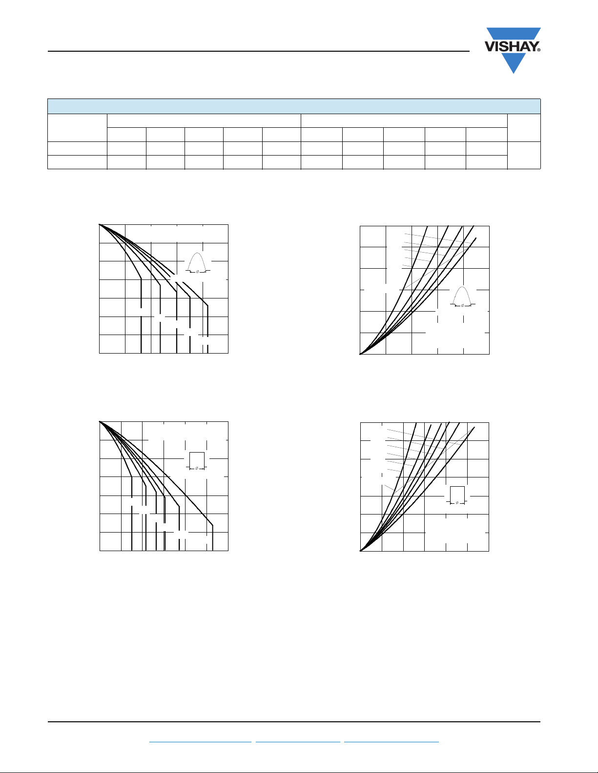
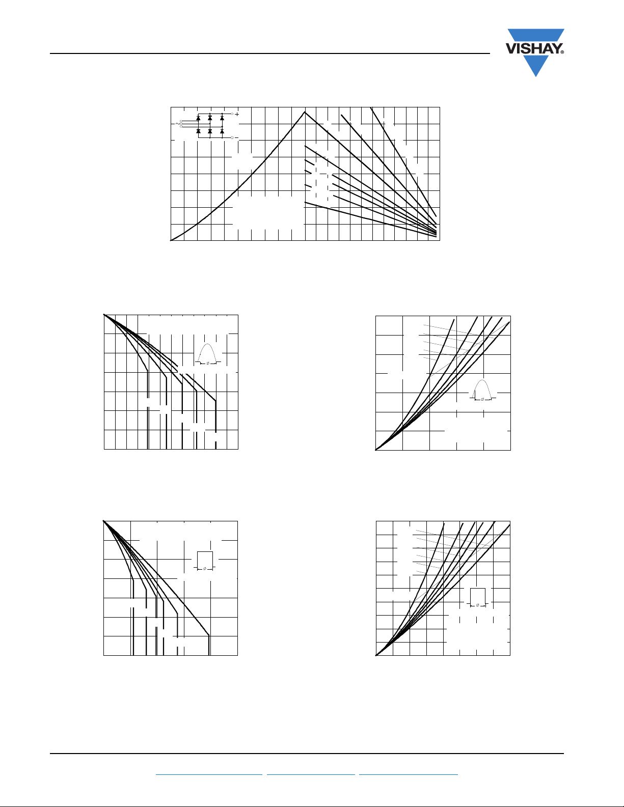
Fig. 1 - Current Ratings Characteristics
MAXIMUM RECTANGULAR CONDUCTION AT TJ MAXIMUM
J
when devices operate at different conduction angles than DC
thJC
)
300
250
200
150
100
50
0
Maximum Average On-state Power Loss (W
040801201602
180°
120°
90°
60°
30°
RMS Limit
VSK.170.. Series
Per Junction
T
J
Average On-state Current (A)
Conduction Angle
= 125°C
Fig. 3 - On-State Power Loss Characteristics
UNITS
K/W
00
Fig. 2 - Current Ratings Characteristics
www.vishay.com For technical questions within your region, please contact one of the following: Document Number: 94417
4 DiodesAmericas@vishay.com
Fig. 4 - On-State Power Loss Characteristics
, DiodesAsia@vishay.com, DiodesEurope@vishay.com Revision: 02-Jul-10

2000
2500
3000
3500
4000
4500
5000
110100
Number Of Equal Amplitude Half Cycle Current Pulses (N)
At Any Rated Load Condition And With
Rated V
RRM
Applied Following Surge.
Peak Half Sine W ave On-state Current (A)
VSK.170.. Series
Per Junction
Initial TJ = 130°C
@ 60 Hz 0.0083 s
@ 50 Hz 0.0100 s
2000
2500
3000
3500
4000
4500
5000
0.01 0.1 1
Peak Half Sine Wave On-state Current (A)
Pulse Train Duration (s)
Maximum Non Repetitive Surge Current
Versus Pul se Tra in Dur ation. Control
Of Conduction May Not Be Maintained .
Initial TJ = 130°C
No Voltage Reapplied
Rated V
RRM
Reapplied
VSK.170.. Series
Per Junction
VSK.170PbF, VSK.250PbF Series
SCR/SCR and SCR/Diode
Vishay Semiconductors
(MAGN-A-PAK Power Modules), 170 A/250 A
Fig. 5 - Maximum Non-Repetitive Surge Current Fig. 6 - Maximum Non-Repetitive Surge Current
400
350
300
180°
120°
90°
60°
30°
250
200
Conduction Angle
150
100
50
Maximum Total On-state Power Loss (W)
0
0 50 100 150 200 250 300 350 400
VSK.170.. Series
Per Module
T
J
Total RMS Output Current (A)
Fig. 7 - On-State Power Loss Characteristics
= 130°C
0
0
.
020406080100120
Maximum Allowable Ambient Temperature (°C)
0
0
0
.
2
5
K
/
.
3
K
/
W
3
5
K
/W
0.
.
1
.
2
W
1
6
2
K
K
/
/
W
W
R
0
.
0
t
8K
h
K
S
A
/
/
W
W
=
0
.
0
4
K
/
W
D
e
l
t
a
R
1000
900
800
700
600
500
400
300
200
Maximum Total Power Loss (W)
100
Document Number: 94417 For technical questions within your region, please contact one of the following: www.vishay.com
Revision: 02-Jul-10 DiodesAmericas@vishay.com
0
180°
(Sine)
180°
(Rect)
2 x VSK.170.. Series
Single Phase Bridge
Connected
= 130°C
T
J
0 50 100 150 200 250 300 350
Total Output Current (A)
Fig. 8 - On-State Power Loss Characteristics
, DiodesAsia@vishay.com, DiodesEurope@vishay.com 5
R
0
.
0
t
4
0
0
.
0
.
0
6
8
0
.
1
0
.1
2
0
.
1
6
K
0
.
2
K
/
0
.
2
5
K
0
.
3
5
K
K
K
/
W
K
/
W
K
/
W
/
W
W
/
W
/
W
h
S
K
A
/
W
/
W
=
0
.
0
2
K
/
W
D
e
l
t
a
R
0 20406080100120
Maximum Allowable Ambient Temperature (°C)
VSK.170PbF, VSK.250PbF Series
0 20406080100120
Maximum Allowable Ambient Temperature (°C)
0
.
2
5
K
/
W
0
.
1
6
K
/
W
0
.
1
2
K
/
W
0
.
1
K
/
W
0
.
0
8
K
/
W
0
.
0
5
K
/
W
0
.
0
3
K
/
W
R
=
0
.
0
1
K
/
W
D
e
l
t
a
R
t
h
S
A
0
200
400
600
800
1000
1200
1400
1600
0 100200300400500
Total Output Current (A)
Maximum Total Power Loss (W)
120°
(Rect)
3 x VSK.170.. Series
Three Phase Bridge
Connected
T
J
= 130°C
60
70
80
90
100
110
120
130
01002003004005
00
DC
30°
60°
90°
120°
180°
Average On-state Current (A)
Maximum Allowable Case Temperature (°C)
Conduction Per iod
VSK.250.. Series
R
thJC
(DC) = 0.125 K/W
0
50
100
150
200
250
300
350
400
450
500
0 50 100 150 200 250 300 350 4
00
DC
180°
120°
90°
60°
30°
RMS Limit
Conduction Period
Maximum Average On-state Power Loss (W)
Average On-state Current (A)
VSK.250.. Ser ies
Per Junction
T
J
= 130°C
Vishay Semiconductors
130
120
110
100
90
80
70
60
Maximum Allowable Case Temperature (°C)
0 50 100 150 200 250 3
Fig. 10 - Current Ratings Characteristics
VSK.250.. Series
(DC) = 0.125 K/W
R
thJC
Conduction Ang le
30°
60°
90°
120°
Average On-state Current (A)
SCR/SCR and SCR/Diode
(MAGN-A-PAK Power Modules), 170 A/250 A
Fig. 9 - On-State Power Loss Characteristics
)
180°
350
300
250
200
150
100
50
0
00
Maximum Average On-state Power Loss (W
050100150200250
Fig. 12 - On-State Power Loss Characteristics
180°
120°
90°
60°
30°
RMS Limit
Average On-state Current (A)
Conduction Angl e
VSK.250.. Series
Per Junction
T = 130°C
J
www.vishay.com For technical questions within your region, please contact one of the following: Document Number: 94417
6 DiodesAmericas@vishay.com
Fig. 11 - Current Ratings Characteristics
, DiodesAsia@vishay.com, DiodesEurope@vishay.com Revision: 02-Jul-10
Fig. 13 - On-State Power Loss Characteristics

3500
4000
4500
5000
5500
6000
6500
7000
7500
11010
0
Number Of Equal Ampli tu de Half Cycl e Curr ent Pulse s (N)
Peak Half Sine Wave On-state Current (A)
VSK.250.. Series
Per Junction
At Any Rate d Load Condition And With
Rated V
RRM
Applied Following Surge.
Initial T = 130°C
@ 60 Hz 0.0083 s
@ 50 Hz 0.0100 s
J
020406080100120
Maximum Allowable Ambient Temperature (°C)
0
.
3
K
/
W
0
.
2
5
K
/
W
0
.
2
0
K
/
W
0
.
1
6
K
/
W
0
.
1
2
K
/
W
0
.
0
8
K
/
W
0
.
0
5
K
/
W
R
=
0
.
0
2
K
/
W
D
e
l
t
a
R
t
h
S
A
0
100
200
300
400
500
600
700
0 100 200 300 400 500 6 00
180°
120°
90°
60°
30°
Maximum Total On-state Pow er Loss (W)
Conduction angle
Total RMS Output Current (A)
VSK.250.. Series
Per Module
T
J
= 130°C
VSK.170PbF, VSK.250PbF Series
SCR/SCR and SCR/Diode
Vishay Semiconductors
(MAGN-A-PAK Power Modules), 170 A/250 A
9000
8000
7000
6000
5000
4000
Peak Half Sine Wave On-state Current (A)
3000
Fig. 14 - Maximum Non-Repetitive Surge Current Fig. 15 - Maximum Non-Repetitive Surge Current
Maximum Non Repetitive Surge Current
Versus Pulse Train Duration. Control
Of Conduction May Not Be Maintained .
Initial TJ = 130°C
No Voltage Reapplied
Rated V
RRM
Reapplied
VSK.250.. Series
Per Junctio n
0.01 0.1 1
Pulse Train Duration (s)
1400
1200
1000
800
600
400
200
Document Number: 94417 For technical questions within your region, please contact one of the following: www.vishay.com
Revision: 02-Jul-10 DiodesAmericas@vishay.com
Maximum Total Power Loss (W)
Fig. 16 - On-State Power Loss Characteristics
180°
(Sine)
180°
(Rect)
2 x VSK.250.. Series
Single Phase Bridge
0
0
100 200 300 400 500
Total Output Current (A)
Fig. 17 - On-State Power Loss Characteristics
0.02
R
0
.
0
0
t
h
3
S
K
K
A
/
/
W
=
W
0
.
0
1
K
/
W
D
e
l
t
a
R
Connect ed
= 130°C
T
J
.
0
4
0
K
.
/
0
W
5
K
/
W
0
.
0
6
K
/
W
0
.
1
K
/
W
0
.
1
2
K
/
W
0
.
1
6
K
/
W
0
.
3
K
/
W
0 20406080100120
Maximum Allowable Ambient Temperature (°C)
, DiodesAsia@vishay.com, DiodesEurope@vishay.com 7

VSK.170PbF, VSK.250PbF Series
0 20406080100120
Maximum Allowable Am bient T emperature (°C)
R
=
0
.
0
1
K
/
W
D
e
l
t
a
R
0
.
0
3
K
/
W
0
.
0
4
K
/
W
0
.
0
5
K
/
W
0
.
0
6
K
/
W
0
.
0
8
K
/
W
0
.
1
K
/
W
0
.
1
2
K
/
W
0
.
1
6
K
/
W
0
.
2
0
K
/
W
0
.
2
5
K
/
W
t
h
S
A
0
200
400
600
800
1000
1200
1400
1600
1800
2000
0
100 200 300 400 500 600 700
Maximum Total Power Loss (W)
Total Output Current (A)
120°
(Rect)
3 x VSK.250.. Series
Three Phase Bridge
Connect ed
T
J
= 130°C
0.511.522.533.544.55
100
1000
10000
Instantaneous Forward Current (V)
Instantaneous Forward Voltage (V)
Tj = 25°C
Tj = 130°C
VSK.170 Series
Per Junction
0.5 1 1.5 2 2.5 3 3.5 4 4.5 5 5.5 6
100
1000
10000
Instantaneous Forward Current (V)
Instantaneous Forward Voltage (V)
Tj = 25°C
Tj = 130°C
VSK.250 Series
Per Junction
Vishay Semiconductors
Fig. 19 - On-State Voltage Drop Characteristics
SCR/SCR and SCR/Diode
(MAGN-A-PAK Power Modules), 170 A/250 A
Fig. 18 - On-State Power Loss Characteristics
1800
VSK.170.. Series
= 130 °C
T
1600
J
Per Junction
1400
1200
1000
800
600
400
200
Typical Reverse Recovery Charge - Qrr (µC)
0 102030405060708090100
Rate Of Fall Of On-state Current - di/dt (A/µs)
Fig. 21 - Reverse Recovery Charge Characteristics
ITM = 800 A
500 A
300 A
200 A
100 A
50 A
Fig. 20 - On-State Voltage Drop Characteristics
www.vishay.com For technical questions within your region, please contact one of the following: Document Number: 94417
8 DiodesAmericas@vishay.com
, DiodesAsia@vishay.com, DiodesEurope@vishay.com Revision: 02-Jul-10
2400
2200
2000
1800
1600
1400
1200
VSK.250.. Series
= 130 °C
T
T = 130 °C
J
J
Per Junction
Per Junction
ITM = 800 A
500 A
300 A
200 A
100 A
50 A
1000
800
600
400
200
Typical Reverse Recovery Charge - Qrr (µC)
0 1020304050607080901
00
Rate Of Fall Of On-state Current - di/dt (A/µs)
Fig. 22 - Reverse Recovery Charge Characteristics
0.1
1
10
100
0.001 0.01 0.1 1 10 1
00
VGD
IGD
(b)
(a)
Tj=2 5 °C
Tj=12 5 °C
Tj=-40 °C
(2) (3)
Instantaneous Gate Current (A)
Instantaneous Gate Voltage (V)
a) Recommended load line for
b) Recommended load line for
rated di/dt : 20 V, 10 ohms; tr < =1µs
tr<=1 µs
Rectangular gate pulse
<=30% rated di/dt : 10V, 20ohms
(1) PGM = 10W, tp = 4ms
(2) PGM = 20W, tp = 2ms
(3) PGM = 40W, tp = 1ms
(4) PGM = 60W, tp = 0.66ms
VSK.170/250 Series Frequency Limited by PG(AV)
(1) (4)
1
- Module type
2 - Circuit configuration (see dimensions - link at the end of datasheet)
3
- Current rating
4 - Voltage code x 100 = V
RRM
(see Voltage Ratings table)
Device code
51324
VSK T 250 - 20 PbF
5 - None = Standard production
PbF = Lead (Pb)-free
VSK.170PbF, VSK.250PbF Series
SCR/SCR and SCR/Diode
(MAGN-A-PAK Power Modules), 170 A/250 A
Fig. 23 - Gate Characteristics
1
Steady State Value:
thJC
0.1
R = 0.17 K/W
thJC
R = 0.125 K/W
thJC
(DC Operation)
VSK.170.. Series
VSK.250.. Series
Vishay Semiconductors
0.01
Transient Thermal Impedance Z (K/W)
0.001
0.001 0.01 0.1 1 10 100
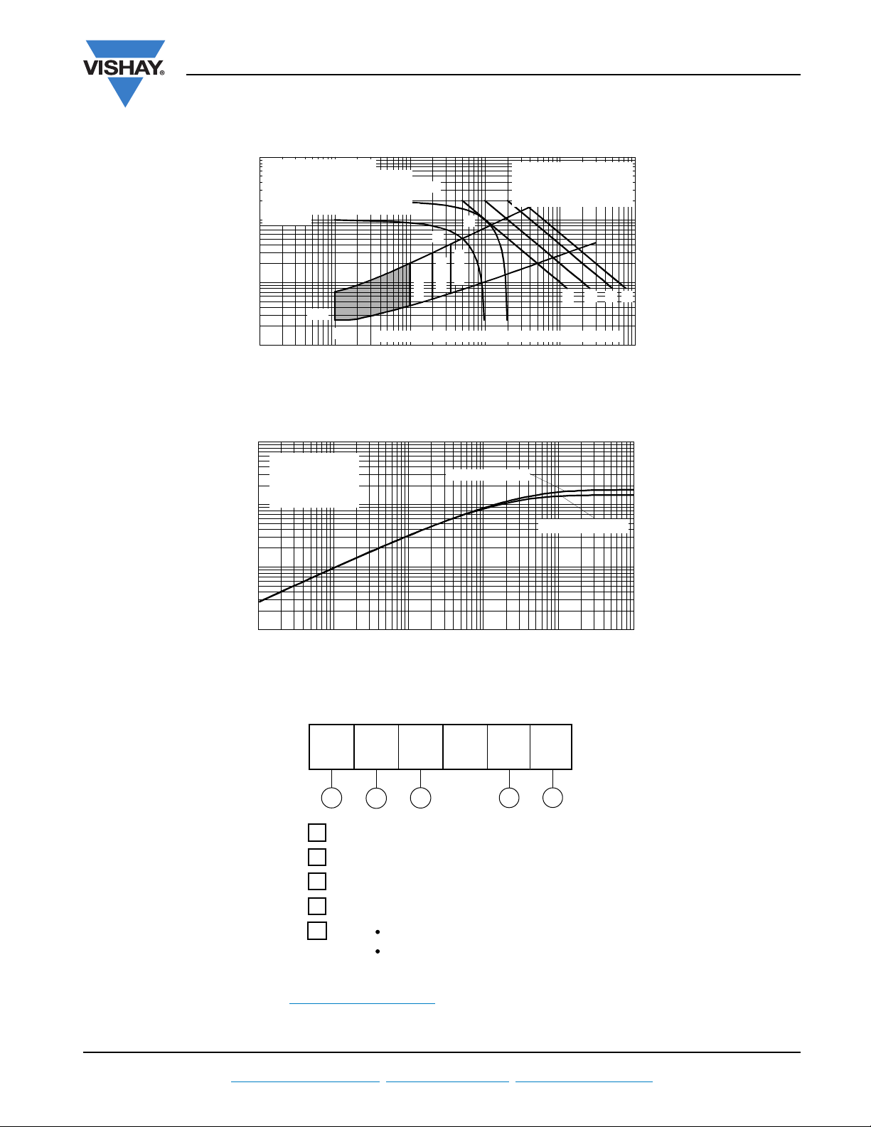
Fig. 24 - Thermal Impedance Z
ORDERING INFORMATION TABLE
Note
• To order the optional hardware go to www.vishay.com/doc?95172
Document Number: 94417 For technical questions within your region, please contact one of the following: www.vishay.com
Revision: 02-Jul-10 DiodesAmericas@vishay.com
Square Wave Pulse Duration (s)
Characteristics
thJC
, DiodesAsia@vishay.com, DiodesEurope@vishay.com 9

VSK.170PbF, VSK.250PbF Series
VSKL...
VSKU...
VSKV...
VSKH...
VSKT...
Available from 400 V to 1600 V for VSK.170PbF Series,
available from 400 V to 2000 V for VSK.250PbF Series
Available up to 1200 V,
contact factory for different requirement
+
-
~
~
+
-
K1
G1
G2
K2
+
-
~
~
+
-
K1
G1
+
-
~
~
+
-
-
-
+
+
-
-
K1
G1
G2
K2
+
+
-
-
+
+
K1
G1
G2
K2
Vishay Semiconductors
CIRCUIT CONFIGURATION
SCR/SCR and SCR/Diode
(MAGN-A-PAK Power Modules), 170 A/250 A
LINKS TO RELATED DOCUMENTS
Dimensions www.vishay.com/doc?95086
www.vishay.com For technical questions within your region, please contact one of the following: Document Number: 94417
10 DiodesAmericas@vishay.com
, DiodesAsia@vishay.com, DiodesEurope@vishay.com Revision: 02-Jul-10

DIMENSIONS in millimeters (inches)
Outline Dimensions
Vishay Semiconductors
MAGN-A-PAK
3 screws M8 x 1.25
20 (0.79)
32
(1.26)
HEX 13
9 (0.35)
35 (1.38) 28 (1.12)
80 (3.15)
115 (4.53)
Ø 5.5
6
38 (1.5)
6 (0.24)
51 (2.01)
(0.24)
50 (1.97)
52 (2.04)
10 (0.39)
Notes
• Dimensions are nominal
• Full engineering drawings are available on request
• UL identification number for gate and cathode wire: UL 1385
• UL identification number for package: UL 94 V-0
Document Number: 95086 For technical questions, contact: indmodules@vishay.com
Revision: 03-Aug-07 1
92 (3.62)
www.vishay.com

Legal Disclaimer Notice
Vishay
Disclaimer
ALL PRODUCT, PRODUCT SPECIFICATIONS AND DATA ARE SUBJECT TO CHANGE WITHOUT NOTICE TO IMPROVE
RELIABILITY, FUNCTION OR DESIGN OR OTHERWISE.
Vishay Intertechnology, Inc., its affiliates, agents, and employees, and all persons acting on its or their behalf (collectively,
“Vishay”), disclaim any and all liability for any errors, inaccuracies or incompleteness contained in any datasheet or in any other
disclosure relating to any product.
Vishay makes no warranty, representation or guarantee regarding the suitability of the products for any particular purpose or
the continuing production of any product. To the maximum extent permitted by applicable law, Vishay disclaims (i) any and all
liability arising out of the application or use of any product, (ii) any and all liability, including without limitation special,
consequential or incidental damages, and (iii) any and all implied warranties, including warranties of fitness for particular
purpose, non-infringement and merchantability.
Statements regarding the suitability of products for certain types of applications are based on Vishay’s knowledge of typical
requirements that are often placed on Vishay products in generic applications. Such statements are not binding statements
about the suitability of products for a particular application. It is the customer’s responsibility to validate that a particular
product with the properties described in the product specification is suitable for use in a particular application. Parameters
provided in datasheets and/or specifications may vary in different applications and performance may vary over time. All
operating parameters, including typical parameters, must be validated for each customer application by the customer’s
technical experts. Product specifications do not expand or otherwise modify Vishay’s terms and conditions of purchase,
including but not limited to the warranty expressed therein.
Except as expressly indicated in writing, Vishay products are not designed for use in medical, life-saving, or life-sustaining
applications or for any other application in which the failure of the Vishay product could result in personal injury or death.
Customers using or selling Vishay products not expressly indicated for use in such applications do so at their own risk and agree
to fully indemnify and hold Vishay and its distributors harmless from and against any and all claims, liabilities, expenses and
damages arising or resulting in connection with such use or sale, including attorneys fees, even if such claim alleges that Vishay
or its distributor was negligent regarding the design or manufacture of the part. Please contact authorized Vishay personnel to
obtain written terms and conditions regarding products designed for such applications.
No license, express or implied, by estoppel or otherwise, to any intellectual property rights is granted by this document or by
any conduct of Vishay. Product names and markings noted herein may be trademarks of their respective owners.
Document Number: 91000 www.vishay.com
Revision: 11-Mar-11 1
 Loading...