

Page 1
Preliminary
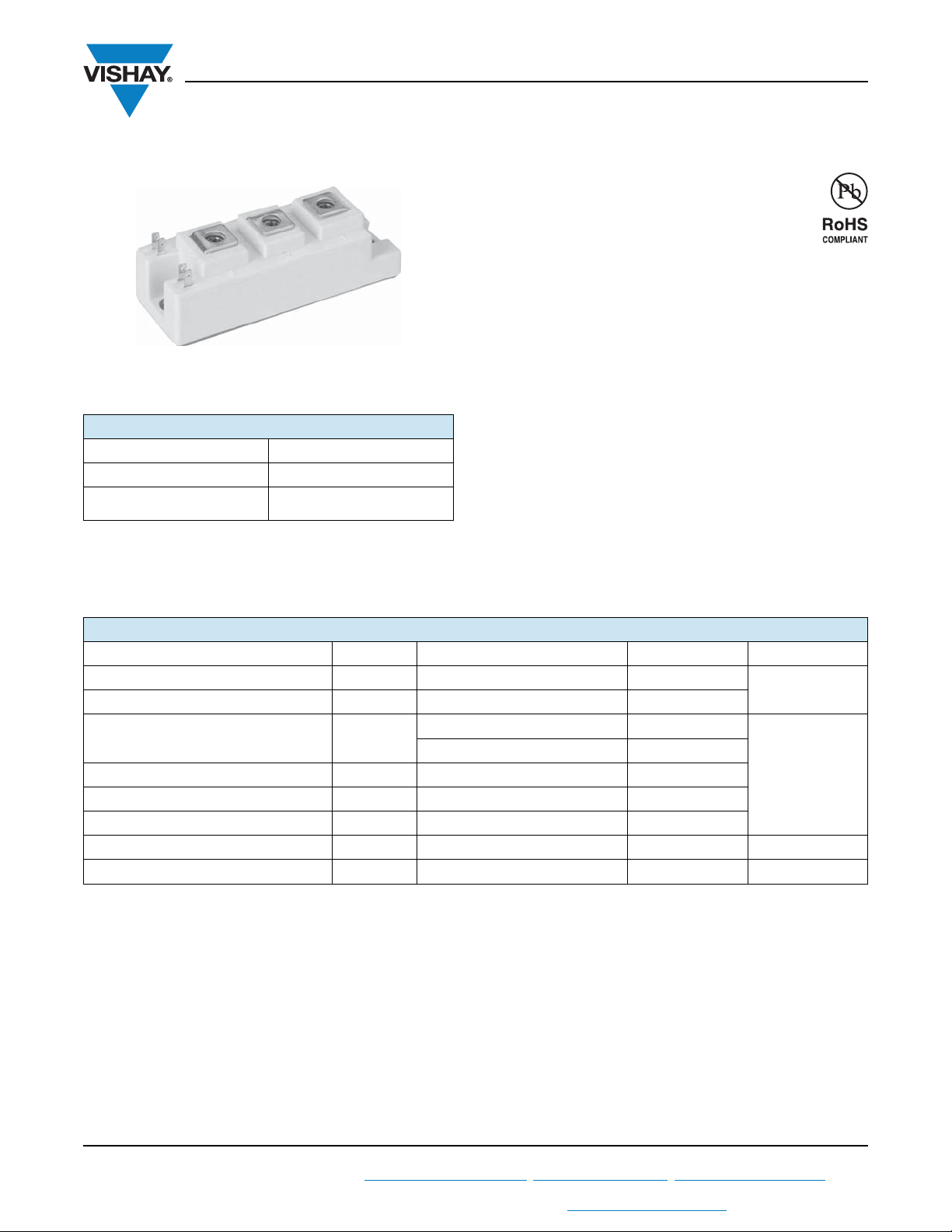
New INT-A-PAK
VS-GT100TP060N
www.vishay.com
Vishay Semiconductors
Half Bridge IGBT Power Module, 600 V, 100 A
FEATURES
•Low V
• 5 μs short circuit capability
•V
CE(sat)
• Maximum junction temperature 175 °C
• Low inductance case
• Fast and soft reverse recovery antiparallel FWD
• Isolated copper baseplate using DCB (Direct Copper
Bonding) technology
• Compliant to RoHS Directive 2002/95/EC
trench IGBT technology
CE(sat)
with positive temperature coefficient
PRODUCT SUMMARY
V
CES
at TC = 80 °C 100 A
I
C
(typical)
V
CE(on)
at I
= 100 A, 25 °C
C
600 V
1.65 V
TYPICAL APPLICATIONS
• UPS (Uninterruptable Power Supply)
• Switching mode power supplies
• Electronic welders
DESCRIPTION
Vishay’s IGBT power module provides ultra low conduction
loss as well as short circuit ruggedness. It is designed for
applications such as UPS and SMPS.
ABSOLUTE MAXIMUM RATINGS (TC = 25 °C unless otherwise noted)
PARAMETER SYMBOL TEST CONDITIONS MAX. UNITS
Collector to emitter voltage V
Gate to emitter voltage V
Collector current I
Pulsed collector current I
Diode continuous forward current I
Diode maximum forward current I
Maximum power dissipation P
RMS isolation voltage V
Note
(1)
Repetitive rating: Pulse width limited by maximum junction temperature.
CM
FM
CES
GES
C
F
ISOL
TC = 25 °C 160
T
= 80 °C 100
C
(1)
(1)
D
tp = 1 ms 200
TC = 80 °C 100
tp = 1 ms 200
TJ = 175 °C 417 W
f = 50 Hz, t = 1 min 4000 V
600
± 20
V
A
Revision: 13-Dec-11
For technical questions within your region: DiodesAmericas@vishay.com
THIS DOCUMENT IS SUBJECT TO CHANGE WITHOUT NOTICE. THE PRODUCTS DESCRIBED HEREIN AND THIS DOCUMENT
ARE SUBJECT TO SPECIFIC DISCLAIMERS, SET FORTH AT www.vishay.com/doc?91000
1
, DiodesAsia@vishay.com, DiodesEurope@vishay.com
Document Number: 93799
Page 2
Preliminary
VS-GT100TP060N
www.vishay.com
IGBT ELECTRICAL SPECIFICATIONS (TC = 25 °C unless otherwise noted)
PARAMETER SYMBOL TEST CONDITIONS MIN. TYP. MAX. UNITS
Collector to emitter breakdown voltage V
(BR)CES
TJ = 25 °C 600 - -
VGE = 15 V, IC = 100 A, TJ = 25 °C - 1.65 2.10
Gate to emitter threshold voltage V
Collector cut-off current I
Gate to emitter leakage current I
CE(sat)
GE(th)
CES
GES
V
= 15 V, IC = 100 A, TJ = 175 °C - 2.00 -
GE
VCE = VGE, IC = 1.0 mA, TJ = 25 °C 4.0 4.4 6.5
VCE = V
VGE = V
, VGE = 0 V, TJ = 25 °C - - 5.0 mA
CES
, VCE = 0 V, TJ = 25 °C - - 400 nA
GES
SWITCHING CHARACTERISTICS
PARAMETER SYMBOL TEST CONDITIONS MIN. TYP. MAX. UNITS
Turn-on delay time t
Rise time t
Turn-off delay time t
Fall time t
Turn-on switching loss E
Turn-off switching loss E
Turn-on delay time t
Rise time t
Turn-off delay time t
Fall time t
Turn-on switching loss E
Turn-off switching loss E
Input capacitance C
Reverse transfer capacitance C
SC data I
Stray inductance L
Module lead resistance, terminal to chip R
d(on)
r
d(off)
f
on
off
d(on)
r
d(off)
f
on
off
ies
oes
res
SC
CE
CC’+EE’
VCC = 300 V, IC = 100 A, Rg = 2.2 ,
V
= ± 15 V, TJ = 25 °C
GE
VCC = 300 V, IC = 100 A, Rg = 2.2 ,
V
= ± 15 V, TJ = 125 °C
GE
VGE = 0 V, VCE = 30 V, f = 1.0 MHz
tp 5 μs, VGE = 15 V, TJ = 125 °C,
V
= 360 V, V
CC
CEM
1200 V
Vishay Semiconductors
VCollector to emitter saturation voltage V
- 106 -
-49-
- 102 -
-85-
-0.46-
-0.95-
- 112 -
-62-
- 126 -
- 109 -
-0.78-
-1.73-
-7.71-
-0.53-
-0.23-
- 900 - A
- - 30 nH
-0.75- m
ns
mJ
ns
mJ
nFOutput capacitance C
DIODE ELECTRICAL SPECIFICATIONS (TC = 25 °C unless otherwise noted)
PARAMETER SYMBOL TEST CONDITIONS MIN. TYP. MAX. UNITS
= 25 °C - 1.40 1.80
T
Forward voltage V
Reverse recovery charge Q
F
rr
IF = 100 A
IF = 100 A, VR = 600 V,
R
Peak reverse recovery current I
Reverse recovery energy E
rr
rec
Revision: 13-Dec-11
For technical questions within your region: DiodesAmericas@vishay.com
= 5.6
G
V
GE
2
= - 15 V
, DiodesAsia@vishay.com, DiodesEurope@vishay.com
THIS DOCUMENT IS SUBJECT TO CHANGE WITHOUT NOTICE. THE PRODUCTS DESCRIBED HEREIN AND THIS DOCUMENT
ARE SUBJECT TO SPECIFIC DISCLAIMERS, SET FORTH AT www.vishay.com/doc?91000
J
T
= 125 °C - 1.40 -
J
= 25 °C - 5.5 -
T
J
T
= 125 °C - 7.3 -
J
TJ = 25 °C - 68 -
T
= 125 °C - 88 -
J
TJ = 25 °C - 0.89 -
T
= 125 °C - 1.71 -
J
Document Number: 93799
V
μC
A
mJ
Page 3

Preliminary
I
C
(A)
VCE (V)
0
25
50
75
100
125
150
175
200
0 0.5 1 1.5 2 2.5 3 3.5
175 °C
25 °C
VGE = 15 V
0
25
50
75
100
125
150
175
200
45678910
25 °C
175 °C
VCE = 50 V
VGE (V)
I
C
(A)
E (mJ)
Rg (Ω)
E
on
E
off
0
1
2
3
4
5
6
7
0 1020304050
V
CC = 300 V
I
C
= 100 A
V
GE
= ± 15 V
T
J
= 125 °C
VS-GT100TP060N
www.vishay.com
THERMAL AND MECHANICAL SPECIFICATIONS
PARAMETER SYMBOL TEST CONDITIONS MIN. TYP. MAX. UNITS
Maximum junction temperature T
Storage temperature range T
Junction to case
IGBT
Case to sink (Conductive grease applied) R
Mounting torque
Weight - 150 - g
R
J
Stg
thJC
thCS
Power terminal screw: M5 2.5 to 5.0
Mounting screw: M6 3.0 to 5.0
5
V
CC = 300 V
4.5
R
= 2.2 Ω
G
4
V
GE
= 125 °C
T
3.5
J
3
2.5
E (mJ)
2
1.5
1
0.5
0
0 50 100 150 200
Vishay Semiconductors
- - 175
- 40 - 125
- - 0.36
-0.05-
= ± 15 V
E
ON
E
OFF
IC (A)
°C
K/WDiode - - 0.57
Nm
Fig. 1 - IGBT Typical Output Characteristics
Revision: 13-Dec-11
Fig. 2 - IGBT Transfer Characteristics
For technical questions within your region: DiodesAmericas@vishay.com
THIS DOCUMENT IS SUBJECT TO CHANGE WITHOUT NOTICE. THE PRODUCTS DESCRIBED HEREIN AND THIS DOCUMENT
ARE SUBJECT TO SPECIFIC DISCLAIMERS, SET FORTH AT www.vishay.com/doc?91000
Fig. 3 - IGBT Switching Loss vs. I
Fig. 4 - IGBT Switching Loss vs. R
3
Document Number: 93799
C
G
, DiodesAsia@vishay.com, DiodesEurope@vishay.com
Page 4

www.vishay.com
0.01
0.1
1
0.001 0.01 0.1 1 10
t (s)
Z
thJC
(K/W)
IGBT
(A)
C
I
Preliminary
250
200
150
100
RG = 2.2 Ω
= ± 15 V
V
50
GE
= 125 °C
T
J
0
0100 300200 400 500 700600
VCE (V)
Fig. 5 - RBSOA
Module
VS-GT100TP060N
Vishay Semiconductors
Fig. 6 - IGBT Transient Thermal Impedance
200
175
150
125
100
(A)
F
I
75
50
25
0
0 0.5 1 1.5 2
125 °C
25 °C
2.5
1.5
E (mJ)
0.5
VF (V)
Fig. 7 - Diode Forward Characteristics Fig. 8 - Diode Switching Loss vs. I
Revision: 13-Dec-11
For technical questions within your region: DiodesAmericas@vishay.com
THIS DOCUMENT IS SUBJECT TO CHANGE WITHOUT NOTICE. THE PRODUCTS DESCRIBED HEREIN AND THIS DOCUMENT
ARE SUBJECT TO SPECIFIC DISCLAIMERS, SET FORTH AT www.vishay.com/doc?91000
4
, DiodesAsia@vishay.com, DiodesEurope@vishay.com
V
CC = 300 V
= 2.2 Ω
R
G
2
1
0
= - 15 V
V
GE
= 125 °C
T
J
E
REC
0 50 100 150 200
IF (A)
Document Number: 93799
F
Page 5

www.vishay.com
0
0.2
0.4
0.6
0.8
1
1.2
1.4
1.6
1.8
2
0 1020304050
E (mJ)
R
G
(Ω)
E
REC
VCC = 300 V
I
F
= 100 A
V
GE
= - 15 V
T
J
= 125 °C
1
6
7
3
2
5
4
Preliminary
VS-GT100TP060N
Vishay Semiconductors
1
(K/W)
0.1
thJC
Z
0.01
0.001 0.01 0.1 1 10
CIRCUIT CONFIGURATION
Fig. 9 - Diode Switching Loss vs. R
Diode
G
t (s)
Fig. 10 - Forward Characteristics of Diode
Revision: 13-Dec-11
For technical questions within your region: DiodesAmericas@vishay.com
THIS DOCUMENT IS SUBJECT TO CHANGE WITHOUT NOTICE. THE PRODUCTS DESCRIBED HEREIN AND THIS DOCUMENT
ARE SUBJECT TO SPECIFIC DISCLAIMERS, SET FORTH AT www.vishay.com/doc?91000
5
Document Number: 93799
, DiodesAsia@vishay.com, DiodesEurope@vishay.com
Page 6

www.vishay.com
DIMENSIONS in millimeters
40
4.5
17
23 23
Preliminary
VS-GT100TP060N
Vishay Semiconductors
3 - M5.0
12.5
754
6
4.5 17
18.97 18.98
6.92
23.5
13.64 13 13.64
80
94.1
123
34
2 - Ø 6.4
22.2
30.58
7.2
31.4
Revision: 13-Dec-11
For technical questions within your region: DiodesAmericas@vishay.com
6
, DiodesAsia@vishay.com, DiodesEurope@vishay.com
Document Number: 93799
THIS DOCUMENT IS SUBJECT TO CHANGE WITHOUT NOTICE. THE PRODUCTS DESCRIBED HEREIN AND THIS DOCUMENT
ARE SUBJECT TO SPECIFIC DISCLAIMERS, SET FORTH AT www.vishay.com/doc?91000
 Loading...