Vishay VS-GB100TS60NPbF Data Sheet

www.vishay.com
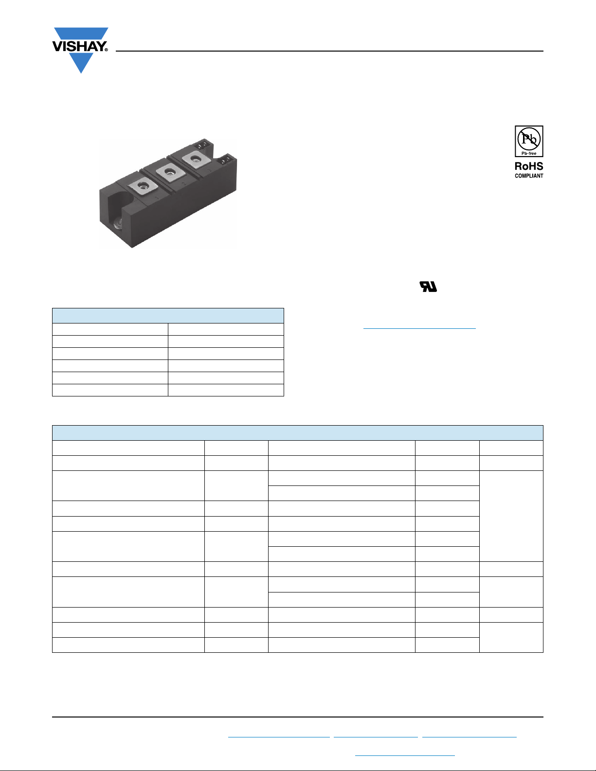
INT-A-PAK
PRODUCT SUMMARY
V
CES
I
DC 108 A
C
V
at 100 A, 25 °C 2.6 V
CE(on)
Speed 8 kHz to 30 kHz
Package INT-A-PAK
Circuit Half bridge
VS-GB100TS60NPbF
INT-A-PAK “Half-Bridge”
(Ultrafast Speed IGBT), 108 A
FEATURES
• Generation 5 Non Punch Through (NPT)
technology
• Ultrafast: optimized for hard switching speed
•Low V
• 10 μs short circuit capability
• Square RBSOA
•Positive V
•HEXFRED
• Industry standard package
•Al
• UL approved file E78996
• Designed for industrial level
• Material categorization: for definitions of compliance
600 V
BENEFITS
• Benchmark efficiency for UPS and welding application
• Rugged transient performance
• Direct mounting on heatsink
• Very low junction to case thermal resistance
CE(on)
temperature coefficient
CE(on)
®
antiparallel diode with ultrasoft reverse
recovery characteristics
DBC
2O3
please see www.vishay.com/doc?99912
Vishay Semiconductors
ABSOLUTE MAXIMUM RATINGS
PARAMETER SYMBOL TEST CONDITIONS MAX. UNITS
Collector to emitter voltage V
Continuous collector current I
Pulsed collector current I
Clamped inductive load current I
Diode continuous forward current I
Gate to emitter voltage V
Maximum power dissipation P
Isolation voltage V
Operating junction temperature range T
Storage temperature range T
Revision: 10-Jun-15
For technical questions within your region: DiodesAmericas@vishay.com
THIS DOCUMENT IS SUBJECT TO CHANGE WITHOUT NOTICE. THE PRODUCTS DESCRIBED HEREIN AND THIS DOCUMENT
ARE SUBJECT TO SPECIFIC DISCLAIMERS, SET FORTH AT www.vishay.com/doc?91000
CES
C
CM
LM
F
GE
D
ISOL
J
Stg
TC = 25 °C 108
= 80 °C 74
T
C
TC = 25 °C 106
= 80 °C 69
T
C
TC = 25 °C 390
T
= 80 °C 219
C
Any terminal to case, t = 1 min 2500 V
1
, DiodesAsia@vishay.com, DiodesEurope@vishay.com
600 V
200
200
± 20 V
-40 to +150
-40 to +150
Document Number: 94501
A
W
°C

VS-GB100TS60NPbF
www.vishay.com
ELECTRICAL SPECIFICATIONS (TJ = 25 °C unless otherwise specified)
PARAMETER SYMBOL TEST CONDITIONS MIN. TYP. MAX. UNITS
Collector to emitter breakdown voltage V
BR(CES)VGE
= 0 V, IC = 500 μA 600 - -
VGE = 15 V, IC = 50 A - 1.95 2.1
V
= 15 V, IC = 100 A - 2.6 2.85
GE
V
= 15 V, IC = 50 A, TJ = 125 °C - 2.21 2.44
GE
V
= 15 V, IC = 100 A, TJ = 125 °C - 3.05 3.38
GE
VCE = VGE, IC = 500 μA 3 4.6 6
VGE = 0 V, VCE = 600 V - 0.01 0.1
= 0 V, VCE = 600 V, TJ = 150 °C - 3.7 10
V
GE
Gate threshold voltage V
Collector to emitter leakage current I
CE(on)
GE(th)
CES
IC = 50 A - 1.35 1.66
I
= 100 A - 1.57 1.96
Diode forward voltage drop V
Gate to emitter leakage current I
FM
GES
C
I
= 50 A, TJ = 125 °C - 1.27 1.50
C
I
= 100 A, TJ = 125 °C - 1.57 1.89
C
VGE = ± 20 V - - ± 200 nA
SWITCHING CHARACTERISTICS (TJ = 25 °C unless otherwise specified)
PARAMETER SYMBOL TEST CONDITIONS MIN. TYP. MAX. UNITS
Turn-on switching loss E
Turn-off switching loss E
Total switching loss E
Turn-on switching loss E
Turn-off switching loss E
Total switching loss E
Turn-on delay time t
Rise time t
Turn-off delay time t
Fall time t
Reverse bias safe operating area RBSOA
Short circuit safe operating area SCSOA
Diode reverse recovery time t
Diode peak reverse current I
Diode recovery charge Q
Diode reverse recovery time t
Diode peak reverse current I
Diode recovery charge Q
on
off
tot
on
off
tot
d(on)
r
d(off)
f
rr
rr
rr
rr
IC = 100 A, VCC = 360 V, VGE = 15 V,
R
= 4.7 , L = 200 μH, TJ = 25 °C
g
IC = 100 A, VCC = 360 V, VGE = 15 V,
R
= 4.7 , L = 200 μH, TJ = 125 °C
g
T
= 150 °C, IC = 200 A,
J
R
= 27 VGE = 15 V to 0
g
T
= 150 °C, VCC = 400 V, VP = 600 V,
J
R
= 27 VGE = 15 V to 0
g
IF = 50 A, dIF/dt = 200 A/μs,
V
= 400 V, TJ = 25 °C
rr
CC
IF = 50 A, dIF/dt = 200 A/μs,
V
= 400 V, TJ = 125 °C
rr
CC
Vishay Semiconductors
VCollector to emitter voltage V
mA
V
-0.6-
-1.1-
-1.7-
-0.8-
-1.3-
-2.1-
- 197 -
-50-
- 225 -
-72-
Fullsquare
10 - -
- 116 140 ns
-1115A
- 600 1050 nC
- 152 190 ns
-1620A
- 1215 1900 nC
mJ
ns
THERMAL AND MECHANICAL SPECIFICATIONS
PARAMETER SYMBOL MIN. TYP. MAX. UNITS
Operating junction and storage temperature range T
Junction to case per leg
IGBT
Case to sink per module R
Mounting torque
case to heatsink - - 4
case to terminal 1, 2, 3 - - 3
Weight - 185 - g
Revision: 10-Jun-15
For technical questions within your region: DiodesAmericas@vishay.com
THIS DOCUMENT IS SUBJECT TO CHANGE WITHOUT NOTICE. THE PRODUCTS DESCRIBED HEREIN AND THIS DOCUMENT
ARE SUBJECT TO SPECIFIC DISCLAIMERS, SET FORTH AT www.vishay.com/doc?91000
J
R
, T
thJC
thCS
Stg
-40 - 150 °C
-0.230.32
-0.1-
2
Document Number: 94501
, DiodesAsia@vishay.com, DiodesEurope@vishay.com
°C/WDiode - 0.38 0.64
Nm

www.vishay.com
I
cE
(A)
VCE(V)
0123456
0
50
100
150
200
Vge = 9V
Vge = 18V
Vge = 15V
Vge = 12V
I
cE
(A)
VGE(V)
0246810
0
20
40
60
80
100
120
140
160
180
200
Tj = 25°C
Tj = 125°C
0 20406080100120140160
1.5
2
2.5
3
3.5
4
4.5
5
Ic = 50A
Ic = 100A
Ic = 200A
TJ, Junction Temperature (°C)
V
CE
, Collector -to-Emitter Voltage (V)
0 20 40 60 80 100 120
0
20
40
60
80
100
120
140
160
DC
T
C
, Case Temperature (°C)
Maximum DC Collector Current (A)
VS-GB100TS60NPbF
Vishay Semiconductors
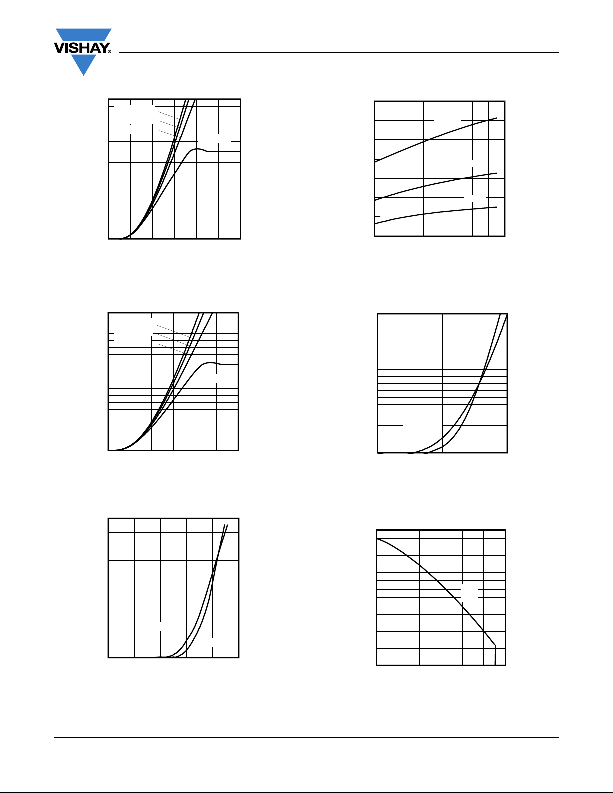
Fig. 1 - Typical IGBT Output Characteristics
T
= 25 °C, tp = 500 μs
J
200
Vge = 18V
Vge = 15V
Vge = 12V
150
(A)
100
cE
I
50
0
0123456
Vge = 9V
VCE(V)
Fig. 2 - Typical IGBT Output Characteristics
T
= 125 °C, tp = 500 μs
J
Fig. 4 - Typical Collector to Emitter Voltage vs.
Junction Temperature,
= 15 V, 500 μs pulse width
V
GE
200
150
100
(A)
F
I
50
Tj = 125°C
Tj = 25°C
0
0.0 0.5 1.0 1.5 2.0
VF(V)
Fig. 5 - Diode Forward Characteristics, t
= 500 μs
p
Revision: 10-Jun-15
Fig. 3 - Typical Transfer Characteristics
For technical questions within your region: DiodesAmericas@vishay.com
THIS DOCUMENT IS SUBJECT TO CHANGE WITHOUT NOTICE. THE PRODUCTS DESCRIBED HEREIN AND THIS DOCUMENT
V
= 20 V, tp = 500 μs
CE
Fig. 6 - Maximum Collector Current vs.
Case Temperature
3
, DiodesAsia@vishay.com, DiodesEurope@vishay.com
ARE SUBJECT TO SPECIFIC DISCLAIMERS, SET FORTH AT www.vishay.com/doc?91000
Document Number: 94501
 Loading...