

FlipKY
®
VS-FCSP07H40TR
www.vishay.com
Vishay Semiconductors
FlipKY®,
Chip Scale Package Schottky Barrier Rectifier, 0.75 A
FEATURES
•Ultra low VF to footprint area
• Very low profile (< 0.6 mm)
• Low thermal resistance
• Supplied tested and on tape and reel
• Compliant to RoHS Directive 2002/95/EC
APPLICATIONS
• Reverse polarity protection
• Current steering
• Freewheeling
• Flyback
•Oring
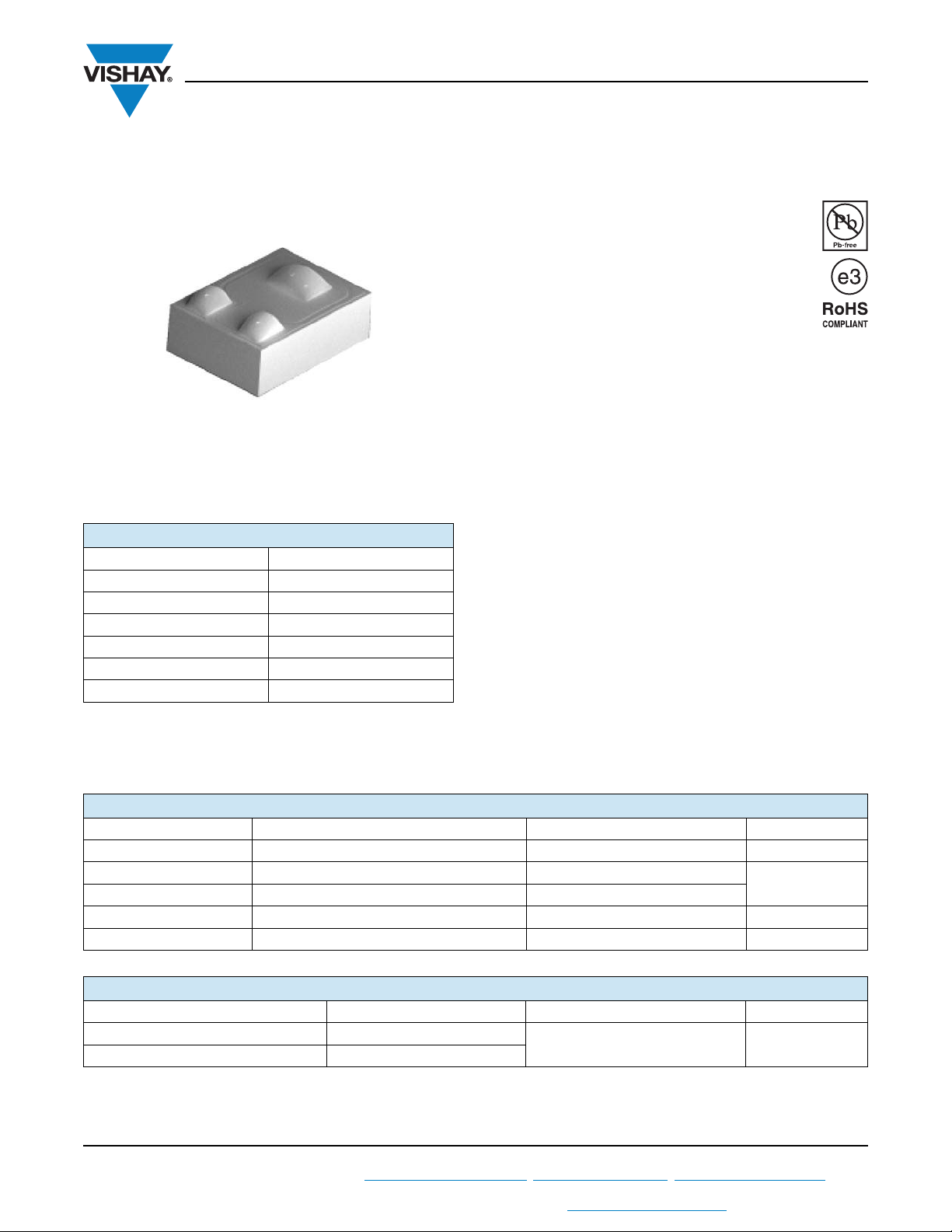
DESCRIPTION
PRODUCT SUMMARY
I
F(AV)
V
R
V
at I
F
F
I
max. at 25 °C 10 μA
RM
I
max. at 125 °C 3 mA
RM
max. 150 °C
T
J
E
AS
0.75 A
40 V
0.47 V
5 mJ
Vishay’s FlipKY® product family utilizes wafer level
chip scale packaging to deliver Schottky diodes with the
lowest V
to PCB footprint area in industry. The three pad
F
0.9 mm x 1.2 mm devices can deliver up to 0.75 A and
2
occupy only 1.08 mm
of board space. The anode and
cathode connections are made through solder bump pads
on one side of the silicon enabling designers to strategically
place the diodes on the PCB. This design not only minimizes
board space but also reduces thermal resistance and
inductance, which can improve overall circuit efficiency.
Typical applications include hand-held, portable equipment
such as cell phones, MP3 players, bluetooth, GPS, PDAs,
and portable hard disk drives where space savings and
performance are crucial.
MAJOR RATINGS AND CHARACTERISTICS
SYMBOL CHARACTERISTICS MAX. UNITS
V
I
F(AV)
I
FSM
V
T
RRM
F
J
Rectangular waveform 0.75
0.75 Apk, TJ = 125 °C 0.47 V
40 V
190
- 55 to 150 °C
A
VOLTAGE RATINGS
PARAMETER SYMBOL VS-FCSP07H40TR UNITS
Maximum DC reverse voltage V
Maximum working peak reverse voltage V
Revision: 04-Jul-11
For technical questions within your region: DiodesAmericas@vishay.com
THIS DOCUMENT IS SUBJECT TO CHANGE WITHOUT NOTICE. THE PRODUCTS DESCRIBED HEREIN AND THIS DOCUMENT
ARE SUBJECT TO SPECIFIC DISCLAIMERS, SET FORTH AT www.vishay.com/doc?91000
R
RWM
40 V
1
, DiodesAsia@vishay.com, DiodesEurope@vishay.com
Document Number: 94561
dP
tot
dT
J
-------------
1
R
thJA
--------------<
VS-FCSP07H40TR
www.vishay.com
ABSOLUTE MAXIMUM RATINGS
PARAMETER SYMBOL TEST CONDITIONS VALUES UNITS
Maximum average forward current I
Maximum peak one cycle
non-repetitive surge current at 25 °C
Non-repetitive avalanche energy E
Repetitive avalanche current I
F(AV)
I
FSM
AR
50 % duty cycle at T
5 µs sine or 3 µs rect. pulse
10 ms sine or 6 ms rect. pulse 10
AS
TJ = 25 °C, IAS = 2.0 A, L = 5.0 mH 5mJ
Current decaying linearly to zero in 1 μs
Frequency limited by T
= 106 °C, rectangular waveform 0.75
PCB
Following any rated
load condition and with
rated V
maximum VA = 1.5 x VR typical
J
ELECTRICAL SPECIFICATIONS
PARAMETER SYMBOL TEST CONDITIONS TYP. MAX. UNITS
0.75 A
Maximum forward voltage drop
See fig. 1
V
FM
1.5 A 0.59 0.64
(1)
0.75 A
1.5 A 0.52 0.57
TJ = 25 °C
Maximum reverse leakage current
See fig. 2
Maximum junction capacitance C
(1)
I
RM
T
J
VR = 5 VDC (test signal range 100 kHz to 1 MHz), 25 °C -90pF
T
Maximum voltage rate of charge dV/dt Rated V
Note
(1)
Pulse width < 300 μs, duty cycle < 2 %
= 125 °C
R
T
= 25 °C
J
= 125 °C
T
J
V
= Rated V
R
= 20 V 0.2 0.5
V
R
= 10 V 0.08 0.25
V
R
V
= 5 V 0.05 0.15
R
V
= Rated V
R
= 20 V 0.2 1
V
R
V
= 10 V 0.15 0.8
R
= 5 V 0.125 0.5
V
R
Vishay Semiconductors
190
applied
RRM
0.5 A
0.51 0.55
0.42 0.47
R
R
110
0.7 3
- 10 000 V/µs
A
V
µA
mA
THERMAL - MECHANICAL SPECIFICATIONS
PARAMETER SYMBOL TEST CONDITIONS VALUES UNITS
Maximum junction and
storage temperature range
Typical thermal resistance,
junction to PCB
Maximum thermal resistance,
junction to ambient
Notes
(1)
(2)
Mounted on minimum footprint PCB
thermal runaway condition for a diode on its own heatsink
Revision: 04-Jul-11
For technical questions within your region: DiodesAmericas@vishay.com
THIS DOCUMENT IS SUBJECT TO CHANGE WITHOUT NOTICE. THE PRODUCTS DESCRIBED HEREIN AND THIS DOCUMENT
ARE SUBJECT TO SPECIFIC DISCLAIMERS, SET FORTH AT www.vishay.com/doc?91000
(1)
T
, T
J
Stg
(2)
R
thJL
DC operation 35
- 55 to 150 °C
°C/W
R
thJA
2
150
Document Number: 94561
, DiodesAsia@vishay.com, DiodesEurope@vishay.com

Forward Voltage Drop - VFM (V)
Instantaneous Forward Current - I
F
(A)
0.1
1
10
0.2 0.4 0.6 0.8 1 1
.2
T = 150˚C
T = 125˚C
T = 25˚C
J
J
J
Reverse Voltage - VR (V)
Reverse Current - I
R
(μA)
0.01
0.1
1
10
100
1000
0000
0 5 10 15 20 25 30 35 4
125˚C
100˚C
75˚C
50˚C
25˚C
Tj = 150˚C
www.vishay.com
Fig. 1 - Maximum Forward Voltage Drop Characteristics
(Per Leg)
VS-FCSP07H40TR
Vishay Semiconductors
1000
T = 25˚C
J
(p F)
T
100
Junction Capacitance - C
10
0 5 10 15 20 25 30 35 40
Reverse Voltage - VR (V)
Fig. 3 - Typical Junction Capacitance vs.
Reverse Voltage (Per Leg)
160
160
150
150
140
140
130
130
120
120
110
110
100
100
90
90
Square wave (D=0.50)
Square wave (D=0.50)
80
80
80% rated Vr applied
Allowable Case Temperature (°C)
Allowable Case Temperature (°C)
80% rated Vr applied
70
70
see note (2)
see note (1)
60
60
0 0.2 0.4 0.6 0.8 1.00 0.2 0.4 0.6 0.8 1.0
0 0.2 0.4 0.6 0.8 1.00 0.2 0.4 0.6 0.8 1.0
Average Forward Current - I
Average Forward Current - I
Fig. 4 - Maximum Allowable Case Temperature vs.
Average Forward Current (Per Leg)
D = 0.75
D = 0.75
D = 0.50
D = 0.50
D = 0.33
D = 0.33
D = 0.25
D = 0.25
D = 0.20
D = 0.20
DC
DC
F(AV)
F(AV)
(A)
(A)
1.2
1.2
1
Note
(1)
Formula used: TC = TJ - (Pd + Pd
Pd = Forward power loss = I
Revision: 04-Jul-11
For technical questions within your region: DiodesAmericas@vishay.com
THIS DOCUMENT IS SUBJECT TO CHANGE WITHOUT NOTICE. THE PRODUCTS DESCRIBED HEREIN AND THIS DOCUMENT
Fig. 2 - Typical Values of Reverse Current vs.
Reverse Voltage (Per Leg)
ARE SUBJECT TO SPECIFIC DISCLAIMERS, SET FORTH AT www.vishay.com/doc?91000
REV
x VFM at (I
F(AV)
) x R
;
thJC
/D) (see fig. 6); Pd
F(AV)
0.6
D = 0.20
D = 0.25
0.5
D = 0.33
D = 0.50
0.4
0.3
D = 0.75
RMS Limit
DC
0.2
Average Power Loss (Watts)
0.1
0
0
0 0.2 0.4 0.6 0.8 1
Average Forward Current - I
F(AV)
1.2
(A)
Fig. 5 - Forward Power Loss Characteristics (Per Leg)
= Inverse power loss = VR1 x IR (1 - D); IR at 80 % VR applied
REV
3
Document Number: 94561
, DiodesAsia@vishay.com, DiodesEurope@vishay.com

www.vishay.com
Square Wave Pulse Duration - tp (microsec)
Non-Repetitive Surge Current - I
FSM
(A)
1
10
100
1
000
10 100 1000 10000
At Any Rated Load Condition
And With Rated Vrrm Applied
Following Surge
VS-FCSP07H40TR
Vishay Semiconductors
Fig. 6 - Maximum Non-Repetitive Surge Current (Per Leg)
L
High-speed
switch
Freewheel
diode
40HFL40S02
V
= 25 V
d
+
Current
monitor
D.U.T.
IRFP460
= 25 Ω
R
g
Fig. 7 - Unclamped Inductive Test Circuit
LINKS TO RELATED DOCUMENTS
Dimensions www.vishay.com/doc?95049
Part marking information www.vishay.com/doc?95060
Packaging information www.vishay.com/doc?95062
Revision: 04-Jul-11
For technical questions within your region: DiodesAmericas@vishay.com
THIS DOCUMENT IS SUBJECT TO CHANGE WITHOUT NOTICE. THE PRODUCTS DESCRIBED HEREIN AND THIS DOCUMENT
4
, DiodesAsia@vishay.com, DiodesEurope@vishay.com
ARE SUBJECT TO SPECIFIC DISCLAIMERS, SET FORTH AT www.vishay.com/doc?91000
Document Number: 94561

DIMENSIONS in millimeters
0.071
FlipKY® 0.5 A/0.75 A
0.500
0.200
21
0.300
Assignments
1 = Cathode
2 = Cathode
3 = Anode
Outline Dimensions
Vishay High Power Products
0.520
0.460
0.125
0.105
0.173
0.700
1.244
3
0.300
0.400
0.914
Recommended footprint
0.500
PIN IPedohtac 2 N 1 cathode
0.350
0.250
0.350
PIN 3 anode
0.450
1.244
0.300
0.395
0.355
0.700
Notes
• Dimensioning and tolerancing per ASME Y14.5M-1994
• Controlling dimension: millimeter
Document Number: 95049 For technical questions concerning discrete products, contact: diodestech@vishay.com
Revision: 07-Sep-09 For technical questions concerning module products, contact: indmodules@vishay.com
www.vishay.com
1

Legal Disclaimer Notice
Vishay
Disclaimer
ALL PRODUCT, PRODUCT SPECIFICATIONS AND DATA ARE SUBJECT TO CHANGE WITHOUT NOTICE TO IMPROVE
RELIABILITY, FUNCTION OR DESIGN OR OTHERWISE.
Vishay Intertechnology, Inc., its affiliates, agents, and employees, and all persons acting on its or their behalf (collectively,
“Vishay”), disclaim any and all liability for any errors, inaccuracies or incompleteness contained in any datasheet or in any other
disclosure relating to any product.
Vishay makes no warranty, representation or guarantee regarding the suitability of the products for any particular purpose or
the continuing production of any product. To the maximum extent permitted by applicable law, Vishay disclaims (i) any and all
liability arising out of the application or use of any product, (ii) any and all liability, including without limitation special,
consequential or incidental damages, and (iii) any and all implied warranties, including warranties of fitness for particular
purpose, non-infringement and merchantability.
Statements regarding the suitability of products for certain types of applications are based on Vishay’s knowledge of typical
requirements that are often placed on Vishay products in generic applications. Such statements are not binding statements
about the suitability of products for a particular application. It is the customer’s responsibility to validate that a particular
product with the properties described in the product specification is suitable for use in a particular application. Parameters
provided in datasheets and/or specifications may vary in different applications and performance may vary over time. All
operating parameters, including typical parameters, must be validated for each customer application by the customer’s
technical experts. Product specifications do not expand or otherwise modify Vishay’s terms and conditions of purchase,
including but not limited to the warranty expressed therein.
Except as expressly indicated in writing, Vishay products are not designed for use in medical, life-saving, or life-sustaining
applications or for any other application in which the failure of the Vishay product could result in personal injury or death.
Customers using or selling Vishay products not expressly indicated for use in such applications do so at their own risk and agree
to fully indemnify and hold Vishay and its distributors harmless from and against any and all claims, liabilities, expenses and
damages arising or resulting in connection with such use or sale, including attorneys fees, even if such claim alleges that Vishay
or its distributor was negligent regarding the design or manufacture of the part. Please contact authorized Vishay personnel to
obtain written terms and conditions regarding products designed for such applications.
No license, express or implied, by estoppel or otherwise, to any intellectual property rights is granted by this document or by
any conduct of Vishay. Product names and markings noted herein may be trademarks of their respective owners.
Document Number: 91000 www.vishay.com
Revision: 11-Mar-11 1
 Loading...