

Vishay VS-FCSP0730TR Data Sheet
FlipKY
®
VS-FCSP0730TR
www.vishay.com
Vishay Semiconductors
FlipKY®,
Chip Scale Package Schottky Barrier Rectifier, 0.75 A
FEATURES
•Ultra low VF to footprint area
• Very low profile (< 0.6 mm)
• Low thermal resistance
• Supplied tested and on tape and reel
• Compliant to RoHS Directive 2002/95/EC
APPLICATIONS
• Reverse polarity protection
• Current steering
• Freewheeling
• Flyback
•Oring
PRODUCT SUMMARY
I
F(AV)
V
R
V
at I
F
F
I
max. at 25 °C 50 μA
RM
I
max. at 125 °C 15 mA
RM
max. 150 °C
T
J
E
AS
0.75 A
30 V
0.37 V
5 mJ
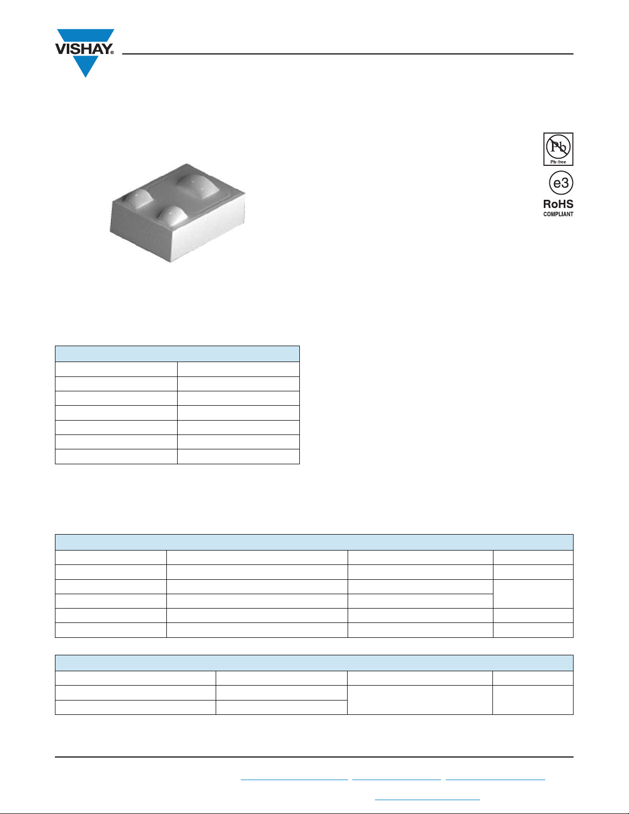
Vishay’s FlipKY® product family utilizes wafer level
chip scale packaging to deliver Schottky diodes with the
lowest VF to PCB footprint area in industry. The three pad
0.9 mm x 1.2 mm devices can deliver up to 0.75 A and
2
occupy only 1.08 mm
of board space. The anode and
cathode connections are made through solder bump pads
on one side of the silicon enabling designers to strategically
place the diodes on the PCB. This design not only minimizes
board space but also reduces thermal resistance and
inductance, which can improve overall circuit efficiency.
Typical applications include hand-held, portable equipment
such as cell phones, MP3 players, bluetooth, GPS, PDAs,
and portable hard disk drives where space savings and
performance are crucial.
MAJOR RATINGS AND CHARACTERISTICS
SYMBOL CHARACTERISTICS MAX. UNITS
DESCRIPTION
V
I
F(AV)
I
FSM
V
T
RRM
F
J
Rectangular waveform 0.75
0.75 Apk, TJ = 125 °C 0.37 V
30 V
190
- 55 to 150 °C
A
VOLTAGE RATINGS
PARAMETER SYMBOL VS-FCSP0730TR UNITS
Maximum DC reverse voltage V
Maximum working peak reverse voltage V
Revision: 04-Jul-11
For technical questions within your region: DiodesAmericas@vishay.com
THIS DOCUMENT IS SUBJECT TO CHANGE WITHOUT NOTICE. THE PRODUCTS DESCRIBED HEREIN AND THIS DOCUMENT
ARE SUBJECT TO SPECIFIC DISCLAIMERS, SET FORTH AT www.vishay.com/doc?91000
R
RWM
30 V
1
, DiodesAsia@vishay.com, DiodesEurope@vishay.com
Document Number: 94336
dP
tot
dT
J
-------------
1
R
thJA
--------------<
VS-FCSP0730TR
www.vishay.com
ABSOLUTE MAXIMUM RATINGS
PARAMETER SYMBOL TEST CONDITIONS VALUES UNITS
Maximum average forward current I
Maximum peak one cycle
non-repetitive surge current at 25 °C
Non-repetitive avalanche energy E
Repetitive avalanche current I
F(AV)
I
FSM
AR
50 % duty cycle at T
5 µs sine or 3 µs rect. pulse
10 ms sine or 6 ms rect. pulse 10
AS
TJ = 25 °C, IAS = 2.0 A, L = 5.0 mH 5mJ
Current decaying linearly to zero in 1 μs
Frequency limited by T
= 127 °C, rectangular waveform 0.75
PCB
Following any rated
load condition and with
rated V
maximum VA = 1.5 x VR typical
J
ELECTRICAL SPECIFICATIONS
PARAMETER SYMBOL TEST CONDITIONS TYP. MAX. UNITS
0.75 A
Maximum forward voltage drop
See fig. 1
V
FM
1.5 A 0.50 0.54
(1)
0.75 A
1.5 A 0.43 0.47
Maximum reverse leakage current
See fig. 2
I
RM
Maximum junction capacitance C
TJ = 25 °C
(1)
T
J
VR = 5 VDC (test signal range 100 kHz to 1 MHz), 25 °C -90pF
T
Maximum voltage rate of charge dV/dt Rated V
Note
(1)
Pulse width < 300 μs, duty cycle < 2 %
= 125 °C 515mA
R
T
= 25 °C
J
= 125 °C
T
J
V
= Rated V
R
Vishay Semiconductors
190
applied
RRM
0.5 A
0.43 0.47
0.33 0.37
R
10 50 µA
- 10 000 V/µs
A
V
THERMAL - MECHANICAL SPECIFICATIONS
PARAMETER SYMBOL TEST CONDITIONS VALUES UNITS
Maximum junction and
storage temperature range
Typical thermal resistance,
junction to PCB
Typical thermal resistance,
junction to ambient
Notes
(1)
(2)
Mounted on minimum footprint PCB
thermal runaway condition for a diode on its own heatsink
(1)
T
, T
J
Stg
(2)
R
DC operation 35
R
thJL
thJA
- 55 to 150 °C
150
°C/W
Revision: 04-Jul-11
For technical questions within your region: DiodesAmericas@vishay.com
THIS DOCUMENT IS SUBJECT TO CHANGE WITHOUT NOTICE. THE PRODUCTS DESCRIBED HEREIN AND THIS DOCUMENT
ARE SUBJECT TO SPECIFIC DISCLAIMERS, SET FORTH AT www.vishay.com/doc?91000
2
, DiodesAsia@vishay.com, DiodesEurope@vishay.com
Document Number: 94336
 Loading...