

K
VS-8STH06FP
Vishay Semiconductors
Hyperfast Rectifier, 8 A FRED Pt
3L TO-220 FULL-PA
PRODUCT SUMMARY
Package 3L TO-220FP
I
F(AV)
V
R
V
at I
F
F
t
(typ.) See Recovery table
rr
T
max. 175 °C
J
Diode variation Doubler
12
8 A
600 V
2.4 V
®
FEATURES
• Hyperfast recovery time, extremely low Qrr
• 175 °C maximum operating junction temperature
• High frequency PFC CCM operation
• Low leakage current
• Halogen-free according to IEC 61249-2-21 definition
3
• Designed and qualified for industrial level
DESCRIPTION
VS-8STH06FP 600 V series are the state of the art
tandem hyperfast recovery rectifiers: excellent switching
performance and extremely low forward voltage drop trade
off is overcome, boosting overall application performance.
Specially designed for CCM PFC application, these devices
show incomparable performance in every current intensive
hard switching application.
Optimized reverse recovery stored charge enables
downsizing of boosting switch and cooling system,
increased operating frequency make possible use of smaller
reactive elements. Cost effective PFC application is then
possible with high efficiency over wide input voltage range
and loading factor.
Plastic insulated package features easy mounting together
with not insulated parts.
ABSOLUTE MAXIMUM RATINGS FOR BOTH DIODES
PARAMETER SYMBOL TEST CONDITIONS MAX. UNITS
Repetitive peak reverse voltage V
DC forward current I
Non-repetitive peak surge current I
Operating junction and storage temperatures T
J
RRM
FSM
, T
F
50 % duty cycle, rect. waveforms, TC = 93 °C 8
TC = 25 °C 100
Stg
600 V
A
- 55 to 175 °C
ELECTRICAL SPECIFICATIONS FOR BOTH DIODES (TJ = 25 °C unless otherwise specified)
PARAMETER SYMBOL TEST CONDITIONS MIN. TYP. MAX. UNITS
Breakdown voltage,
blocking voltage
Forward voltage V
Reverse leakage current I
Junction capacitance C
,
V
BR
V
R
IR = 100 μA 600 - -
R
IF = 8 A - 2.1 2.4
I
F
T
= 8 A, TJ = 125 °C - 1.7 2
F
I
= 8 A, TJ = 150 °C - 1.6 1.8
F
VR = VR rated - < 1 10
= 125 °C, VR = VR rated - 7 80
J
T
= 150 °C, VR = VR rated - 27 100
J
VR = 600 V - 12 - pF
V
μAT
Document Number: 94554 For technical questions within your region, please contact one of the following: www.vishay.com
Revision: 19-Aug-10 DiodesAmericas@vishay.com
, DiodesAsia@vishay.com, DiodesEurope@vishay.com 1
VS-8STH06FP
Vishay Semiconductors
Hyperfast Rectifier, 8 A FRED Pt
®
DYNAMIC RECOVERY CHARACTERISTICS FOR BOTH DIODES (TJ = 25 °C unless otherwise specified)
PARAMETER SYMBOL TEST CONDITIONS MIN. TYP. MAX. UNITS
IF = 1.0 A, dIF/dt = - 50 A/μs, VR = 30 V - - 25
Reverse recovery time t
Peak recovery current I
Reverse recovery charge Q
rr
RRM
rr
= 25 °C
J
T
= 125 °C - 35 -
J
TJ = 25 °C - 2.8 -
T
= 125 °C - 4.6 5.5
J
= 8 A
I
F
dI
/dt = - 200 A/μs
F
V
= 390 V
R
-19-
TJ = 25 °C - 26 -
T
= 125 °C - 84 -
J
THERMAL - MECHANICAL SPECIFICATIONS FOR BOTH DIODES
PARAMETER SYMBOL TEST CONDITIONS MIN. TYP. MAX. UNITS
Maximum junction and
storage temperature range
Thermal resistance,
junction to case
Thermal resistance,
case to heatsink
Weight
Mounting torque
Marking device Case style 3L TO-220 FULL-PAK 8STH06FP
, T
T
J
Stg
R
thJC
R
thCS
Mounting surface, flat, smooth
and greased
- 55 - 175 °C
-4.14.8
°C/W
-0.2-
-2.0- g
-0.07- oz.
6.0
(5.0)
-
12
(10)
kgf · cm
(lbf · in)
nsT
A
nC
www.vishay.com For technical questions within your region, please contact one of the following: Document Number: 94554
2 DiodesAmericas@vishay.com
, DiodesAsia@vishay.com, DiodesEurope@vishay.com Revision: 19-Aug-10
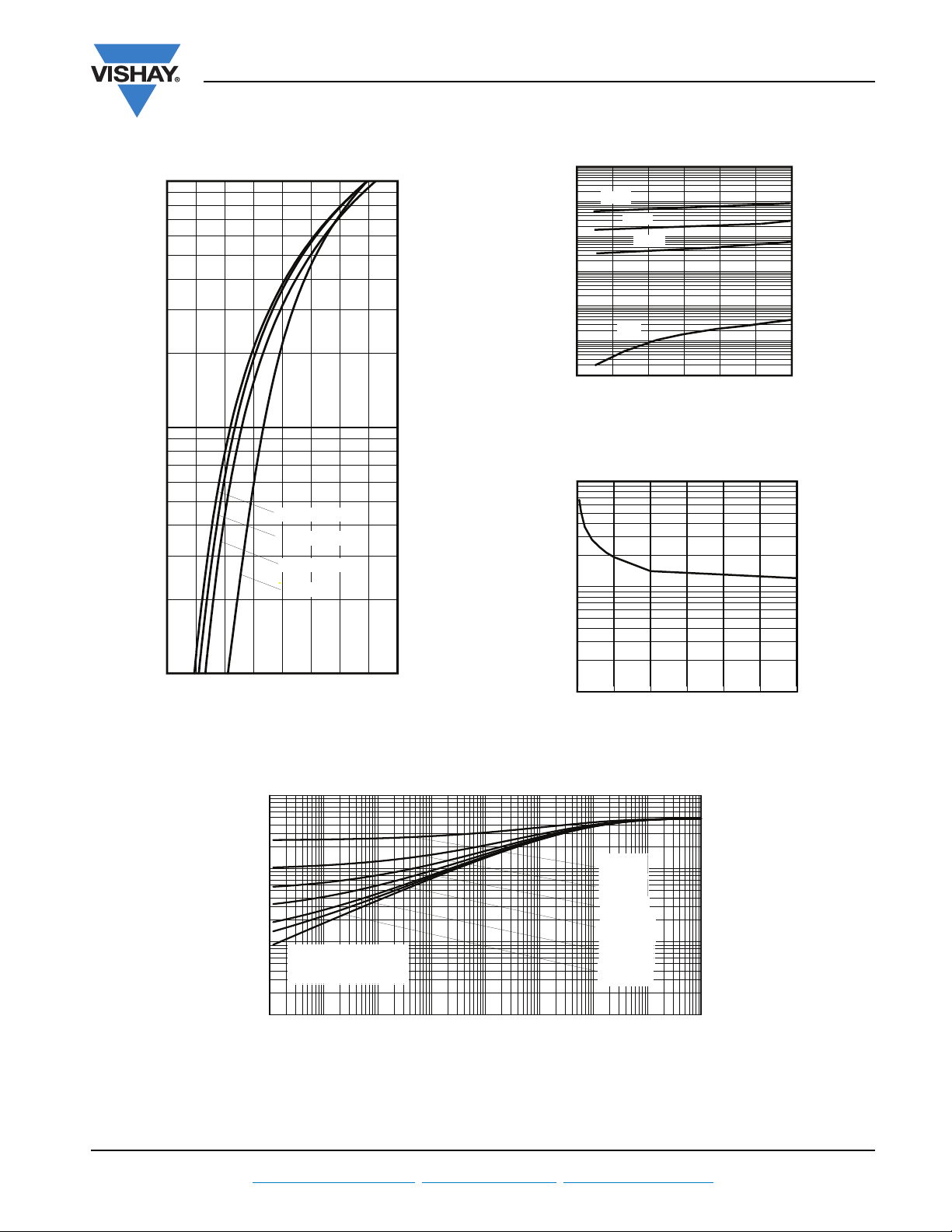
Forward Voltage Drop - VFM (V)
Instantaneous Forward Current - I
F
(A)
0.5 1.0 1.5 2.0 2.5 3.0 3.5 4.0 4.5
1
10
100
Tj = 25°C
Tj = 125°C
Tj = 175°C
Tj = 150°C
Reverse Voltage - VR (V)
Junction Capacitance - C
T
(pF)
0 100 200 300 400 500 600
1
10
100
VS-8STH06FP
Hyperfast Rectifier, 8 A FRED Pt
1000
100
(μA)
R
0.1
Reverse Current - I
0.01
0.001
175°C
10
1
0 100 200 300 400 500 600
Fig. 2 - Typical Values of Reverse Current vs.
®
Vishay Semiconductors
150°C
125°C
25°C
Reverse Voltage - VR (V)
Reverse Voltage
Fig. 1 - Maximum Forward Voltage Drop Characteristics
Fig. 3 - Typical Junction Capacitance vs. Reverse Voltage
10
(°C/W)
thJC
1
0.1
Single Pulse
(Thermal Resistance)
D = 0.5
D = 0.2
D = 0.1
D = 0.05
D = 0.02
D = 0.01
Thermal Impedance Z
0.01
1E-05 1E-04 1E-03 1E-02 1E-01 1E+00 1E+01 1E+02 1E+03
t1, Rectangular Pulse Duration (Seconds)
Fig. 4 - Maximum Thermal Impedance Z
Characteristics
thJC
Document Number: 94554 For technical questions within your region, please contact one of the following: www.vishay.com
Revision: 19-Aug-10 DiodesAmericas@vishay.com
, DiodesAsia@vishay.com, DiodesEurope@vishay.com 3

VS-8STH06FP
Average Forward Current - IF
(AV)
(A)
Allowable Case Temperature (°C)
0 2 4 6 8 10 12 14
0
50
100
150
200
DC
50% rated Vr applied
Square Wave (D = 50)
see note (1)
trr ( ns )
diF/dt (A/μs )
0001001
10
100
If = 8A, 125°C
If = 8A, 25°C
Vr = 390V
Qrr ( nC )
diF/dt (A/μs )
0001001
10
100
1000
If = 8A, 125°C
If = 8A, 25°C
Vr = 390V
Vishay Semiconductors
Fig. 5 - Maximum Allowable Case Temperature vs.
Average Forward Current
Hyperfast Rectifier, 8 A FRED Pt
25
20
15
10
5
Average Power Loss ( Watts )
0
024681012
Fig. 6 - Forward Power Loss Characteristics
®
RMS Limit
D = 0.01
D = 0.02
D = 0.05
D = 0.1
D = 0.2
D = 0.5
DC
Fig. 7 - Typical Reverse Recovery Time vs. dI
Note
(1)
Formula used: TC = TJ - (Pd +Pd
Pd = Forward power loss = I
Pd
= Inverse power loss = VR1 x IR (1 - D); IR at VR1 = 50 % rated V
REV
www.vishay.com For technical questions within your region, please contact one of the following: Document Number: 94554
4 DiodesAmericas@vishay.com
REV
x VFM at (I
F(AV)
) x R
thJC
;
F(AV)
/dt Fig. 8 - Typical Stored Charge vs. dIF/dt
F
/D) (see fig. 6);
R
, DiodesAsia@vishay.com, DiodesEurope@vishay.com Revision: 19-Aug-10

2 - Current rating (8 = 8 A)
3
- S = Doubler
4
- T = TO-220
5
- H = Hyperfast recovery
1 - Vishay Semiconductors product suffix
- Voltage rating (06 = 600 V)
6
- FP = TO-220 FULL-PAK
7
Device code
51 32 4 6 7
VS- 8 S T H 06 FP
VS-8STH06FP
Hyperfast Rectifier, 8 A FRED Pt
®
Vishay Semiconductors
ORDERING INFORMATION TABLE
LINKS TO RELATED DOCUMENTS
Dimensions www.vishay.com/doc?95264
Part marking information www.vishay.com/doc?95266
Document Number: 94554 For technical questions within your region, please contact one of the following: www.vishay.com
Revision: 19-Aug-10 DiodesAmericas@vishay.com
, DiodesAsia@vishay.com, DiodesEurope@vishay.com 5

TO-220 (3 PIN) FULL-PAK Tandem
DIMENSIONS in millimeters
Outline Dimensions
Vishay High Power Products
0.96 ± 0.051
15.9 ± 0.127
9.68 ± 0.127
R0.6 (both sides)
10.5 ± 0.127
2.54
+
0.7
13.6 ± 0.127
+ 0.076
- 0.051
Ø 3.40 ± 0.051
7.5° (2 pics)
+ 0.127
0.5
- 0.051
4.69 ± 0.127
2.7 ± 0.127
2.56 ± 0.051
Ø 3.0 ± 0.051
0.96 ± 0.051
3.3 ± 0.127
6.4 ± 0.051
Ø 1.78
3.2 ± 0.051
11.16 ± 0.051
Ø 1.50
5°
Document Number: 95264 For technical questions concerning discrete products, contact: diodes-tech@vishay.com
Revision: 21-Jul-08 For technical questions concerning module products, contact: ind-modules@vishay.com
www.vishay.com
1

Legal Disclaimer Notice
Vishay
Disclaimer
ALL PRODUCT, PRODUCT SPECIFICATIONS AND DATA ARE SUBJECT TO CHANGE WITHOUT NOTICE TO IMPROVE
RELIABILITY, FUNCTION OR DESIGN OR OTHERWISE.
Vishay Intertechnology, Inc., its affiliates, agents, and employees, and all persons acting on its or their behalf (collectively,
“Vishay”), disclaim any and all liability for any errors, inaccuracies or incompleteness contained in any datasheet or in any other
disclosure relating to any product.
Vishay makes no warranty, representation or guarantee regarding the suitability of the products for any particular purpose or
the continuing production of any product. To the maximum extent permitted by applicable law, Vishay disclaims (i) any and all
liability arising out of the application or use of any product, (ii) any and all liability, including without limitation special,
consequential or incidental damages, and (iii) any and all implied warranties, including warranties of fitness for particular
purpose, non-infringement and merchantability.
Statements regarding the suitability of products for certain types of applications are based on Vishay’s knowledge of typical
requirements that are often placed on Vishay products in generic applications. Such statements are not binding statements
about the suitability of products for a particular application. It is the customer’s responsibility to validate that a particular
product with the properties described in the product specification is suitable for use in a particular application. Parameters
provided in datasheets and/or specifications may vary in different applications and performance may vary over time. All
operating parameters, including typical parameters, must be validated for each customer application by the customer’s
technical experts. Product specifications do not expand or otherwise modify Vishay’s terms and conditions of purchase,
including but not limited to the warranty expressed therein.
Except as expressly indicated in writing, Vishay products are not designed for use in medical, life-saving, or life-sustaining
applications or for any other application in which the failure of the Vishay product could result in personal injury or death.
Customers using or selling Vishay products not expressly indicated for use in such applications do so at their own risk and agree
to fully indemnify and hold Vishay and its distributors harmless from and against any and all claims, liabilities, expenses and
damages arising or resulting in connection with such use or sale, including attorneys fees, even if such claim alleges that Vishay
or its distributor was negligent regarding the design or manufacture of the part. Please contact authorized Vishay personnel to
obtain written terms and conditions regarding products designed for such applications.
No license, express or implied, by estoppel or otherwise, to any intellectual property rights is granted by this document or by
any conduct of Vishay. Product names and markings noted herein may be trademarks of their respective owners.
Document Number: 91000 www.vishay.com
Revision: 11-Mar-11 1
 Loading...