Vishay VS-8EWS..SPbF Series Data Sheet

VS-8EWS..SPbF Series
A
1
2
3
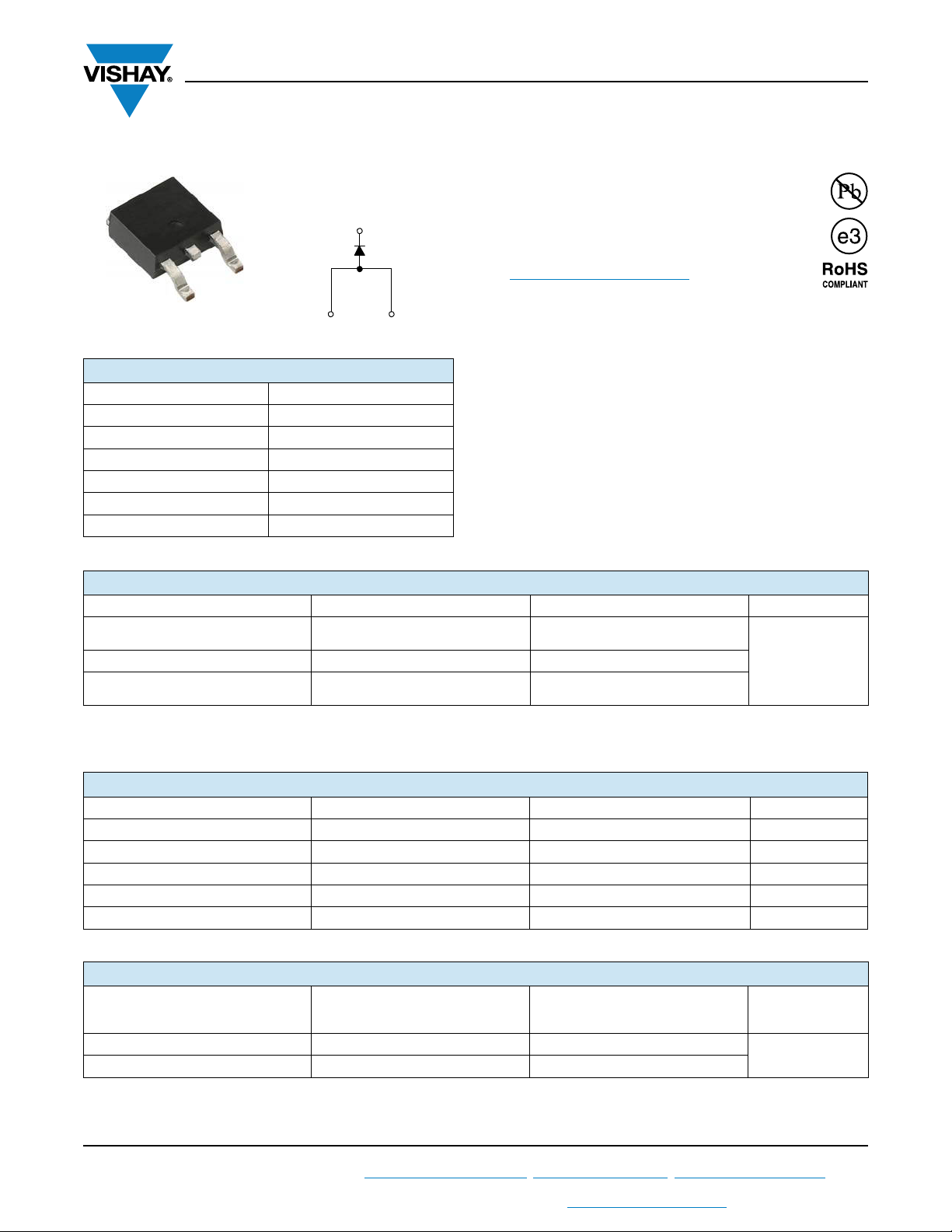
D-PAK
www.vishay.com
Vishay Semiconductors
High Voltage Surface Mount Input Rectifier Diode, 8 A
FEATURES
Base
cathode
+
2
• Meets MSL level 1, per J-STD-020, LF maximum
peak of 260 °C
• Material categorization:
For definitions of compliance please see
www.vishay.com/doc?99912
13
--
node
Anode
APPLICATIONS
• Input rectification
• Vishay Semiconductors switches and output rectifiers
PRODUCT SUMMARY
Package D-PAK (TO-252AA)
I
F(AV)
V
R
V
at I
F
F
I
FSM
T
max. 150 °C
J
Diode variation Single die
8 A
800 V, 1200 V
1.1 V
150 A
which are available in identical package outlines
DESCRIPTION
The 8EWS..SPbF rectifier high voltage series has been
optimized for very low forward voltage drop, with moderate
leakage. The glass passivation technology used has reliable
operation up to 150 °C junction temperature.
The high reverse voltage range available allows design of
input stage primary rectification with outstanding voltage
surge capability.
OUTPUT CURRENT IN TYPICAL APPLICATIONS
APPLICATIONS SINGLE-PHASE BRIDGE THREE-PHASE BRIDGE UNITS
NEMA FR-4 or G10 glass fabric-based
epoxy with 4 oz. (140 μm) copper
= 15 °C/W 2.5 2.8
thCA
Aluminum IMS with heatsink,
= 5 °C/W
R
thCA
Note
= 55 °C, TJ = 125 °C, footprint 300 mm
•T
A
2
1.2 1.6
5.5 6.5
AAluminum IMS, R
MAJOR RATINGS AND CHARACTERISTICS
SYMBOL CHARACTERISTICS VALUES UNITS
I
F(AV)
V
I
FSM
V
T
RRM
F
J
Sinusoidal waveform at TC = 116 °C 8 A
800/1200 V
150 A
8 A, TJ = 25 °C 1.10 V
-55 to 150 °C
VOLTAGE RATINGS
PART NUMBER
8EWS08SPbF 800 900
8EWS12SPbF 1200 1300
Revision: 18-Dec-13
For technical questions within your region: DiodesAmericas@vishay.com
THIS DOCUMENT IS SUBJECT TO CHANGE WITHOUT NOTICE. THE PRODUCTS DESCRIBED HEREIN AND THIS DOCUMENT
ARE SUBJECT TO SPECIFIC DISCLAIMERS, SET FORTH AT www.vishay.com/doc?91000
PEAK REVERSE VOLTAGE
V
1
, MAXIMUM
V
RRM
V
, MAXIMUM NON-REPETITIVE
RSM
PEAK REVERSE VOLTAGE
, DiodesAsia@vishay.com, DiodesEurope@vishay.com
V
Document Number: 94349
I
RRM
AT 150 °C
mA
0.5

VS-8EWS..SPbF Series
www.vishay.com
ABSOLUTE MAXIMUM RATINGS
PARAMETER SYMBOL TEST CONDITIONS VALUES UNITS
Maximum average forward current I
Maximum peak one cycle
non-repetitive surge current
Maximum I
Maximum I
2
t for fusing I2t
2
t for fusing I2t t = 0.1 ms to 10 ms, no voltage reapplied 1100 A2s
F(AV)
I
FSM
TC = 105 °C, 180° conduction half sine wave 8
10 ms sine pulse, rated V
applied 125
RRM
10 ms sine pulse, no voltage reapplied 150
10 ms sine pulse, rated V
applied 78
RRM
10 ms sine pulse, no voltage reapplied 110
ELECTRICAL SPECIFICATIONS
PARAMETER SYMBOL TEST CONDITIONS VALUES UNITS
Maximum forward voltage drop V
Forward slope resistance r
Threshold voltage V
Maximum reverse leakage current I
FM
F(TO)
RM
8 A, TJ = 25 °C 1.1 V
t
TJ = 150 °C
TJ = 25 °C
T
= 150 °C 0.50
J
V
= Rated V
R
Vishay Semiconductors
20 m
0.82 V
0.05
RRM
A
A
mA
2
s
THERMAL - MECHANICAL SPECIFICATIONS
PARAMETER SYMBOL TEST CONDITIONS VALUES UNITS
Maximum junction and storage
temperature range
Soldering temperature T
Maximum thermal resistance,
junction to case
Typical thermal resistance,
junction to ambient (PCB mount)
Approximate weight
Marking device Case style D-PAK (TO-252AA) 8EWS12S
Note
(1)
When mounted on 1" square (650 mm2) PCB of FR-4 or G-10 material 4 oz. (140 μm) copper 40 °C/W
For recommended footprint and soldering techniques refer to application note #AN-994
, T
T
J
Stg
S
DC operation 2.5
R
thJC
62
R
thJA (1)
-55 to 150
260
1g
0.03 oz.
°C
°C/W
Revision: 18-Dec-13
For technical questions within your region: DiodesAmericas@vishay.com
THIS DOCUMENT IS SUBJECT TO CHANGE WITHOUT NOTICE. THE PRODUCTS DESCRIBED HEREIN AND THIS DOCUMENT
ARE SUBJECT TO SPECIFIC DISCLAIMERS, SET FORTH AT www.vishay.com/doc?91000
2
, DiodesAsia@vishay.com, DiodesEurope@vishay.com
Document Number: 94349

www.vishay.com
90
80
130
140
150
120
110
100
Maximum Allowable Case
Temperature (°C)
Average Forward Current (A)
2
10
12
468
0
30°
60°
90°
120°
180°
8EWS. Series
R
thJC
(DC) = 2.5 °C/W
90
140
150
130
120
110
100
Maximum Allowable Case
Temperature (°C)
Average Forward Current (A)
4268
16
18
10 12 14
0
DC
30°
60°
90°
120°
180°
8EWS. Series
R
thJC
(DC) = 2.5 °C/W
Ø
Conduction period
8
6
4
2
0
10
12
14
16
Maximum Average Forward
Power Loss (W)
Average Forward Current (A)
4268
10
0
RMS limit
180°
120°
90°
60°
30°
8EWS. Series
T
J
= 150 °C
Conduction angle
Ø
8
6
4
2
0
10
12
14
16
18
20
Maximum Average Forward
Power Loss (W)
Average Forward Current (A)
246
14
16
81012
0
DC
180°
120°
90°
60°
30°
RMS limit
8EWS. Series
T
J
= 150 °C
Ø
Conduction period
Peak Half Sine Wave
Forward Current (A)
Number of Equal Amplitude
Half Cycle Current Pulses (N)
110100
30
40
50
60
70
80
90
100
110
120
130
140
VS-8EWS08S .. Series
At any rated load condition and with
rated V
rrm
applied following surge.
Initial T
J
= 150 °C
at 60 Hz 0.0083 s
at 50 Hz 0.0100 s
Peak Half Sine Wave
Forward Current (A)
Pulse Train Duration (s)
0.01 0.1 1 10
20
40
60
80
100
120
140
160
Maximum non-repetitive surge current
versus pulse train duration.
Initial T
J
= TJ max.
No voltage reapplied
Rated V
rrm
reapplied
VS-8EWS08S .. Series
VS-8EWS..SPbF Series
Vishay Semiconductors
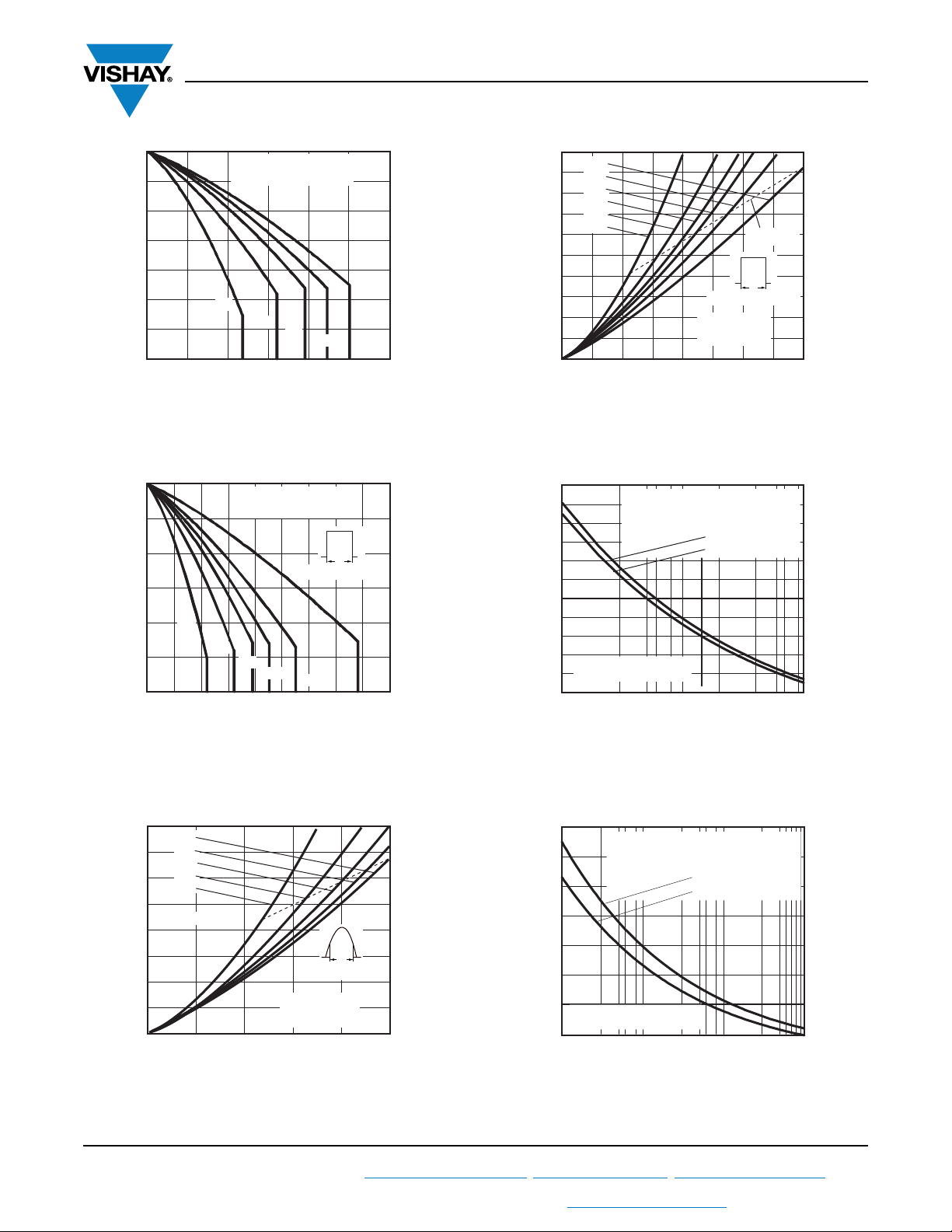
Fig. 1 - Current Rating Characteristics
Fig. 2 - Current Rating Characteristics
Fig. 4 - Forward Power Loss Characteristics
Fig. 5 - Maximum Non-Repetitive Surge Current
Fig. 3 - Forward Power Loss Characteristics
Revision: 18-Dec-13
For technical questions within your region: DiodesAmericas@vishay.com
THIS DOCUMENT IS SUBJECT TO CHANGE WITHOUT NOTICE. THE PRODUCTS DESCRIBED HEREIN AND THIS DOCUMENT
Fig. 6 - Maximum Non-Repetitive Surge Current
ARE SUBJECT TO SPECIFIC DISCLAIMERS, SET FORTH AT www.vishay.com/doc?91000
3
, DiodesAsia@vishay.com, DiodesEurope@vishay.com
Document Number: 94349
 Loading...