Vishay VS-80EBU02 Data Sheet

www.vishay.com
Cathode Anode
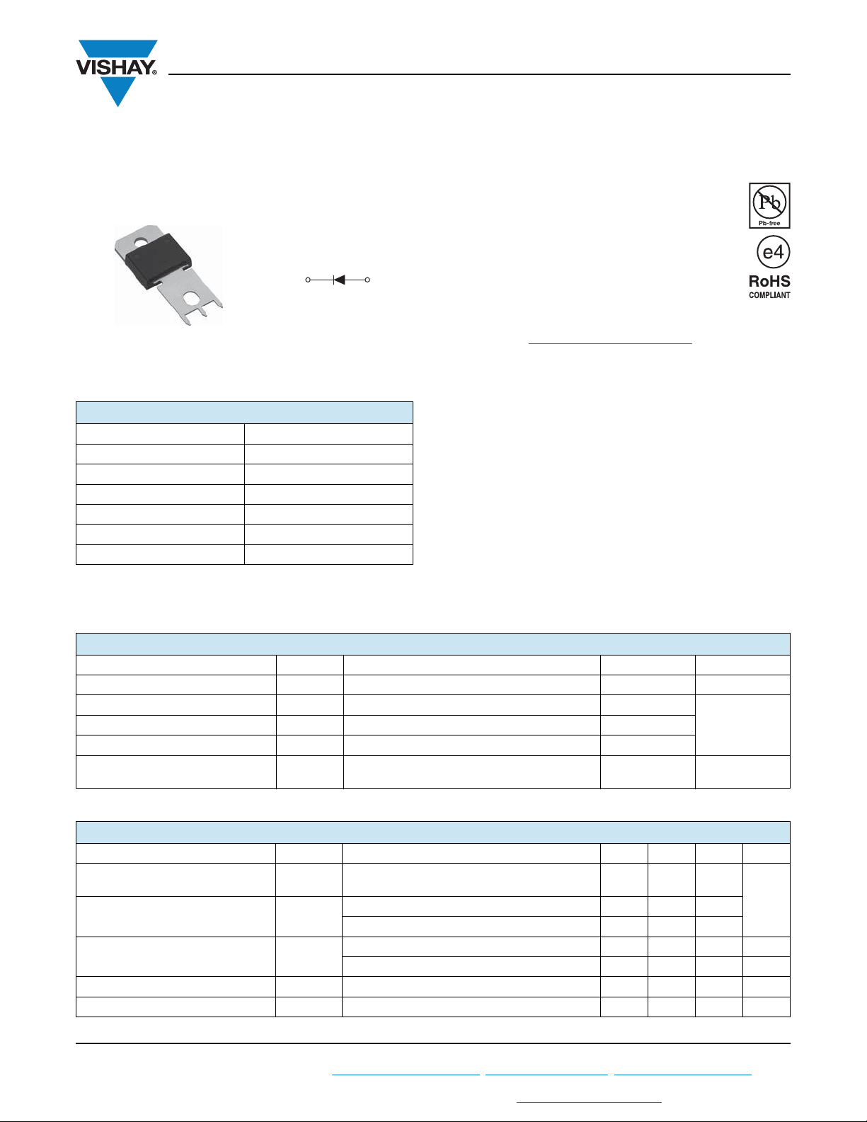
PowerTab
®
VS-80EBU02
Vishay Semiconductors
Ultrafast Soft Recovery Diode, 80 A FRED Pt
PRODUCT SUMMARY
Package PowerTab
I
F(AV)
V
R
V
at I
F
F
(typ.) See recovery table
t
rr
T
max. 175 °C
J
Diode variation Single die
80 A
200 V
1.13 V
®
FEATURES
• Ultrafast recovery time
• 175 °C max. operating junction temperature
• Screw mounting only
• Designed and qualified according to
JEDEC-JESD47
• PowerTab
• Material categorization: For definitions of compliance
please see www.vishay.com/doc?99912
BENEFITS
• Reduced RFI and EMI
• Higher frequency operation
®
• Reduced snubbing
• Reduced parts count
DESCRIPTION/APPLICATIONS
These diodes are optimized to reduce losses and EMI/RFI in
high frequency power conditioning systems.
The softness of the recovery eliminates the need for a
snubber in most applications. These devices are ideally
suited for HF welding, power converters and other
applications where switching losses are not significant
portion of the total losses.
®
package
ABSOLUTE MAXIMUM RATINGS
PARAMETER SYMBOL TEST CONDITIONS MAX. UNITS
Cathode to anode voltage V
Continuous forward current I
Maximum repetitive forward current I
Operating junction and
storage temperatures
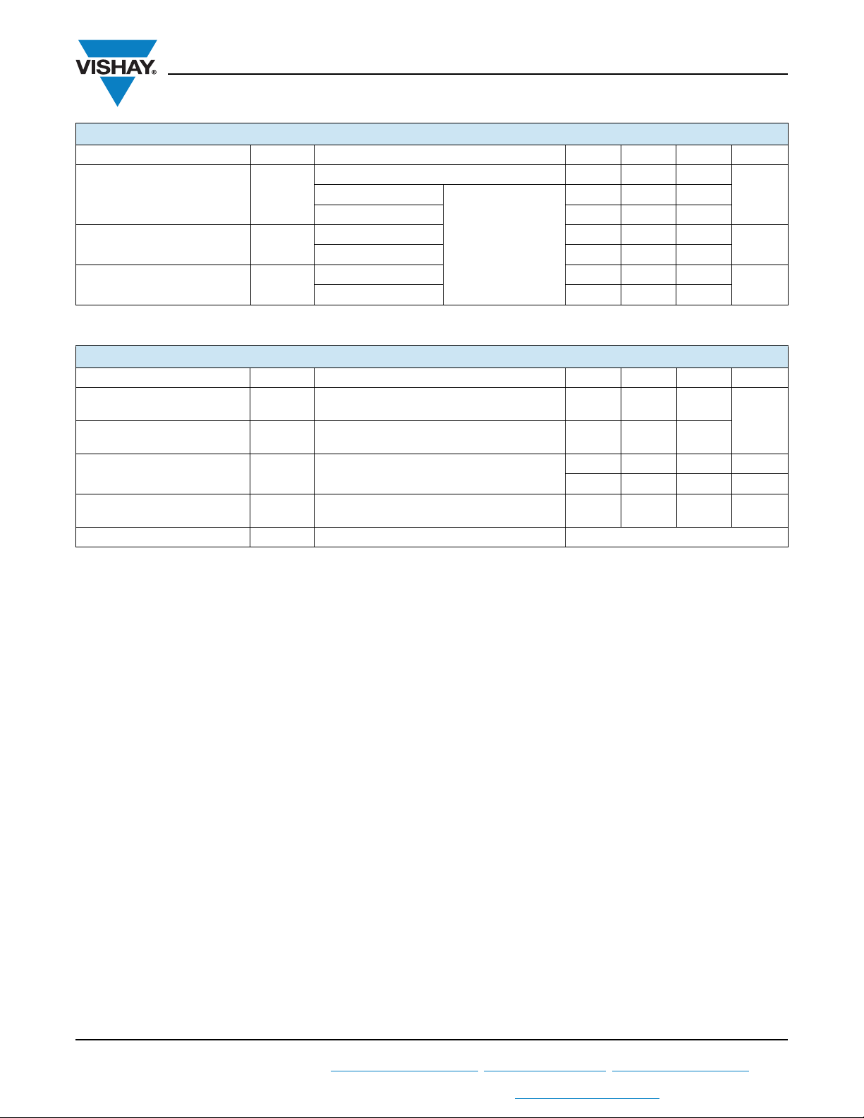
ELECTRICAL SPECIFICATIONS (TJ = 25 °C unless otherwise specified)
PARAMETER SYMBOL TEST CONDITIONS MIN. TYP. MAX. UNITS
Breakdown voltage,
blocking voltage
Forward voltage V
Reverse leakage current I
Junction capacitance C
Series inductance L
Revision: 11-Dec-12
R
F(AV)
FSM
FRM
T
, T
J
V
BR
V
r
F
R
T
S
For technical questions within your region: DiodesAmericas@vishay.com
THIS DOCUMENT IS SUBJECT TO CHANGE WITHOUT NOTICE. THE PRODUCTS DESCRIBED HEREIN AND THIS DOCUMENT
ARE SUBJECT TO SPECIFIC DISCLAIMERS, SET FORTH AT www.vishay.com/doc?91000
TC = 112 °C 80
TC = 25 °C 800
Square wave, 20 kHz 160
Stg
,
IR = 50 μA 200 - -
IF = 80 A - 0.98 1.13
I
= 80 A, TJ = 175 °C - 0.79 0.92
F
VR = VR rated - - 50 μA
T
= 150 °C, VR = VR rated - - 2 mA
J
VR = 200 V - 89 - pF
Measured lead to lead 5 mm from package body - 3.5 - nH
1
, DiodesAsia@vishay.com, DiodesEurope@vishay.com
200 V
ASingle pulse forward current I
- 55 to 175 °C
Document Number: 93024
V

VS-80EBU02
www.vishay.com
DYNAMIC RECOVERY CHARACTERISTICS (TJ = 25 °C unless otherwise specified)
PARAMETER SYMBOL TEST CONDITIONS MIN. TYP. MAX. UNITS
IF = 1.0 A, dIF/dt = 200 A/μs, VR = 30 V - - 35
Reverse recovery time t
Peak recovery current I
Reverse recovery charge Q
rr
RRM
rr
= 25 °C
J
= 125 °C - 52 -
T
J
TJ = 25 °C - 4.4 -
T
= 125 °C - 8.8 -
J
= 80 A
I
F
= 160 V
V
R
dI
/dt = 200 A/μs
F
TJ = 25 °C - 70 -
T
= 125 °C - 240 -
J
THERMAL - MECHANICAL SPECIFICATIONS
PARAMETER SYMBOL TEST CONDITIONS MIN. TYP. MAX. UNITS
Thermal resistance,
junction to case
Thermal resistance,
junction to heatsink
Weight
Mounting torque
Marking device Case style PowerTab® 80EBU02
- - 0.70
R
thJC
Mounting surface, flat, smooth and greased - 0.2 -
R
thCS
Vishay Semiconductors
-32-
- - 5.02 g
-0.18- oz.
1.2
(10)
-
2.4
(20)
nsT
A
nC
°C/W
N · m
(lbf · in)
Revision: 11-Dec-12
For technical questions within your region: DiodesAmericas@vishay.com
2
, DiodesAsia@vishay.com, DiodesEurope@vishay.com
Document Number: 93024
THIS DOCUMENT IS SUBJECT TO CHANGE WITHOUT NOTICE. THE PRODUCTS DESCRIBED HEREIN AND THIS DOCUMENT
ARE SUBJECT TO SPECIFIC DISCLAIMERS, SET FORTH AT www.vishay.com/doc?91000

www.vishay.com
V
FM -
Forward Voltage Drop (V)
I
F
-
Instantaneous Forward Current (A)
1
10
100
1000
0 0.5 1 1.5 2 2.5
TJ = 175 °C
T
J
= 125 °C
T
J
= 25 °C
C
T
-
Junction Capacitance (pF)
VR - Reverse Voltage (V)
10
100
1000
10 000
1 10 100 1000
TJ = 25 °C
t1 - Rectangular Pulse Duration (s)
Z
thJC
-
Thermal Impedance (°C/W)
0.01
0.1
1
0.00001 0.0001 0.001 0.01 0.1 1 10
Single Pulse
(Thermal Resistance)
D = 0.50
D = 0.20
D = 0.10
D = 0.05
D = 0.02
D = 0.01
2
t
1
t
P
DM
Notes:
1. Duty factor D = t1/ t2
2. Peak Tj = Pdm x ZthJC + Tc
VS-80EBU02
Vishay Semiconductors
1000
100
10
1
0.1
- Reverse Current (mA)
0.01
R
I
0.001
0 50 100 150 200
TJ = 175 °C
125 °C
25 °C
VR - Reverse Voltage (V)
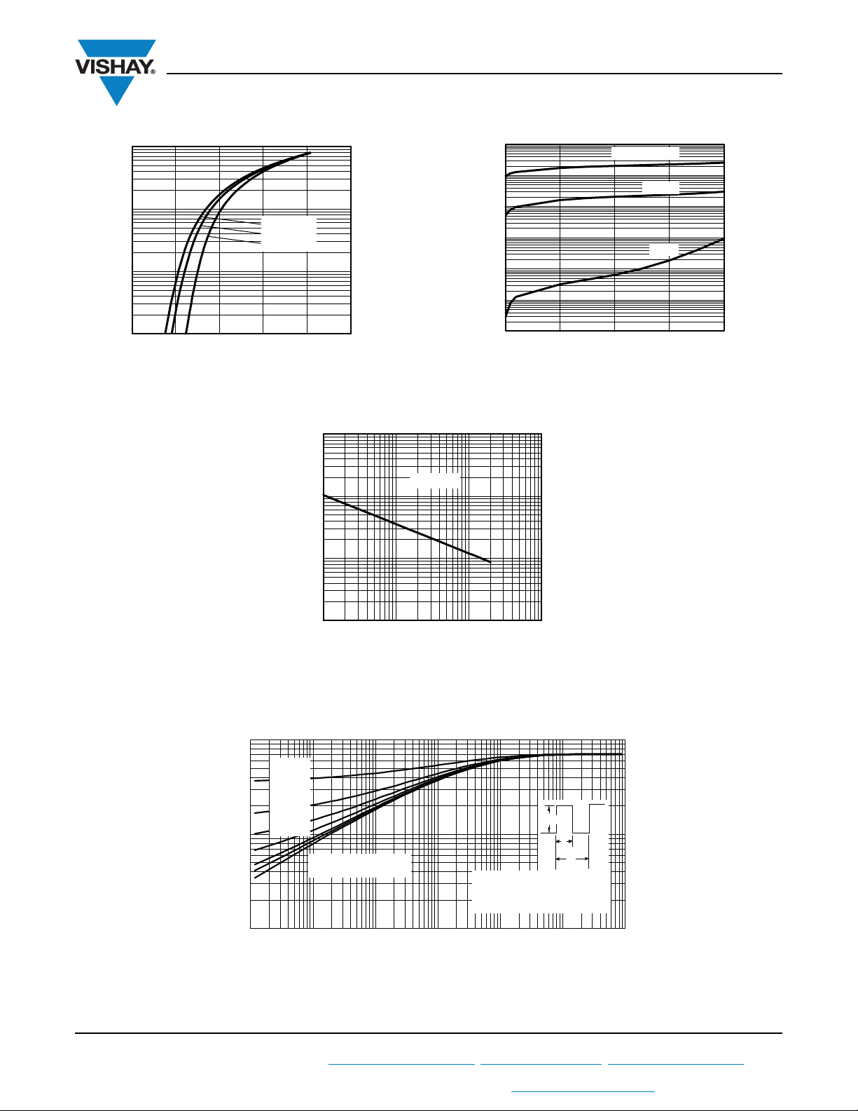
Fig. 1 - Maximum Forward Voltage Drop Characteristics Fig. 2 - Typical Values of Reverse Current vs.
Reverse Voltage
Fig. 3 - Typical Junction Capacitance vs.
Revision: 11-Dec-12
For technical questions within your region: DiodesAmericas@vishay.com
Fig. 4 - Maximum Thermal Impedance Z
THIS DOCUMENT IS SUBJECT TO CHANGE WITHOUT NOTICE. THE PRODUCTS DESCRIBED HEREIN AND THIS DOCUMENT
ARE SUBJECT TO SPECIFIC DISCLAIMERS, SET FORTH AT www.vishay.com/doc?91000
Reverse Voltage
3
Characteristics
thJC
Document Number: 93024
, DiodesAsia@vishay.com, DiodesEurope@vishay.com
 Loading...