Vishay VS-6CUT04, VS-6CWT04FN Data Sheet

High Performance Schottky Generation 5.0, 2 x 3 A
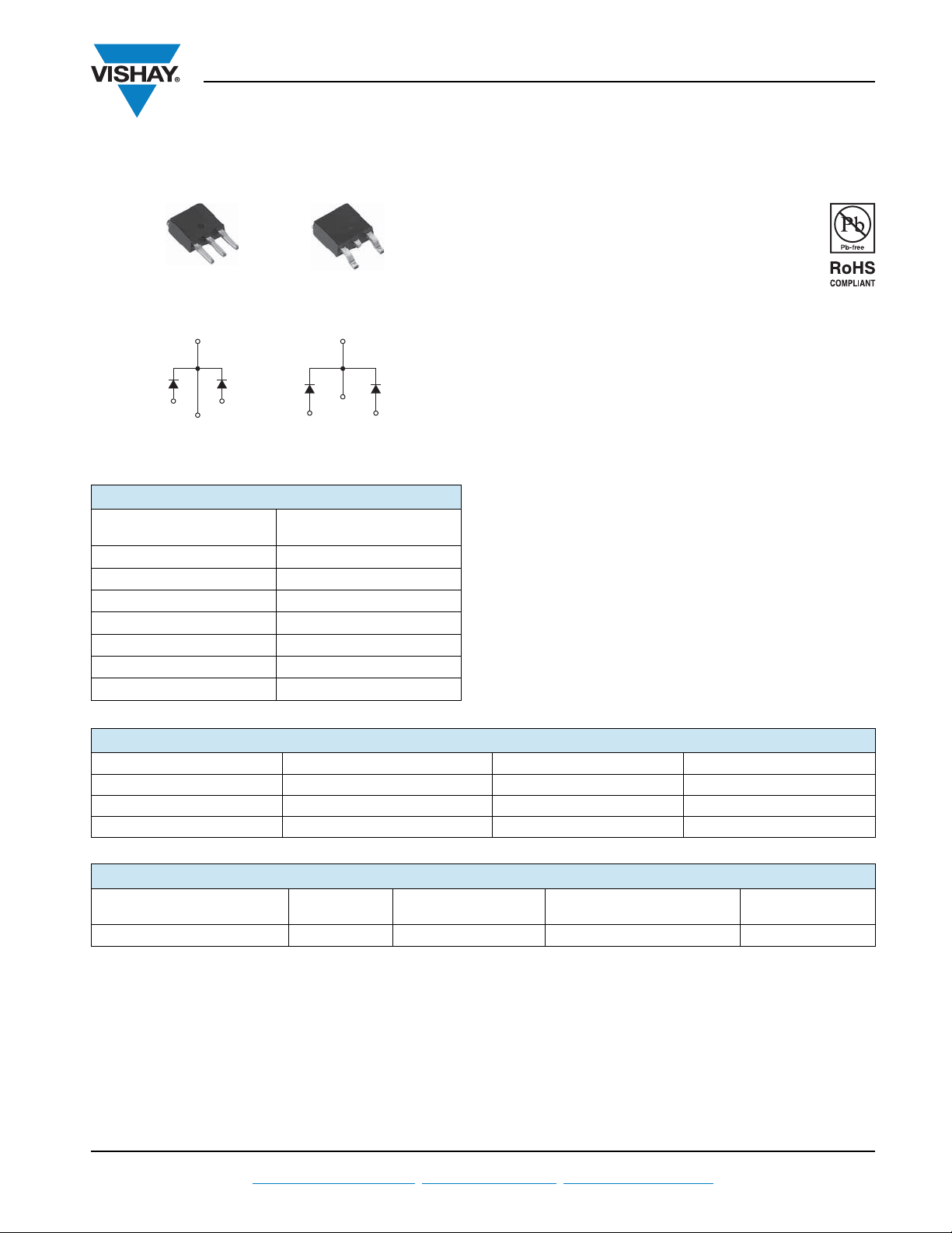
I-PAK (TO-251AA)
D-PAK (TO-252AA)
VS-6CUT04 VS-6CWT04FN
Base
common
cathode
Anode Anode
Common
cathode
4
3
2
1
Base
common
cathode
Anode Anode
Common
cathode
4
3
2
1
PRODUCT SUMMARY
Package
I
F(AV)
V
R
V
at I
F
F
I
max. 3 mA at 125 °C
RM
T
max. 175 °C
J
Diode variation Common cathode
E
AS
D-PAK (TO-252AA),
I-PAK (TO-251AA)
2 x 3 A
45 V
0.54 V
14 mJ
VS-6CUT04, VS-6CWT04FN
Vishay Semiconductors
FEATURES
• 175 °C high performance Schottky diode
• Very low forward voltage drop
• Extremely low reverse leakage
• Optimized V
• Increased ruggedness for reverse avalanche capability
• RBSOA available
• Negligible switching losses
• Submicron trench technology
• Compliant to RoHS Directive 2002/95/EC
APPLICATIONS
• Specific for PV cells pybass diode
• High efficiency SMPS
• High frequency switching
• Output rectification
• Reverse battery protection
• Freewheeling
• DC/DC systems
• Increased power density systems
vs. IR trade off for high efficiency
F
MAJOR RATINGS AND CHARACTERISTICS
SYMBOL CHARACTERISTICS VALUES UNITS
V
RRM
V
F
T
J
VOLTAGE RATINGS
PARAMETER SYMBOL TEST CONDITIONS
Maximum DC reverse voltage V
Document Number: 94650 For technical questions within your region, please contact one of the following: www.vishay.com
Revision: 04-Jan-11 DiodesAmericas@vishay.com
45 V
3 Apk, TJ = 125 °C (typical, per leg) 0.46 V
Range - 55 to 175 °C
VS-6CUT04
VS-6CWT04FN
R
TJ = 25 °C 45 V
, DiodesAsia@vishay.com, DiodesEurope@vishay.com 1
UNITS

VS-6CUT04, VS-6CWT04FN
Vishay Semiconductors
High Performance Schottky
Generation 5.0, 2 x 3 A
ABSOLUTE MAXIMUM RATINGS
PARAMETER SYMBOL TEST CONDITIONS VALUES UNITS
Maximum average
forward current
Maximum peak one cycle
non-repetitive surge current per leg
Non-repetitive avalanche
energy per leg
per leg
per device 6
I
F(AV)
I
FSM
E
50 % duty cycle at TC = 166 °C, rectangular waveform
5 μs sine or 3 μs rect. pulse
Following any rated load
condition and with rated
10 ms sine or 6 ms rect. pulse 70
TJ = 25 °C, IAS = 1.3 A, L = 16 mH 14 mJ
AS
V
RRM
applied
Limited by frequency of operation and time pulse duration
Repetitive avalanche current per leg I
AR
so that T
< TJ max. IAS at TJ max. as a function of time pulse
J
(see fig. 8)
ELECTRICAL SPECIFICATIONS
PARAMETER SYMBOL TEST CONDITIONS TYP. MAX. UNITS
3 A
Forward voltage drop per leg V
FM
(1)
3 A
6 A 0.615 0.680
6 A 0.570 0.640
Reverse leakage current per leg I
Junction capacitance per leg C
Series inductance per leg L
RM
T
J
VR = 5 VDC (test signal range 100 kHz to 1 MHz), 25 °C 240 - pF
T
Measured lead to lead 5 mm from package body 8.0 - nH
S
TJ = 25 °C
(1)
Maximum voltage rate of change dV/dt Rated V
Note
(1)
Pulse width < 300 μs, duty cycle < 2 %
= 125 °C - 3 mA
R
T
= 25 °C
J
= 125 °C
T
J
V
= Rated VR
R
3
440
I
at
AS
T
max.
J
0.535 0.600
0.485 0.540
-25μA
- 10 000 V/μs
A
A
A
V
THERMAL - MECHANICAL SPECIFICATIONS
PARAMETER SYMBOL TEST CONDITIONS VALUES UNITS
Maximum junction and
storage temperature range
Maximum thermal resistance,
junction to case per leg
Maximum thermal resistance,
junction to case per device
Typical thermal resistance,
case to heatsink
Approximate weight
Marking device
www.vishay.com For technical questions within your region, please contact one of the following: Document Number: 94650
2 DiodesAmericas@vishay.com
T
, T
J
Stg
R
DC operation
thJC
R
thCS
- 55 to 175 °C
4.7
2.35
0.3
0.3 g
0.01 oz.
Case style I-PAK 6CUT04
Case style D-PAK 6CWT04FN
, DiodesAsia@vishay.com, DiodesEurope@vishay.com Revision: 04-Jan-11
°C/W

Forward Voltage Drop - VFM (V)
Instantaneous Forward Current - I
F
(A)
0.0 0.2 0.4 0.6 0.8 1.0 1.2 1.4 1.6
0.1
1
10
100
Tj = 25°C
Tj = 125°C
Tj = 175°C
Reverse Current - I
R
(mA)
Reverse Voltage - VR (V)
0 5 10 15 20 25 30 35 40 45
0.0001
0.001
0.01
0.1
1
10
75°C
100°C
50°C
125°C
150°C
175°C
25°C
t1, Rectangular Pulse Duration (Seconds)
Thermal Impedance ZthJC (°C/W)
1E-05 1E-04 1E-03 1E-02 1E-01 1E+00
0.01
0.1
1
10
Single Pulse
(Thermal Resistance)
D = 0.2
D = 0.25
D = 0.33
D = 0.5
D = 0.75
VS-6CUT04, VS-6CWT04FN
High Performance Schottky
Generation 5.0, 2 x 3 A
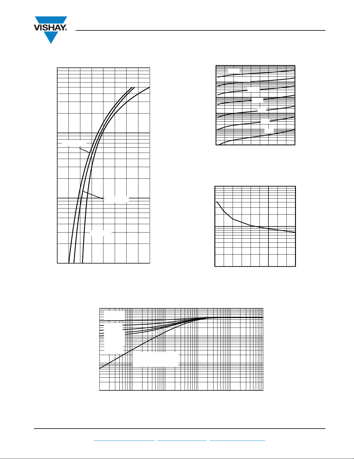
Fig. 2 - Typical Values of Reverse Current vs.
1000
Vishay Semiconductors
Reverse Voltage
Fig. 1 - Maximum Forward Voltage Drop Characteristics
Document Number: 94650 For technical questions within your region, please contact one of the following: www.vishay.com
Revision: 04-Jan-11 DiodesAmericas@vishay.com
Fig. 4 - Maximum Thermal Impedance Z
, DiodesAsia@vishay.com, DiodesEurope@vishay.com 3
(pF)
T
100
Junction Capacitance - C
10
0 5 10 15 20 25 30 35 40 45
Reverse Voltage - VR (V)
Fig. 3 - Typical Junction Capacitance vs.
Characteristics
thJC
Reverse Voltage
 Loading...