

VS-5.MT...KPbF, VS-9.MT...KPbF, VS-11.MT...KPbF Series
MT-K
K
www.vishay.com
Three Phase Controlled Bridge (Power Modules),
PRODUCT SUMMARY
I
O
V
RRM
Package MT-K
Circuit Three phase bridge
MT-
55 A to 110 A
800 V to 1600 V
55 A to 110 A
FEATURES
• Package fully compatible with the industry
standard INT-A-PAK power modules series
• High thermal conductivity package, electrically
insulated case
• Excellent power volume ratio
• 4000 V
• UL E78996 approved
• Designed and qualified for industrial level
• Material categorization: For definitions of compliance
please see www.vishay.com/doc?99912
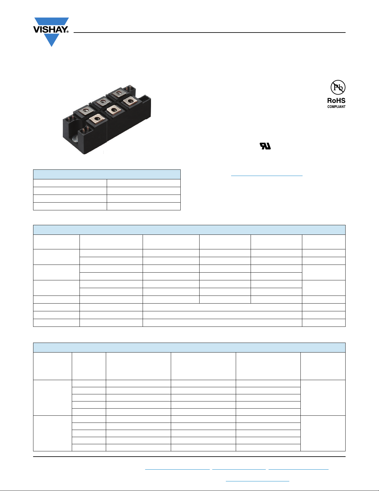
DESCRIPTION
A range of extremely compact, encapsulated three phase
controlled bridge rectifiers offering efficient and reliable
operation. They are intended for use in general purpose and
heavy duty applications.
isolating voltage
RMS
Vishay Semiconductors
MAJOR RATINGS AND CHARACTERISTICS
SYMBOL CHARACTERISTICS
I
O
I
FSM
2
t
I
2
t 7700 45 250 63 800 A2s
I
V
RRM
T
Stg
T
J
T
C
50 Hz 390 950 1130
60 Hz 410 1000 1180
50 Hz 770 4525 6380
60 Hz 700 4130 5830
Range 800 to 1600 V
Range -40 to 125 °C
Range -40 to 125 °C
VALUES
5.MT...K
55 90 110 A
85 85 85 °C
VALUES
9.MT...K
VALUES
11.MT...K
UNITS
A
A2s
ELECTRICAL SPECIFICATIONS
VOLTAGE RATINGS
V
, MAXIMUM
V
, MAXIMUM
TYPE
NUMBER
VS-5.MT...K
VS-9.MT...K
VS-11.MT...K
Revision: 27-Feb-14
For technical questions within your region: DiodesAmericas@vishay.com
THIS DOCUMENT IS SUBJECT TO CHANGE WITHOUT NOTICE. THE PRODUCTS DESCRIBED HEREIN AND THIS DOCUMENT
VOLTAGE
CODE
80 800 900 800
100 1000 1100 1000
120 1200 1300 1200
140 1400 1500 1400
160 1600 1700 1600
80 800 900 800
100 1000 1100 1000
120 1200 1300 1200
140 1400 1500 1400
160 1600 1700 1600
ARE SUBJECT TO SPECIFIC DISCLAIMERS, SET FORTH AT www.vishay.com/doc?91000
RRM
REPETITIVE PEAK
REVERSE VOLTAGE
V
V
, MAXIMUM
RSM
NON-REPETITIVE PEAK
REVERSE VOLTAGE
V
1
, DiodesAsia@vishay.com, DiodesEurope@vishay.com
DRM
REPETITIVE PEAK
OFF-STATE VOLTAGE,
GATE OPEN CIRCUIT
V
Document Number: 94353
AT TJ = 125 °C
I
RRM/IDRM
MAXIMUM
mA
10
20
,
VS-5.MT...KPbF, VS-9.MT...KPbF, VS-11.MT...KPbF Series
www.vishay.com
FORWARD CONDUCTION
PARAMETER SYMBOL TEST CONDITIONS
Maximum DC output current at
case temperature
Maximum peak, one-cycle
forward, non-repetitive on state
surge current
Maximum I
Maximum I
Low level value of threshold
voltage
High level value of threshold
voltage
2
t for fusing I2t
2
t for fusing I2t t = 0.1 ms to 10 ms, no voltage reapplied 7700 45 250 63 800 A2s
V
V
Low level value on-state slope
resistance
High level value on-state slope
resistance
Maximum on-state voltage drop V
Maximum non-repetitve
rate of rise of turned on current
Maximum holding current I
Maximum latching current I
I
I
TSM
T(TO)1
T(TO)2
r
r
dI/dt
120° rect. conduction angle
O
t = 10 ms
t = 8.3 ms 410 1000 1180
t = 10 ms
t = 8.3 ms 345 840 1000
t = 10 ms
t = 8.3 ms 700 4130 5830
t = 10 ms
t = 8.3 ms 500 2920 4120
(16.7 % x x I
(I > x I
(16.7 % x x I
t1
(I > x I
t2
Ipk = 150 A, TJ = 25 °C, tp = 400 μs single junction 2.68 1.65 1.57 V
TM
T
= 25 °C, from 0.67 V
J
I
= 500 mA, tr < 0.5 μs, tp > 6 μs
g
TJ = 25 °C, anode supply = 6 V, resistive load,
H
gate open circuit
TJ = 25 °C, anode supply = 6 V, resistive load 400
L
No voltage
reapplied
RRM
Initial T
100 % V
reapplied
No voltage
reapplied
100 % V
reapplied
T(AV)
), TJ maximum 1.45 1.27 1.27
T(AV)
T(AV)
), TJ maximum 11.04 3.59 3.37
T(AV)
RRM
< I < x I
< I < x I
DRM
T(AV)
T(AV)
, ITM = x I
Vishay Semiconductors
VALUES
5.MT...K
390 950 1130
330 800 950
= TJ max.
J
770 4525 6380
540 3200 4510
), TJ maximum 1.17 1.09 1.04
), TJ maximum 12.40 4.10 3.93
,
T(AV)
VALUES
9.MT...K
VALUES
11.MT...K
55 90 110 A
85 85 85 °C
150 A/μs
200
UNITS
A
2
A
s
V
m
mA
BLOCKING
PARAMETER SYMBOL TEST CONDITIONS 5.MT...K 9.MT...K 11.MT...K UNITS
RMS isolation voltage V
Maximum critical rate of rise of
off-state voltage
dV/dt
ISOL
TJ = 25 °C all terminal shorted, f = 50 Hz, t = 1 s 4000 V
TJ = TJ maximum, linear to 0.67 V
(1)
gate open circuit
DRM
,
500 V/μs
Note
(1)
Available with dV/dt = 1000 V/μs, to complete code add S90 i. e. 113MT160KBS90
TRIGGERING
PARAMETER SYMBOL TEST CONDITIONS 5.MT...K 9.MT...K 11.MT...K UNITS
Maximum peak gate power P
Maximum average gate power P
Maximum peak gate current I
Maximum peak negative
gate voltage
Maximum required DC gate
voltage to trigger
Maximum required DC gate
current to trigger
Maximum gate voltage
that will not trigger
Maximum gate current
that will not trigger
Revision: 27-Feb-14
For technical questions within your region: DiodesAmericas@vishay.com
THIS DOCUMENT IS SUBJECT TO CHANGE WITHOUT NOTICE. THE PRODUCTS DESCRIBED HEREIN AND THIS DOCUMENT
ARE SUBJECT TO SPECIFIC DISCLAIMERS, SET FORTH AT www.vishay.com/doc?91000
G(AV)
- V
V
I
V
I
GM
GM
GT
GD
TJ = TJ maximum
GT
TJ = - 40 °C
T
GT
GD
= 25 °C 2.5
J
T
= 125 °C 1.7
J
TJ = - 40 °C 270
= 25 °C 150
J
T
= 125 °C 80
J
TJ = TJ maximum, rated V
Anode supply = 6 V,
resistive load
applied
DRM
2
, DiodesAsia@vishay.com, DiodesEurope@vishay.com
10
2.5
2.5 A
10
4.0
0.25 V
6mA
Document Number: 94353
W
V
mAT
VS-5.MT...KPbF, VS-9.MT...KPbF, VS-11.MT...KPbF Series
www.vishay.com
THERMAL AND MECHANICAL SPECIFICATIONS
PARAMETER SYMBOL TEST CONDITIONS 5.MT...K 9.MT...K 11.MT...K UNITS
Maximum junction operating
and storage temperature range
T
, T
J
Stg
DC operation per module 0.18 0.14 0.12
Maximum thermal resistance,
junction to case
R
thJC
DC operation per junction 1.07 0.86 0.70
120 °C rect. conduction angle per module 0.19 0.15 0.12
120 °C rect. conduction angle per junction 1.17 0.91 0.74
Maximum thermal resistance,
case to heatsink per module
Mounting
torque ± 10 %
to heatsink A mounting compound is recommended and
to terminal 3 to 4
Approximate weight 225 g
R
thCS
Mounting surface smooth, flat and grased 0.03
the torque should be rechecked after a period of
3 hours to allow for the spread of the
compound. Lubricated threads.
R CONDUCTION PER JUNCTION
SINUSOIDAL CONDUCTION
AT T
MAXIMUM
DEVICES
J
180° 120° 90° 60° 30° 180° 120° 90° 60° 30°
5.MT...K 0.072 0.085 0.108 0.152 0.233 0.055 0.091 0.117 0.157 0.236
11.MT...K 0.027 0.033 0.042 0.057 0.081 0.023 0.037 0.046 0.059 0.082
Note
• Table shows the increment of thermal resistance R
when devices operate at different conduction angles than DC
thJC
RECTANGULAR CONDUCTION
Vishay Semiconductors
- 40 to 125 °C
4 to 6
AT TJ MAXIMUM
UNITS
K/W9.MT...K 0.033 0.039 0.051 0.069 0.099 0.027 0.044 0.055 0.071 0.100
K/W
Nm
130
120
110
100
Maximum Allowable
90
Case Temperature (°C)
94353_01
~
80
10 20 30 40 50
0
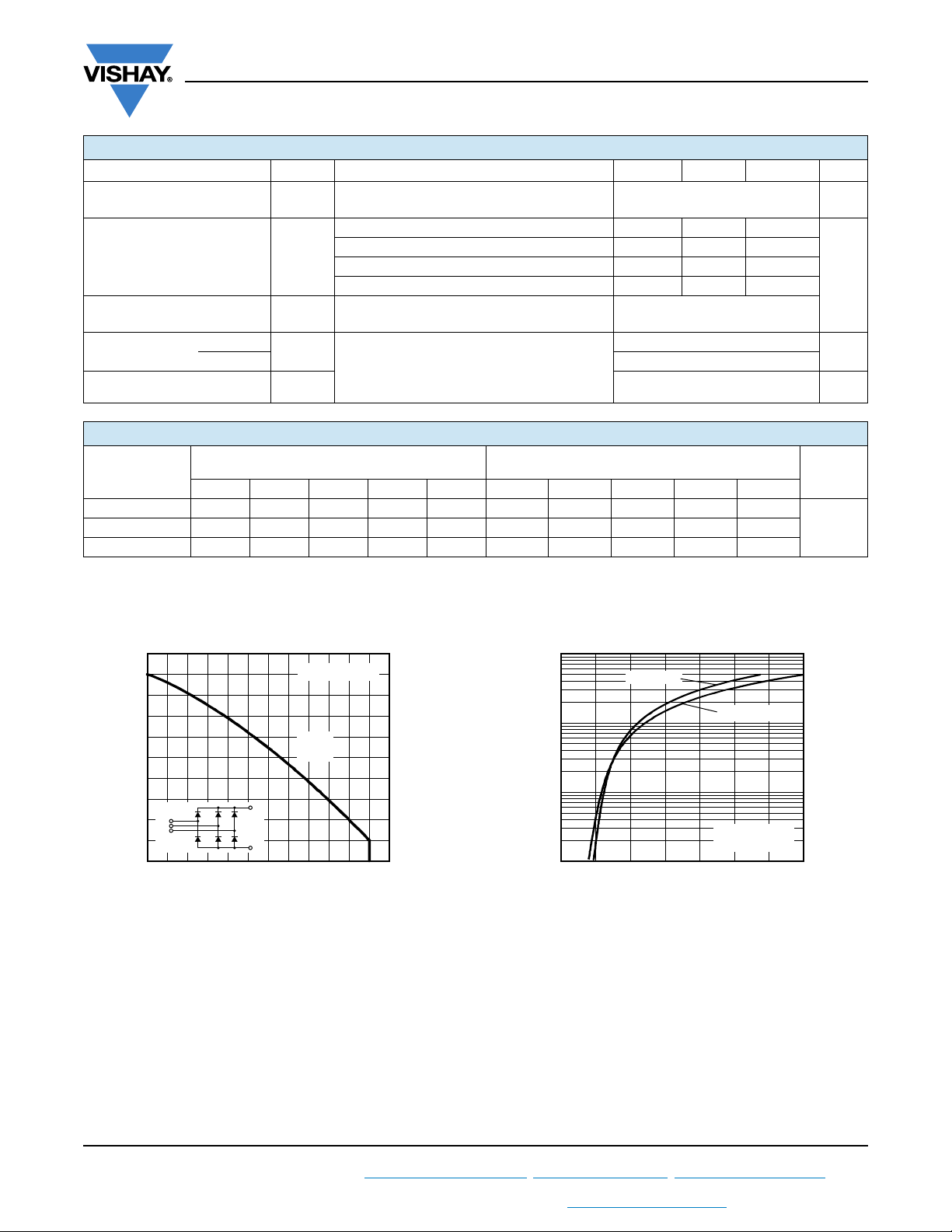
Fig. 1 - Current Ratings Characteristic Fig. 2 - Forward Voltage Drop Characteristics
5.MT..K Series
120°
(Rect.)
+
-
Total Output Current (A)
1000
TJ = 25 °C
100
10
Instantaneous On-State Current (A)
60
94353_02
1
0
21 3456
Instantaneous On-State Voltage (V)
TJ = 125 °C
5.MT..K Series
Per junction
7
Revision: 27-Feb-14
For technical questions within your region: DiodesAmericas@vishay.com
THIS DOCUMENT IS SUBJECT TO CHANGE WITHOUT NOTICE. THE PRODUCTS DESCRIBED HEREIN AND THIS DOCUMENT
ARE SUBJECT TO SPECIFIC DISCLAIMERS, SET FORTH AT www.vishay.com/doc?91000
3
, DiodesAsia@vishay.com, DiodesEurope@vishay.com
Document Number: 94353

Maximum Total Power Loss (W)
Total Output Current (A)
51510 25 353020 40 5045
55
0
94353_03a
80
60
180
220
0
20
140
100
120
200
40
160
120°
(Rect.)
5.MT..K Series
T
J
= 125 °C
VS-5.MT...KPbF, VS-9.MT...KPbF, VS-11.MT...KPbF Series
www.vishay.com
Vishay Semiconductors
350
300
250
200
On-State Current (A)
Peak Half Sine Wave
150
94353_04
Fig. 4 - Maximum Non-Repetitive Surge Current
At any rated load condition and with
rated V
5.MT..K Series
Per junction
1
applied following surge.
RRM
10
Number of Equal Amplitude Half
Cycle Current Pulses (N)
Fig. 3 - Total Power Loss Characteristics
= 125 °C
Initial T
J
at 60 Hz 0.0083 s
at 50 Hz 0.0100 s
100
220
200
180
160
140
120
100
80
60
40
20
Maximum Total Power Loss (W)
0
0
94353_03b
0.3 K/W
0.4 K/W
0.5 K/W
0.7 K/W
1.0 K/W
1.5 K/W
25 50 75 100
Maximum Allowable Ambient
Temperature (°C)
130
120
110
100
Temperature (°C)
90
Maximum Allowable Case
94353_06
~
80
20 40 60 80 1000
Total Output Current (A)
Fig. 6 - Current Ratings Characteristic
0.12 K/W
0.2 K/W
(Rect.)
+
-
R
thSA
= 0.05 K/W - ΔR
9.MT..K Series
120°
125
400
350
300
250
On-State Current (A)
Peak Half Sine Wave
200
5.MT..K Series
94353_05
Revision: 27-Feb-14
Per junction
150
0.01
Fig. 5 - Maximum Non-Repetitive Surge Current
For technical questions within your region: DiodesAmericas@vishay.com
THIS DOCUMENT IS SUBJECT TO CHANGE WITHOUT NOTICE. THE PRODUCTS DESCRIBED HEREIN AND THIS DOCUMENT
Maximum non-repetitive surge current
versus pulse train duration. Control
of conduction may not be maintained.
Initial TJ = 125 °C
No voltage reapplied
Rated V
0.1 1
Pulse Train Duration (s)
ARE SUBJECT TO SPECIFIC DISCLAIMERS, SET FORTH AT www.vishay.com/doc?91000
reapplied
RRM
Instantaneous On-State Current (A)
94353_07
4
1000
100
TJ = 25 °C
10
1
1.0 2.01.50.5 2.5 3.0 3.5
TJ = 125 °C
9.MT..K Series
Per junction
4.0
Total Output Current
Fig. 7 - Forward Voltage Drop Characteristics
Document Number: 94353
, DiodesAsia@vishay.com, DiodesEurope@vishay.com

VS-5.MT...KPbF, VS-9.MT...KPbF, VS-11.MT...KPbF Series
Maximum Total Power Loss (W)
Maximum Allowable Ambient
Temperature (°C)
25 50 75 100
125
0
R
thSA
= 0.05 K/W - ΔR
0.12 K/W
0.2 K/W
0.3 K/W
0.4 K/W
0.5 K/W
0.7 K/W
1.0 K/W
1.5 K/W
200
150
300
0
50
250
100
94353_08b
Peak Half Sine Wave
On-State Current (A)
Number of Equal Amplitude Half
Cycle Current Pulses (N)
10
100
1
At any rated load condition and with
rated V
RRM
applied following surge.
Initial TJ = 125 °C
at 60 Hz 0.0083 s
at 50 Hz 0.0100 s
94353_09
9.MT..K Series
Per junction
850
400
650
450
750
700
550
500
600
800
www.vishay.com
300
9.MT..K Series
T
= 125 °C
J
250
200
150
100
50
Maximum Total Power Loss (W)
0
0
10 20 30 40 50 7060
94353_08a
Total Output Current (A)
Vishay Semiconductors
120°
(Rect.)
9080
Fig. 8 - Total Power Loss Characteristics
Fig. 9 - Maximum Non-Repetitive Surge Current
1000
900
800
700
600
500
On-State Current (A)
Peak Half Sine Wave
9.MT..K Series
400
Per junction
300
0.01
94353_10
Revision: 27-Feb-14
Fig. 10 - Maximum Non-Repetitive Surge Current
For technical questions within your region: DiodesAmericas@vishay.com
THIS DOCUMENT IS SUBJECT TO CHANGE WITHOUT NOTICE. THE PRODUCTS DESCRIBED HEREIN AND THIS DOCUMENT
Maximum non-repetitive surge current
versus pulse train duration. Control
of conduction may not be maintained.
Pulse Train Duration (s)
Initial TJ = 125 °C
No voltage reapplied
Rated V
RRM
0.1
ARE SUBJECT TO SPECIFIC DISCLAIMERS, SET FORTH AT www.vishay.com/doc?91000
reapplied
130
120
110
100
Temperature (°C)
90
Maximum Allowable Case
80
0
94353_11
~
20 40 60 80 100
Total Output Current (A)
11.MT..K Series
120°
(Rect.)
+
-
120
Fig. 11 - Current Ratings Characteristic
1000
100
TJ = 25 °C
10
Instantaneous On-State Current (A)
1
1
94353_12
1.0 1.50.5 2.0 2.5 3.0 3.5
Instantaneous On-State Voltage (V)
TJ = 125 °C
11.MT..K Series
Per junction
4.0
Fig. 12 - Forward Voltage Drop Characteristics
5
Document Number: 94353
, DiodesAsia@vishay.com, DiodesEurope@vishay.com

VS-5.MT...KPbF, VS-9.MT...KPbF, VS-11.MT...KPbF Series
Maximum Total Power Loss (W)
Maximum Allowable Ambient
Temperature (°C)
25 50 75 100
125
0
R
thSA
= 0.058 K/W - ΔR
0.12 K/W
0.2 K/W
0.3 K/W
0.4 K/W
0.5 K/W
0.7 K/W
1.0 K/W
1.5 K/W
200
150
350
0
50
250
300
100
94353_13b
Peak Half Sine Wave
On-State Current (A)
Number of Equal Amplitude Half
Cycle Current Pulses (N)
10 1001
At any rated load condition and with
rated V
RRM
applied following surge.
94353_14
11.MT..K Series
Per junction
1000
400
700
500
800
600
900
Initial TJ = 125 °C
at 60 Hz 0.0083 s
at 50 Hz 0.0100 s
0.001
0.01
0.1
1
10
0.001
94353_16
0.01 0.1 1
Square Wave Pulse Duration (s)
Z
thJC
- Transient Thermal
Impedance (K/W)
10
Per junction
5.MT..K Series
11.MT..K Series
9.MT..K Series
Steady state value
R
thJC
= 1.07 K/W
R
thJC
= 0.86 K/W
R
thJC
= 0.70 K/W
(DC operation)
www.vishay.com
350
11.MT..K Series
= 125 °C
T
300
J
250
200
150
100
50
Maximum Total Power Loss (W)
0
94353_13a
2010 4030 6050 8070 10090
0
Total Output Current
Vishay Semiconductors
120°
(Rect.)
110
Fig. 13 - Total Power Loss Characteristics
1200
1100
1000
900
800
700
600
On-State Current (A)
Peak Half Sine Wave
500
400
0.01 0.1 1.0
94353_15
Maximum non-repetitive surge current
versus pulse train duration. Control
of conduction may not be maintained.
Initial TJ = 125 °C
No voltage reapplied
Rated V
11.MT..K Series
Per junction
Pulse Train Duration (s)
reapplied
RRM
Fig. 14 - Maximum Non-Repetitive Surge Current Fig. 15 - Maximum Non-Repetitive Surge Current
Revision: 27-Feb-14
For technical questions within your region: DiodesAmericas@vishay.com
THIS DOCUMENT IS SUBJECT TO CHANGE WITHOUT NOTICE. THE PRODUCTS DESCRIBED HEREIN AND THIS DOCUMENT
Fig. 16 - Thermal Impedance Z
6
Characteristics
thJC
, DiodesAsia@vishay.com, DiodesEurope@vishay.com
ARE SUBJECT TO SPECIFIC DISCLAIMERS, SET FORTH AT www.vishay.com/doc?91000
Document Number: 94353

Device code
621 43 7
11VS- 3 MT 160 K S90 PbF
5
2
4
7
- Current rating code:
5 = 55 A (average)
9 = 90 A (average)
11 = 110 A (average)
3
- Circuit configuration code:
1 = Negative half-controlled bridge
2 = Positive half-controlled bridge
3 = Full-controlled bridge
- Essential part number
1
- Vishay Semiconductors product
5
- Voltage code x 10 = V
RRM
(see Voltage Ratings table)
- PbF = Lead (Pb)-free
6
- Critical dV/dt:
None = 500 V/µs (standard value)
S90 = 1000 V/µs (special selection)
Full-controlled bridge
(5.MT...K, 9.MT...K, 11.MT..K)
A
D
1
B
EF
C
25
64 3
Positive half-controlled bridge
(5.MT...K, 9.MT...K, 11.MT..K)
AB C
D
EF
125
Negative half-controlled bridge
(5.MT...K, 9.MT...K, 11.MT..K)
64 3
A
DE F
BC
VS-5.MT...KPbF, VS-9.MT...KPbF, VS-11.MT...KPbF Series
www.vishay.com
Vishay Semiconductors
10
Rectangular gate pulse
a) Recommended load line for
rated dI/dt: 20 V, 30 Ω;
= 0.5 μs, tp ≥ 6 μs
t
r
b) Recommended load line for
1
≤ 30 % rated dI/dt: 20 V, 65 Ω
= 1 μs, tp ≥ 6 μs
t
r
0.1
V
GD
Instantaneous Gate Voltage (V)
0.01
0.001 0.01 0.1 1
94353_17
I
GD
5.MT...K, 9.MT...K, 11.MT...K Series
ORDERING INFORMATION TABLE
(a)
T
(b)
J
= -40 °C
T
J
T
= 25 °C
J
= 125 °C
Instantaneous Gate Current (A)
Fig. 17 - Gate Characteristics
(1) PGM = 100 W, tp = 500 μs
= 50 W, tp = 1 ms
(2) P
GM
= 20 W, tp = 25 ms
(3) P
GM
= 10 W, tp = 5 ms
(4) P
GM
(4)
Frequency Limited by P
(2)
(3)
(1)
G(AV)
1000 100 10
Note
• To order the optional hardware go to www.vishay.com/doc?95172
CIRCUIT CONFIGURATION
Dimensions www.vishay.com/doc?95004
Revision: 27-Feb-14
For technical questions within your region: DiodesAmericas@vishay.com
THIS DOCUMENT IS SUBJECT TO CHANGE WITHOUT NOTICE. THE PRODUCTS DESCRIBED HEREIN AND THIS DOCUMENT
ARE SUBJECT TO SPECIFIC DISCLAIMERS, SET FORTH AT www.vishay.com/doc?91000
LINKS TO RELATED DOCUMENTS
7
, DiodesAsia@vishay.com, DiodesEurope@vishay.com
Document Number: 94353

24 ± 0.5
(0.94 ± 0.02)
38 ± 0.5
(1.5 ± 0.02)
30 ± 0.5
(1.17 ± 0.02)
35 ± 0.3
(1.38 ± 0.01)
8.5 ± 0.5
(0.34 ± 0.02)
Fast-on tab 2.8 x 0.8 (type 110)
Screws M5 x 0.8 length 10
28 ± 1
(1.11 ± 0.04)
25.5 ± 0.5
(1.004 ± 0.02)
5 ± 0.3
(0.2 ± 0.01)
75 ± 0.5
(2.95 ± 0.02)
46 ± 0.3
(1.81 ± 0.01)
80 ± 0.3
(3.15 ± 0.01)
94 ± 0.3
(3.7 ± 0.01)
Ø 6.5 ± 0.2
(Ø 0.26 ± 0.01)
14 ± 0.3
(0.55 ± 0.01)
18 ± 0.3
(0.71 ± 0.01)
1
2
3
4
5
6
7
8
A
B
C
F
E
D
MTK (with and without optional barrier)
DIMENSIONS WITH OPTIONAL BARRIERS in millimeters (inches)
Outline Dimensions
Vishay Semiconductors
Document Number: 95004 For technical questions, contact: indmodules@vishay.com
Revision: 27-Aug-07 1
www.vishay.com

Outline Dimensions
Vishay Semiconductors
MTK (with and without optional barrier)
DIMENSIONS WITHOUT OPTIONAL BARRIERS in millimeters (inches)
Screws M5 x 0.8 length 10
28 ± 1
25.5 ± 0.5
(1.11 ± 0.04)
(1.004 ± 0.02)
5 ± 0.3
(0.2 ± 0.01)
75 ± 0.5
(2.95 ± 0.02)
Fast-on tab 2.8 x 0.8 (type 110)
30 ± 0.5
(1.17 ± 0.02)
24 ± 0.5
(0.94 ± 0.02)
35 ± 0.3
(1.38 ± 0.01)
8.5 ± 0.5
(0.34 ± 0.02)
1
3
Ø 6.5 ± 0.2
(Ø 0.26 ± 0.01)
A
2
4
D
B
E
46 ± 0.3
(1.81 ± 0.01)
80 ± 0.3
(3.15 ± 0.01)
94 ± 0.3
(3.7 ± 0.01)
C
F
5
7
6
14 ± 0.3
18 ± 0.3
(0.55 ± 0.01)
(0.71 ± 0.01)
8
www.vishay.com For technical questions, contact: indmodules@vishay.com
Document Number: 95004
2 Revision: 27-Aug-07

Legal Disclaimer Notice
www.vishay.com
Vishay
Disclaimer
ALL PRODUCT, PRODUCT SPECIFICATIONS AND DATA ARE SUBJECT TO CHANGE WITHOUT NOTICE TO IMPROVE
RELIABILITY, FUNCTION OR DESIGN OR OTHERWISE.
Vishay Intertechnology, Inc., its affiliates, agents, and employees, and all persons acting on its or their behalf (collectively,
“Vishay”), disclaim any and all liability for any errors, inaccuracies or incompleteness contained in any datasheet or in any other
disclosure relating to any product.
Vishay makes no warranty, representation or guarantee regarding the suitability of the products for any particular purpose or
the continuing production of any product. To the maximum extent permitted by applicable law, Vishay disclaims (i) any and all
liability arising out of the application or use of any product, (ii) any and all liability, including without limitation special,
consequential or incidental damages, and (iii) any and all implied warranties, including warranties of fitness for particular
purpose, non-infringement and merchantability.
Statements regarding the suitability of products for certain types of applications are based on Vishay’s knowledge of typical
requirements that are often placed on Vishay products in generic applications. Such statements are not binding statements
about the suitability of products for a particular application. It is the customer’s responsibility to validate that a particular
product with the properties described in the product specification is suitable for use in a particular application. Parameters
provided in datasheets and/or specifications may vary in different applications and performance may vary over time. All
operating parameters, including typical parameters, must be validated for each customer application by the customer’s
technical experts. Product specifications do not expand or otherwise modify Vishay’s terms and conditions of purchase,
including but not limited to the warranty expressed therein.
Except as expressly indicated in writing, Vishay products are not designed for use in medical, life-saving, or life-sustaining
applications or for any other application in which the failure of the Vishay product could result in personal injury or death.
Customers using or selling Vishay products not expressly indicated for use in such applications do so at their own risk. Please
contact authorized Vishay personnel to obtain written terms and conditions regarding products designed for such applications.
No license, express or implied, by estoppel or otherwise, to any intellectual property rights is granted by this document or by
any conduct of Vishay. Product names and markings noted herein may be trademarks of their respective owners.
Material Category Policy
Vishay Intertechnology, Inc. hereby certifies that all its products that are identified as RoHS-Compliant fulfill the
definitions and restrictions defined under Directive 2011/65/EU of The European Parliament and of the Council
of June 8, 2011 on the restriction of the use of certain hazardous substances in electrical and electronic equipment
(EEE) - recast, unless otherwise specified as non-compliant.
Please note that some Vishay documentation may still make reference to RoHS Directive 2002/95/EC. We confirm that
all the products identified as being compliant to Directive 2002/95/EC conform to Directive 2011/65/EU.
Vishay Intertechnology, Inc. hereby certifies that all its products that are identified as Halogen-Free follow Halogen-Free
requirements as per JEDEC JS709A standards. Please note that some Vishay documentation may still make reference
to the IEC 61249-2-21 definition. We confirm that all the products identified as being compliant to IEC 61249-2-21
conform to JEDEC JS709A standards.
Revision: 02-Oct-12
1
Document Number: 91000
 Loading...