

VS-40MT160P.PbF, VS-70MT160P.PbF, VS-100MT160P.PbF
MT...PA MT...PB
www.vishay.com
Three Phase Bridge (Power Modules), 45 A to 100 A
PRODUCT SUMMARY
I
O
V
RRM
Package MT...PA, MT...PB
Circuit Three phase bridge
45 A to 100 A
1600 V
Vishay Semiconductors
FEATURES
•Low V
• Low profile package
• Direct mounting to heatsink
• Flat pin/round pin versions with PCB solderable
• Low junction to case thermal resistance
• 3500 V
• UL approved file E78996 vie
• Designed and qualified for industrial level
• Material categorization: for definitions of compliance
APPLICATIONS
• Power conversion machines
•Welding
•UPS
•SMPS
• Motor drives
• General purpose and heavy duty application
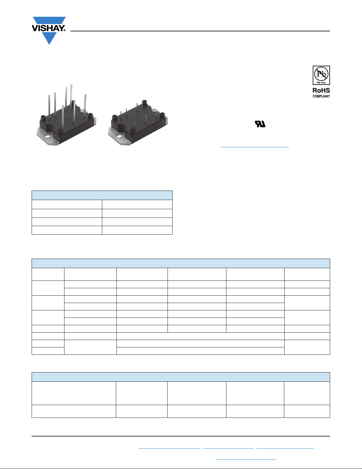
DESCRIPTION
A range of extremely compact three-phase rectifier bridges
offering efficient and reliable operation. The low profile
package has been specifically conceived to maximize space
saving and optimize the electrical layout of the application
specific power supplies.
F
terminals
insulation voltage
RMS
please see www.vishay.com/doc?99912
MAJOR RATINGS AND CHARACTERISTICS
SYMBOL CHARACTERISTICS
I
O
I
FSM
2
t
I
2
√t 3650 7240 10 130 A2√s
I
V
RRM
T
Stg
T
J
T
C
50 Hz 270 380 450
60 Hz 280 398 470
50 Hz 365 724 1013
60 Hz 325 660 920
Range
VALUES
40MT
45 75 100 A
100 80 80 °C
VALUES
70MT
1600 V
-40 to 125
-40 to 150
VALUES
100MT
ELECTRICAL SPECIFICATIONS
VOLTAGE RATINGS
V
, MAXIMUM
TYPE NUMBER
VS-40MT160P, VS-70MT160P,
VS-100MT160P
Revision: 16-Jul-14
For technical questions within your region: DiodesAmericas@vishay.com
THIS DOCUMENT IS SUBJECT TO CHANGE WITHOUT NOTICE. THE PRODUCTS DESCRIBED HEREIN AND THIS DOCUMENT
ARE SUBJECT TO SPECIFIC DISCLAIMERS, SET FORTH AT www.vishay.com/doc?91000
VOLTAGE CODE
REVERSE VOLTAGE
V
160 1600 1700 5
RRM
REPETITIVE PEAK
REVERSE VOLTAGE
V
1
, DiodesAsia@vishay.com, DiodesEurope@vishay.com
V
, MAXIMUM
RSM
NON-REPETITIVE PEAK
V
UNITS
A
A2s
°C
I
MAXIMUM AT
RRM
T
= 150 °C
J
mA
Document Number: 94538
VS-40MT160P.PbF, VS-70MT160P.PbF, VS-100MT160P.PbF
www.vishay.com
FORWARD CONDUCTION
PARAMETER SYMBOL TEST CONDITIONS
Maximum DC output
current at case
temperature
Maximum peak, one cycle
forward, non-repetitive on
state surge current
2
Maximum I
Maximum I
t for fusing I2t
2
√t for fusing I2√t t = 0.1 ms to 10 ms, no voltage reapplied 3650 7240 10 130 A2√s
Value of threshold voltage V
Slope resistance r
Maximum forward voltage
drop
I
I
FSM
F(TO)
V
120° rect. to conduction angle
O
t = 10 ms
t = 8.3 ms 280 398 470
t = 10 ms
t = 8.3 ms 240 335 400
t = 10 ms
t = 8.3 ms 325 660 920
t = 10 ms
t = 8.3 ms 240 467 665
No voltage
reapplied
100 % V
reapplied
RRM
No voltage
reapplied
100 % V
reapplied
RRM
Initial
T
= TJ maximum
J
TJ maximum
t
TJ = 25 °C; tp = 400 μs single junction
FM
(40MT, I
= 40 A ) (70M T, Ipk = 70 A) (100MT, Ipk = 100 A)
pk
Vishay Semiconductors
VALUES
40MT
0.78 0.82 0.75 V
14.8 9.5 8.1 mΩ
1.45 1.45 1.51 V
VALUES
70MT
VALUES
100MT
UNITS
45 75 100 A
100 80 80 °C
270 380 450
225 320 380
365 724 1013
253 512 600
A2s
Α
INSULATION TABLE
PARAMETER SYMBOL TEST CONDITIONS 40MT 70MT 100MT UNITS
RMS insulation voltage V
INS
TJ = 25 °C, all terminal shorted, f = 50 Hz, t = 1 s 3500 V
THERMAL AND MECHANICAL SPECIFICATIONS
PARAMETER SYMBOL TEST CONDITIONS 40MT 70MT 100MT UNITS
Maximum junction operating
temperature range
Maximum storage
temperature range
T
J
T
Stg
- 40 to 150
°C
- 40 to 125
DC operation per module 0.27 0.23 0.19
Maximum thermal resistance,
junction to case
Maximum thermal resistance,case to
heatsink per module
R
R
thJC
thCS
Mounting torque to heatsink
± 10 %
Approximate weight 65 g
DC operation per junction 1.6 1.38 1.14
120° rect. condunction angle per module 0.38 0.29 0.22
120° rect. condunction angle per junction 2.25 1.76 1.29
Mounting surface smooth, flat and greased
Heatsink compound thermal conduct i v i t y
0.1
= 0.42 W/mK
A mounting compound is recommended
and the torque should be rechecked after a
4Nm
period of 3 hours to allow for the spread of
the compound. Lubricated threads
K/W
CLEARANCE AND CREEPAGE DISTANCES
PARAMETER TEST CONDITIONS MT...PA MT...PB UNITS
Clearance
Creepage distance
External shortest distances in air between terminals
which are not internally short circuited together
Shortest distance along external surface of the insulating material
between terminals which are not internally short circuited together
10.9 12.3 mm
Revision: 16-Jul-14
For technical questions within your region: DiodesAmericas@vishay.com
THIS DOCUMENT IS SUBJECT TO CHANGE WITHOUT NOTICE. THE PRODUCTS DESCRIBED HEREIN AND THIS DOCUMENT
ARE SUBJECT TO SPECIFIC DISCLAIMERS, SET FORTH AT www.vishay.com/doc?91000
2
, DiodesAsia@vishay.com, DiodesEurope@vishay.com
Document Number: 94538
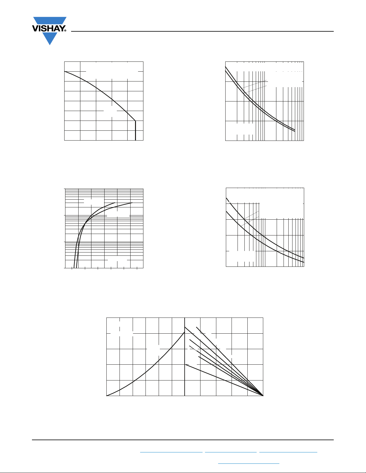
Total Output Current (A)
Maximum Allowable Case Temperature (°C)
80
90
100
110
120
130
140
150
160
0 1020304050
120˚
(Rect)
40MT...P
R (DC) = 0.27 K/W
Per Module
thJC
Instantaneous On-state Current (A)
Instantaneous On-state Voltage (V)
1
10
100
1000
0123456
Tj = 150˚C
Tj = 25˚C
40MT...P
Maximum Allowable Ambient Temperature (°C)Total Output Current (A)
Maximum Total Power Loss (W)
30 60 90 120 150
RthSA = 0.1 K/W - Delta R
0.3 K/W
0.4 K/W
0.5 K/W
1 K/W
0.2 K/W
0
50
100
150
200
250
0 102030405060
120˚
(Rect)
Tj = 150˚C
40MT...P
VS-40MT160P.PbF, VS-70MT160P.PbF, VS-100MT160P.PbF
www.vishay.com
250
200
150
100
Peak Half Sine Wave On-state Current (A)
50
110100
Number Of Equal Amplitude Half Cycle Current Pulses (N)
Vishay Semiconductors
At Any Rated Load Condition And With
Rated Vrrm Applied Following Surge.
40MT...P
Per Junction
Initial Tj = 150˚C
@ 60 Hz 0.0083 s
@ 50 Hz 0.0100 s
Fig. 1 - Current Rating Characteristics
Fig. 2 - On-State Voltage Drop Chracteristics
Fig. 3 - Maximum Non-Repetitive Surge Current
300
Maximum Non Repetitive Surge Current
Versus Pulse Train Duration. Control
Of Conduction May Not Be Maintained.
250
200
Initial T j = 150˚C
No Voltage Reapplied
Rated V rrm Reapplied
150
100
40MT...P
Per Junction
Peak Half Sine Wave On-state Current (A)
50
0.01 0.1 1
Pulse Train Duration(s)
Fig. 4 - Maximum Non-Repetitive Surge Current
Revision: 16-Jul-14
For technical questions within your region: DiodesAmericas@vishay.com
THIS DOCUMENT IS SUBJECT TO CHANGE WITHOUT NOTICE. THE PRODUCTS DESCRIBED HEREIN AND THIS DOCUMENT
0
Fig. 5 - Current Rating Nomogram (1 Module Per Heatsink)
3
, DiodesAsia@vishay.com, DiodesEurope@vishay.com
ARE SUBJECT TO SPECIFIC DISCLAIMERS, SET FORTH AT www.vishay.com/doc?91000
Document Number: 94538

Total Output Current (A)
Maximum Allowable Case Temperature (°C)
60
70
80
90
100
110
120
130
140
150
160
0 1020304050607080
120˚
(Rect)
70MT...P
R (DC) = 0.23 K/W
Per Module
thJC
Instantaneous On-state Current (A)
Instantaneous On-state Voltage (V)
1
10
100
1000
012345
Tj = 150˚C
Tj = 25˚C
70MT...P
Pulse Train Duration(s)
Peak Half Sine Wave On-state Current (A)
50
100
150
200
250
300
350
400
0.01 0.1 1
Maximum Non Repetitive Surge Current
Versus Pulse Train Duration. Control
Of Conduction May Not Be Maintained.
Initial T j = 150˚C
No Voltage Reapplied
Rated V rrm Reapplied
70MT...P
Per Junction
VS-40MT160P.PbF, VS-70MT160P.PbF, VS-100MT160P.PbF
www.vishay.com
350
300
250
200
150
Peak Half Sine Wave On-state Current (A)
100
110100
Number Of Equal Amplitude Half Cycle Current Pulses (N)
Vishay Semiconductors
At Any Rated Load Condition And With
Rated Vrrm Applied Following Surge.
70MT...P
Per Junction
Initial Tj = 150˚C
@ 60 Hz 0.0083 s
@ 50 Hz 0.0100 s
Fig. 6 - Current Rating Characteristics
Fig. 7 - On-State Voltage Drop Characteristics
Revision: 16-Jul-14
For technical questions within your region: DiodesAmericas@vishay.com
THIS DOCUMENT IS SUBJECT TO CHANGE WITHOUT NOTICE. THE PRODUCTS DESCRIBED HEREIN AND THIS DOCUMENT
Fig. 8 - Maximum Non-Repetitive Surge Current
Fig. 9 - Maximum Non-Repetitive Surge Current
300
250
200
150
70MT...P
Tj = 150˚C
120˚
(Rect)
RthSA = 0.1 K/W - Delta R
0.2 K/W
0.3 K/W
0.4 K/W
0.5 K/W
1 K/W
100
50
Maximum Total Power Loss (W)
0
020406080
Total Output Current (A)
0306090120150
Maximum Allowable Ambient Temperature (°C)
Fig. 10 - Current Rating Nomogram (1 Module Per Heatsink)
4
, DiodesAsia@vishay.com, DiodesEurope@vishay.com
ARE SUBJECT TO SPECIFIC DISCLAIMERS, SET FORTH AT www.vishay.com/doc?91000
Document Number: 94538

Total Output Current (A)
Maximum Allowable Case Temperature (°C)
40
60
80
100
120
140
40 50 60 70 80 90 100 110 120 130
120˚
(Rect)
Per Module
100MT...P
R (DC) = 0.19 K/W
thJC
Number Of Equal Amplitude Half Cycle Current Pulses (N)
Peak Half Sine Wave On-state Current (A)
100
150
200
250
300
350
400
110100
At Any Rated Load Condition And With
Rated Vrrm Applied Following Surge.
Initial Tj = 125˚C
@ 60 Hz 0.0083 s
@ 50 Hz 0.0100 s
100MT...P
Per Junction
Maximum Allowable Ambient Temperature (°C)Total Output Current (A)
Maximum Total Power Loss (W)
30 60 90 120 150
0.05 K/W
RthSA = 0.025 K/W - Delta R
0.5 K/W
1 K/
W
0.3 K/W
0.2 K/W
0.1 K/W
0
100
200
300
400
500
020406080100
120˚
(Rect)
Tj = 150˚C
100MT...P
VS-40MT160P.PbF, VS-70MT160P.PbF, VS-100MT160P.PbF
www.vishay.com
Vishay Semiconductors
Fig. 11 - Current Rating Characteristics
1000
100MT...P
100
10
Tj = 150˚C
Instantaneous On-state Current (A)
Tj = 25˚C
1
0.5 1 1.5 2 2.5 3 3.5 4
Instantaneous On-state Voltage (V)
Fig. 12 - On-State Voltage Drop Characteristics
Fig. 13 - Maximum Non-Repetitive Surge Current
500
Maximum Non Repetitive Surge Current
Versus Pulse Train Duration. Control
450
Of Conduction May Not Be Maintained.
400
350
300
Initial T j = 125˚C
No Voltage Reapplied
Rated V rrm Reapplied
250
200
150
100
100MT...P
Per Junction
50
Peak Half Sine Wave On-state Current (A)
0
0.01 0.1 1 10
Pulse Train Duration(s)
Fig. 14 - Maximum Non-Repetitive Surge Current
Revision: 16-Jul-14
For technical questions within your region: DiodesAmericas@vishay.com
THIS DOCUMENT IS SUBJECT TO CHANGE WITHOUT NOTICE. THE PRODUCTS DESCRIBED HEREIN AND THIS DOCUMENT
ARE SUBJECT TO SPECIFIC DISCLAIMERS, SET FORTH AT www.vishay.com/doc?91000
0
Fig. 15 - Current Rating Nomogram (1 Module Per Heatsink)
5
, DiodesAsia@vishay.com, DiodesEurope@vishay.com
Document Number: 94538

Square Wave Pulse Duration (s)
Transient Thermal Impedance Z
thJC
(K/W)
0.01
0.1
1
10
0.0001 0.001 0.01 0.1 1 10
Steady State Value
RthJC per junction =
1.6 K/W (40MT...P)
1.38 K/W (70MT...P
1.14 K/W (100MT...P)
DC Operation)
40MT...P
70MT...P
100MT...P
VS-40MT160P.PbF, VS-70MT160P.PbF, VS-100MT160P.PbF
www.vishay.com
Vishay Semiconductors
Fig. 16 - Thermal Impedance Z
ORDERING INFORMATION TABLE
Device code
VS-
1
1
2
3 - Circuit configuration code: 0 = 3-Phase rectifier bridge
4 - Essential part number
5 - Voltage code x 10 = V
6 - Pinout code
7
Characteristics
thJC
10 0 MT 160 P B PbF
43 5 7
- Vishay Semiconductors product
- Current rating code
10 = 100 A
(see Voltage Ratings table)
RRM
A = Flat pins
B = Round pins
- Lead (Pb)-free
4 = 45 A
7 = 75 A
62
CIRCUIT CONFIGURATION
Dimensions www.vishay.com/doc?95244
Revision: 16-Jul-14
For technical questions within your region: DiodesAmericas@vishay.com
THIS DOCUMENT IS SUBJECT TO CHANGE WITHOUT NOTICE. THE PRODUCTS DESCRIBED HEREIN AND THIS DOCUMENT
ARE SUBJECT TO SPECIFIC DISCLAIMERS, SET FORTH AT www.vishay.com/doc?91000
LINKS TO RELATED DOCUMENTS
6
, DiodesAsia@vishay.com, DiodesEurope@vishay.com
Document Number: 94538

4
2.5
42 ± 0.1
7
14
2
44.5
7
7
7
7
7.4
Ø 5.2 (x 2)
4
3
2
1
5
7
1.3
14
14
39.5
48.7
63.5 ± 0.25
32.5 ± 0.5
27.5
22
22
0.5
5.5
Ø 5
16
12 ± 0.5
10.5
5.5
0.5
Electrical
circuit
3, 4
5
6
7
1, 2
6
12
MTP Flat and Round Pin
DIMENSIONS FOR MTP WITH FLAT PIN in millimeters
Outline Dimensions
Vishay Semiconductors
Document Number: 95244 For technical questions, contact: indmodules@vishay.com
Revision: 07-Nov-07 1
www.vishay.com

Outline Dimensions
44.5
32.5 ± 0.1
27.5
22
1.3
14
14
39.5
48.7
63.5 ± 0.25
Electrical
circuit
3, 4
5
6
7
1, 2
7
7
7
7
4
3
2
1
5
7
Ø 5.2 (x 2)
7.4
10.5
4
Ø 5
Ø 1.1
12 ± 0.5
16
31.8
12
2.5
4
Ø 5
14
7
7
6
20.5 ± 0.1
Vishay Semiconductors
MTP Flat and Round Pin
DIMENSIONS FOR MTP WITH ROUND PIN in millimeters
www.vishay.com For technical questions, contact: indmodules@vishay.com
2 Revision: 07-Nov-07
Document Number: 95244

Legal Disclaimer Notice
www.vishay.com
Vishay
Disclaimer
ALL PRODUCT, PRODUCT SPECIFICATIONS AND DATA ARE SUBJECT TO CHANGE WITHOUT NOTICE TO IMPROVE
RELIABILITY, FUNCTION OR DESIGN OR OTHERWISE.
Vishay Intertechnology, Inc., its affiliates, agents, and employees, and all persons acting on its or their behalf (collectively,
“Vishay”), disclaim any and all liability for any errors, inaccuracies or incompleteness contained in any datasheet or in any other
disclosure relating to any product.
Vishay makes no warranty, representation or guarantee regarding the suitability of the products for any particular purpose or
the continuing production of any product. To the maximum extent permitted by applicable law, Vishay disclaims (i) any and all
liability arising out of the application or use of any product, (ii) any and all liability, including without limitation special,
consequential or incidental damages, and (iii) any and all implied warranties, including warranties of fitness for particular
purpose, non-infringement and merchantability.
Statements regarding the suitability of products for certain types of applications are based on Vishay’s knowledge of typical
requirements that are often placed on Vishay products in generic applications. Such statements are not binding statements
about the suitability of products for a particular application. It is the customer’s responsibility to validate that a particular
product with the properties described in the product specification is suitable for use in a particular application. Parameters
provided in datasheets and/or specifications may vary in different applications and performance may vary over time. All
operating parameters, including typical parameters, must be validated for each customer application by the customer’s
technical experts. Product specifications do not expand or otherwise modify Vishay’s terms and conditions of purchase,
including but not limited to the warranty expressed therein.
Except as expressly indicated in writing, Vishay products are not designed for use in medical, life-saving, or life-sustaining
applications or for any other application in which the failure of the Vishay product could result in personal injury or death.
Customers using or selling Vishay products not expressly indicated for use in such applications do so at their own risk. Please
contact authorized Vishay personnel to obtain written terms and conditions regarding products designed for such applications.
No license, express or implied, by estoppel or otherwise, to any intellectual property rights is granted by this document or by
any conduct of Vishay. Product names and markings noted herein may be trademarks of their respective owners.
Material Category Policy
Vishay Intertechnology, Inc. hereby certifies that all its products that are identified as RoHS-Compliant fulfill the
definitions and restrictions defined under Directive 2011/65/EU of The European Parliament and of the Council
of June 8, 2011 on the restriction of the use of certain hazardous substances in electrical and electronic equipment
(EEE) - recast, unless otherwise specified as non-compliant.
Please note that some Vishay documentation may still make reference to RoHS Directive 2002/95/EC. We confirm that
all the products identified as being compliant to Directive 2002/95/EC conform to Directive 2011/65/EU.
Vishay Intertechnology, Inc. hereby certifies that all its products that are identified as Halogen-Free follow Halogen-Free
requirements as per JEDEC JS709A standards. Please note that some Vishay documentation may still make reference
to the IEC 61249-2-21 definition. We confirm that all the products identified as being compliant to IEC 61249-2-21
conform to JEDEC JS709A standards.
Revision: 02-Oct-12
1
Document Number: 91000
 Loading...