Vishay VS-40MT120UHAPbF, VS-40MT120UHTAPbF Data Sheet

www.vishay.com
MTP
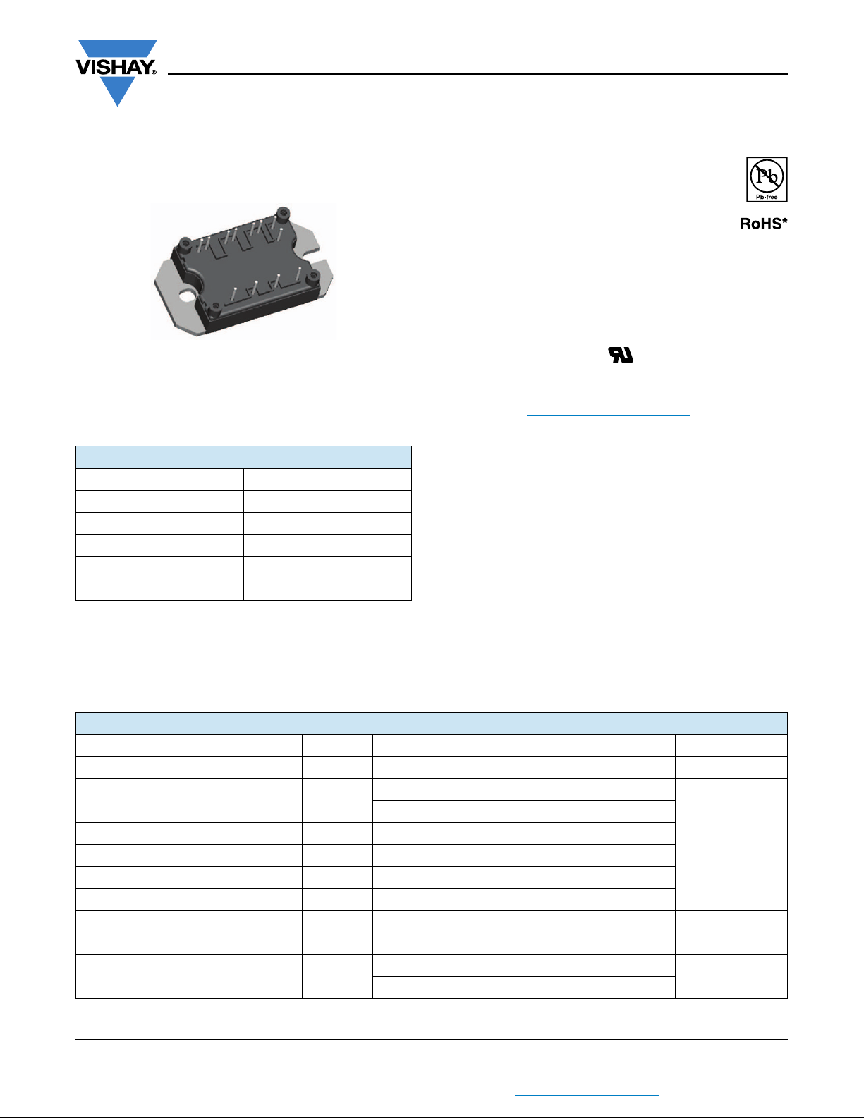
“Half Bridge” IGBT MTP (Ultrafast NPT IGBT), 80 A
PRODUCT SUMMARY
V
CES
typical at VGE = 15 V 3.36 V
V
CE(on)
at TC = 25 °C 80 A
I
C
Speed 8 kHz to 30 kHz
Package MTP
Circuit Half bridge
VS-40MT120UHAPbF, VS-40MT120UHTAPbF
Vishay Semiconductors
FEATURES
• Ultrafast Non Punch Through (NPT) technology
1200 V
•Positive V
• 10 μs short circuit capability
• Square RBSOA
•HEXFRED
recovery and low V
•Al2O3 DBC
• Optional SMD thermistor (NTC)
• Very low stray inductance design for high speed operation
• UL approved file E78996
• Designed and qualified for industrial level
• Material categorization: for definitions of compliance
please see www.vishay.com/doc?99912
Note
*
Thi s datasheet pro vi des information about parts that are
RoHS-compliant and / or parts that are non-RoHS-compliant. For
example, parts with lead (Pb) terminations are not RoHS-compliant.
Please see the information / tables in this datasheet for details.
BENEFITS
• Optimized for welding, UPS and SMPS applications
• Rugged with ultrafast performance
• Benchmark efficiency above 20 kHz
• Outstanding ZVS and hard switching operation
• Low EMI, requires less snubbing
• Excellent current sharing in parallel operation
• Direct mounting to heatsink
• PCB solderable terminals
• Very low junction to case thermal resistance
temperature coefficient
CE(on)
®
antiparallel diodes with ultrasoft reverse
F
Available
Available
ABSOLUTE MAXIMUM RATINGS
PARAMETER SYMBOL TEST CONDITIONS MAX. UNITS
Collector to emitter breakdown voltage V
Continuous collector current I
Pulsed collector current I
Clamped inductive load current I
Diode continuous forward current I
Diode maximum forward current I
Gate to emitter voltage V
RMS isolation voltage V
Maximum power dissipation (only IGBT) P
Revision: 18-Jun-15
For technical questions within your region: DiodesAmericas@vishay.com
THIS DOCUMENT IS SUBJECT TO CHANGE WITHOUT NOTICE. THE PRODUCTS DESCRIBED HEREIN AND THIS DOCUMENT
ARE SUBJECT TO SPECIFIC DISCLAIMERS, SET FORTH AT www.vishay.com/doc?91000
CES
C
CM
LM
F
FM
GE
ISOL
D
TC = 25 °C 80
= 104 °C 40
T
C
TC = 105 °C 21
Any terminal to case, t = 1 min 2500
TC = 25 °C 463
T
= 100 °C 185
C
1
, DiodesAsia@vishay.com, DiodesEurope@vishay.com
1200 V
160
160
160
± 20
Document Number: 94507
A
V
W

VS-40MT120UHAPbF, VS-40MT120UHTAPbF
www.vishay.com
ELECTRICAL SPECIFICATIONS (TJ = 25 °C unless otherwise specified)
PARAMETER SYMBOL TEST CONDITIONS MIN. TYP. MAX. UNITS
Collector to emitter
breakdown voltage
Temperature coefficient of
breakdown voltage
Collector to emitter saturation voltage V
Gate threshold voltage V
Temperature coefficient of
threshold voltage
Transconductance g
Zero gate voltage collector current I
Gate to emitter leakage current I
V
V
(BR)CES
(BR)CES
VGE = 0 V, IC = 250 μA 1200 - - V
/TJVGE = 0 V, IC = 3 mA (25 °C to 125 °C) - +1.1 - V/°C
VGE = 15 V, IC = 40 A - 3.36 3.59
= 15 V, IC = 80 A - 4.53 4.91
V
GE
= 15 V, IC = 40 A, TJ = 150 °C - 3.88 4.10
V
GE
= 15 V, IC = 80 A, TJ = 150 °C - 5.35 5.68
V
GE
VCE = VGE, IC = 500 μA 4 - 6
VCE = VGE, IC = 1 mA (25 °C to 125 °C) - -12 - mV/°C
J
VCE = 50 V, IC = 40 A, PW = 80 μs - 35 - S
VGE = 0 V, V
= 0 V, V
V
GE
V
= 0 V, V
GE
= 1200 V, TJ = 25 °C - - 250 μA
CE
= 1200 V, TJ = 125 °C - 0.4 1.0
CE
= 1200 V, TJ = 150 °C - 0.2 10
CE
VGE = ± 20 V - - ± 250 nA
V
CE(on)
GE(th)
GE(th)
/T
fe
CES
GES
Vishay Semiconductors
V
mA
SWITCHING CHARACTERISTICS (TJ = 25 °C unless otherwise specified)
PARAMETER SYMBOL TEST CONDITIONS MIN. TYP. MAX. UNITS
Total gate charge (turn-on) Q
Gate to collector charge (turn-on) Q
Turn-on switching loss E
Turn-off switching loss E
Total switching loss E
Turn-on switching loss E
Turn-off switching loss E
Total switching loss E
Input capacitance C
Reverse transfer capacitance C
g
ge
gc
on
off
tot
on
off
tot
ies
oes
res
Reverse bias safe operating area RBSOA
Short circuit safe operating area SCSOA
IC = 40 A
= 600 V
V
CC
V
= 15 V
GE
VCC = 600 V, IC = 40 A, VGE = 15 V,
R
= 5 , L = 200 μH, TJ = 25 °C,
g
energy losses include tail and diode
reverse recovery
VCC = 600 V, IC = 40 A, VGE = 15 V,
R
= 5 , L = 200 μH, TJ = 125 °C,
g
energy losses include tail and diode
reverse recovery
VGE = 0 V
V
= 30 V
CC
f = 1.0 MHz
= 150 °C, IC = 160 A
T
J
= 1000 V, Vp = 1200 V
V
CC
R
= 5 , VGE = + 15 V to 0 V
g
T
= 150 °C,
J
= 900 V, Vp = 1200 V
V
CC
R
= 5 , VGE = + 15 V to 0 V
g
- 399 599
-4365
nCGate to emitter charge (turn-on) Q
- 187 281
- 1.14 1.71
- 1.35 2.02
- 2.49 3.73
- 1.60 2.40
mJ
- 1.62 2.43
- 3.22 4.82
- 5521 8282
- 380 570
pFOutput capacitance C
- 171 257
Fullsquare
10 - - μs
Revision: 18-Jun-15
For technical questions within your region: DiodesAmericas@vishay.com
THIS DOCUMENT IS SUBJECT TO CHANGE WITHOUT NOTICE. THE PRODUCTS DESCRIBED HEREIN AND THIS DOCUMENT
ARE SUBJECT TO SPECIFIC DISCLAIMERS, SET FORTH AT www.vishay.com/doc?91000
2
, DiodesAsia@vishay.com, DiodesEurope@vishay.com
Document Number: 94507

VS-40MT120UHAPbF, VS-40MT120UHTAPbF
R
0
R
1
-------
1
T
0
------
1
T
1
------
–
exp=
www.vishay.com
DIODE SPECIFICATIONS (TJ = 25 °C unless otherwise specified)
PARAMETER SYMBOL TEST CONDITIONS MIN. TYP. MAX. UNITS
IC = 40 A - 2.98 3.38
= 80 A - 3.90 4.41
I
C
Diode forward voltage drop V
Reverse recovery energy of the diode E
Diode reverse recovery time t
Peak reverse recovery current I
FM
rec
rr
rr
= 40 A, TJ = 125 °C - 3.08 3.39
I
C
= 80 A, TJ = 125 °C - 4.29 4.72
I
C
= 40 A, TJ = 150 °C - 3.12 3.42
I
C
VGE = 15 V, Rg = 5 , L = 200 μH
V
= 600 V, IC = 40 A
CC
T
= 125 °C
J
THERMISTOR SPECIFICATIONS (40MT120UHTAPbF only)
PARAMETER SYMBOL TEST CONDITIONS MIN. TYP. MAX. UNITS
(1)
Resistance R
Sensitivity index of the
thermistor material
Notes
(1)
T0, T1 are thermistor´s temperatures
(2)
, temperature in Kelvin
0
(1)(2)
T0 = 25 °C - 30 - k
T0 = 25 °C
T
= 85 °C
1
Vishay Semiconductors
- 574 861 μJ
- 120 180 ns
-4365A
- 4000 - K
V
THERMAL AND MECHANICAL SPECIFICATIONS
PARAMETER SYMBOL TEST CONDITIONS MIN. TYP. MAX. UNITS
Operating junction temperature range T
Storage temperature range T
Junction to case
IGBT
Case to sink per module R
Clearance
Creepage
(1)
(2)
J
Stg
R
thJC
Heatsink compound thermal conductivity = 1 W/mK - 0.06 -
thCS
External shortest distance in air between 2 terminals 5.5 - -
Shortest distance along external surface of the
insulating material between 2 terminals
A mounting compound is recommended and the
Mounting torque to heatsink
torque should be checked after 3 hours to allow for
the spread of the compound. Lubricated threads.
Weight 66 g
-40 - 150
-40 - 125
- - 0.29
8--
3 ± 10 % Nm
°C
°C/WDiode - - 0.61
mm
Revision: 18-Jun-15
For technical questions within your region: DiodesAmericas@vishay.com
THIS DOCUMENT IS SUBJECT TO CHANGE WITHOUT NOTICE. THE PRODUCTS DESCRIBED HEREIN AND THIS DOCUMENT
ARE SUBJECT TO SPECIFIC DISCLAIMERS, SET FORTH AT www.vishay.com/doc?91000
3
, DiodesAsia@vishay.com, DiodesEurope@vishay.com
Document Number: 94507

www.vishay.com
0 20406080100120140160
TC(°C)
0
20
40
60
80
100
I
C
(
A
)
0 20406080100120140160
TC(°C)
0
100
200
300
400
500
600
P
D
(
W
)
10 100 1000 10 000
V
CE
(V)
1
10
100
1000
I
C
(
A
)
VS-40MT120UHAPbF, VS-40MT120UHTAPbF
Vishay Semiconductors
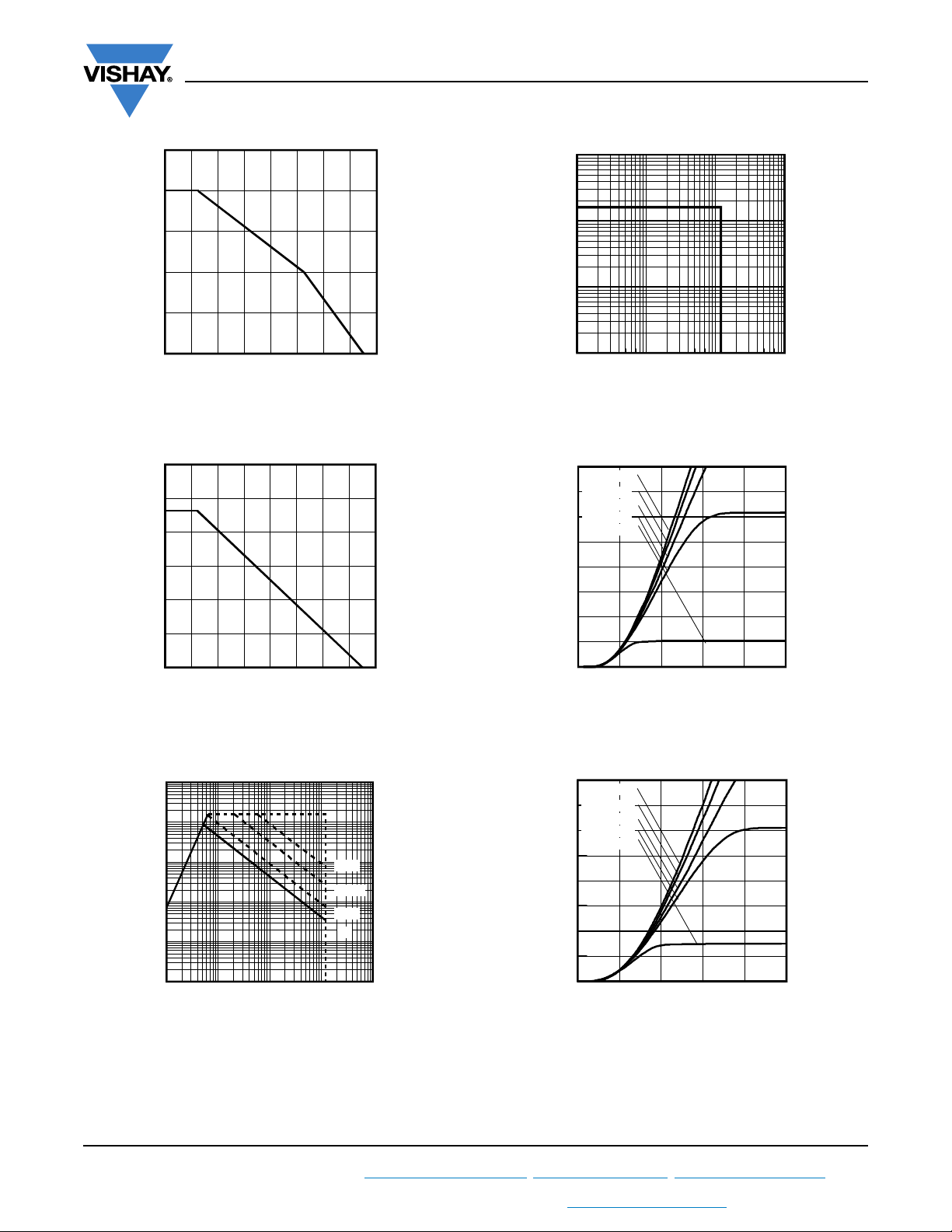
Fig. 1 - Maximum DC Collector Current vs. Case Temperature
Fig. 2 - Power Dissipation vs. Case Temperature
1000
100
10
)
A
(
C
I
1
0.1
0.01
1 10 100 1000 10000
Revision: 18-Jun-15
For technical questions within your region: DiodesAmericas@vishay.com
THIS DOCUMENT IS SUBJECT TO CHANGE WITHOUT NOTICE. THE PRODUCTS DESCRIBED HEREIN AND THIS DOCUMENT
Fig. 4 - Reverse BIAS SOA
= 150 °C; VGE = 15 V
T
J
160
VGE = 18V
140
VGE = 1 5V
VGE = 1 2V
120
VGE = 1 0V
VGE = 8.0V
100
)
A
(
80
E
C
I
60
40
20
0
0246810
V
CE
Fig. 5 - Typical IGBT Output Characteristics
T
= - 40 °C; tp = 80 μs
J
160
VGE = 18V
140
VGE = 15V
VGE = 12V
120
VGE = 10V
VGE = 8.0V
100
)
A
(
80
E
C
I
60
40
20
0
0246810
V
CE
Fig. 6 - Typical IGBT Output Characteristics
T
= 25 °C; tp = 80 μs
J
V
(V)
CE
Fig. 3 - Forward SOA
T
= 25 °C; TJ 150 °C
C
10 μs
100 μs
10ms
DC
4
, DiodesAsia@vishay.com, DiodesEurope@vishay.com
ARE SUBJECT TO SPECIFIC DISCLAIMERS, SET FORTH AT www.vishay.com/doc?91000
(V)
(V)
Document Number: 94507
 Loading...