

www.vishay.com
DO-203AB (DO-5)
(Stud Version), 40 A, 70 A, 85 A
PRODUCT SUMMARY
I
F(AV)
Package DO-203AB (DO-5)
Circuit configuration Single diode
40 A, 70 A, 85 A
VS-40HFL, VS-70HFL, VS-85HFL Series
Fast Recovery Diodes
FEATURES
• Short reverse recovery time
• Low stored charge
• Wide current range
• Excellent surge capabilities
• Stud cathode and stud anode versions
• Types up to 100 V
• Material categorization: For definitions of compliance
please see www.vishay.com/doc?99912
TYPICAL APPLICATIONS
• DC power supplies
•Inverters
• Converters
• Choppers
• Ultrasonic systems
• Freewheeling diodes
Vishay Semiconductors
RRM
MAJOR RATINGS AND CHARACTERISTICS
PARAMETER TEST CONDITIONS 40HFL 70HFL 85HFL UNITS
I
F(AV)
I
FSM
2
I
t
2
I
t 11 300 34 650 85 560 I2s
V
RRM
t
rr
T
J
T
maximum 85 85 85 °C
C
50 Hz 400 700 1100
60 Hz 420 730 1151
50 Hz 800 2450 6050
60 Hz 730 2240 5523
Range 100 to 1000 100 to 1000 100 to 1000 V
Characteristics table
Range -40 to 125 -40 to 125 -40 to 125 °C
40 70 85 A
See Recovery
See Recovery
Characteristics table
See Recovery
Characteristics table
A
A2s
ns
Revision: 22-Jan-14
For technical questions within your region: DiodesAmericas@vishay.com
THIS DOCUMENT IS SUBJECT TO CHANGE WITHOUT NOTICE. THE PRODUCTS DESCRIBED HEREIN AND THIS DOCUMENT
1
, DiodesAsia@vishay.com, DiodesEurope@vishay.com
ARE SUBJECT TO SPECIFIC DISCLAIMERS, SET FORTH AT www.vishay.com/doc?91000
Document Number: 93150

VS-40HFL, VS-70HFL, VS-85HFL Series
www.vishay.com
ELECTRICAL SPECIFICATIONS
VOLTAGE RATINGS
V
, MAXIMUM
RRM
TYPE NUMBER
(1)
PEAK REPETITIVE
REVERSE VOLTAGE
T
= - 40 °C TO 125 °C
J
V
VS-40HFL10S02, VS-40HFL10S05 100 150
VS-40HFL20S02, VS-40HFL20S05 200 300
VS-40HFL40S02, VS-40HFL40S05 400 500
VS-40HFL60S02, VS-40HFL60S05 600 700
VS-40HFL80S05 800 900
VS-40HFL100S05 1000 1100
VS-70HFL10S02, VS-70HFL10S05 100 150
VS-70HFL20S02, VS-70HFL20S05 200 300
VS-70HFL40S02, VS-70HFL40S05 400 500
VS-70HFL60S02, VS-70HFL60S05 600 700
VS-70HFL80S05 800 900
VS-70HFL100S05 1000 1100
VS-85HFL10S02, VS-85HFL10S05 100 150
VS-85HFL20S02, VS-85HFL20S05 200 300
VS-85HFL40S02, VS-85HFL40S05 400 500
VS-85HFL60S02, VS-85HFL60S05 600 700
VS-85HFL80S05 800 900
VS-85HFL100S05 1000 1100
Note
(1)
Types listed are cathode case, for anode case add “R” to code, i.e. 40HFLR20S02, 85HFLR100S05 etc.
V
, MAXIMUM PEAK
RSM
NON-REPETITIVE
REVERSE VOLTAGE
T
= 25 °C TO 125 °C
J
V
Vishay Semiconductors
I
, MAXIMUM PEAK REVERSE
FM
CURRENT AT RATED V
mA
= 25 °C TJ = 125 °C
T
J
0.1 10
0.1 15
0.1 20
RRM
FORWARD CONDUCTION
PARAMETER SYMBOL TEST CONDITIONS 40HFL 70HFL 85HFL UNITS
Maximum average forward current
at maximum case temperature
Maximum RMS forward current I
Maximum peak repetitive forward current I
Maximum peak, one-cycle
non-repetitive forward current
Maximum I
Maximum I
2
t for fusing I2t
2
t for fusing
(1)
Maximum value of threshold voltage V
Maximum value of forward slope resistance r
Maximum forward voltage drop V
Note
(1)I2
t for time tx = I2t x t
x
I
F(AV)
F(RMS)
FRM
I
FSM
180° conduction, half sine wave
Sinusoidal half wave, 30° conduction 220 380 470 A
t = 10 ms
t = 8.3 ms 420 730 1151
t = 10 ms
t = 8.3 ms 500 870 1369
t = 10 ms
t = 8.3 ms 730 2240 5523
t = 10 ms
t = 8.3 ms 1030 3160 7810
Sinusoidal half wave, 100
% V
reapplied,
RRM
initial T
= TJ maximum
J
Sinusoidal half wave,
no voltage reapplied,
initial T
= TJ maximum
J
100 % V
initial T
reapplied,
RRM
= TJ maximum
J
No voltage reapplied,
initial T
= TJ maximum
J
I2t t = 0.1 ms to 10 ms, no voltage reapplied 11 300 34 650 85 560 A2s
F(TO)
TJ = 125 °C
F
TJ = 25 °C, IFM = x I
FM
F(AV)
40 70 85 A
75 °C
63 110 134 A
400 700 1100
475 830 1308
800 2450 6050
1130 3460 8556
1.081 1.085 1.128 V
6.33 3.40 2.11 m
1.95 1.85 1.75 V
A
2
s
A
Revision: 22-Jan-14
For technical questions within your region: DiodesAmericas@vishay.com
THIS DOCUMENT IS SUBJECT TO CHANGE WITHOUT NOTICE. THE PRODUCTS DESCRIBED HEREIN AND THIS DOCUMENT
ARE SUBJECT TO SPECIFIC DISCLAIMERS, SET FORTH AT www.vishay.com/doc?91000
2
, DiodesAsia@vishay.com, DiodesEurope@vishay.com
Document Number: 93150
VS-40HFL, VS-70HFL, VS-85HFL Series
www.vishay.com
RECOVERY CHARACTERISTICS
PARAMETER SYMBOL TEST CONDITIONS
TJ = 25 °C, IF = 1 A to VR = 30 V,
dI
/dt = 100 A/μs
Typical reverse recovery time t
rr
F
= 25 °C, - dIF/dt = 25 A/μs,
T
J
I
= x rated I
FM
F(AV)
TJ = 25 °C, IF = 1 A to VR = 30 V,
dI
/dt = 100 A/μs
Typical reverse recovered charge Q
rr
F
= 25 °C, - dIF/dt = 25 A/μs,
T
J
I
= x rated I
FM
F(AV)
40HFL... 70HFL... 85HFL...
S02S05S02S05S02S05
70 180 60 150 50 120
200 500 200 500 200 500
160 750 90 500 70 340
240 1300 240 1300 240 1300
THERMAL AND MECHANICAL SPECIFICATIONS
PARAMETER SYMBOL TEST CONDITIONS 40HFL 70HFL 85HFL UNITS
Junction operating temperature range T
Storage temperature range T
Maximum thermal resistance,
junction to case
Maximum thermal resistance,
case to heatsink
Maximum allowable mounting torque
(+ 0 %, - 10 %)
Approximate weight
Case style JEDEC DO-203AB (DO-5)
Notes
(1)
Recommended for pass-through holes
(2)
Recommended for holed threaded heatsinks
R
R
J
Stg
thJC
thCS
DC operation 0.60 0.36 0.30
Mounting surface, smooth,
flat and greased
Not lubricated thread, tighting on nut
Lubricated thread, tighting on nut
(1)
Not lubricated thread, tighting on hexagon
Lubricated thread, tighting on hexagon
Vishay Semiconductors
- 40 to 125
- 40 to 150
0.25
(1)
(2)
(2)
3.4 (30)
2.3 (20)
4.2 (37)
3.2 (28)
25
0.88
UNITS
(lbf · in)
ns
nC
°C
K/W
N · m
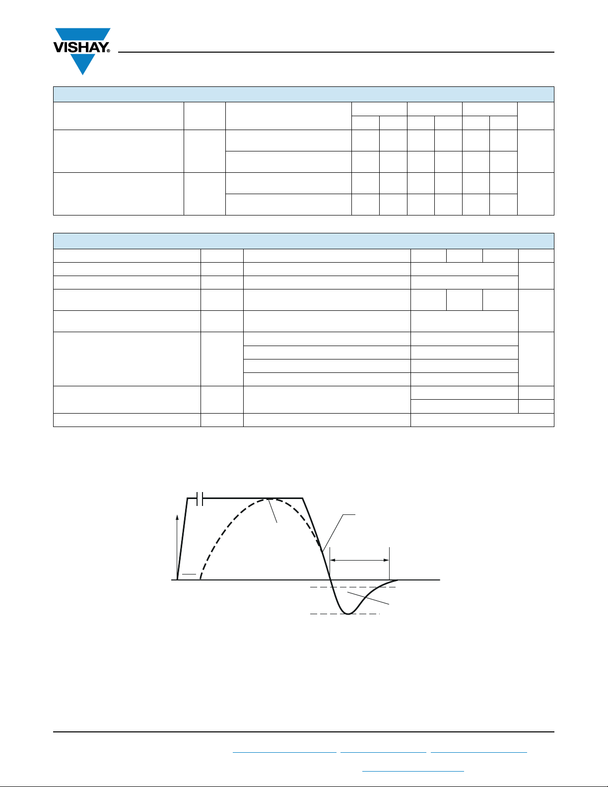
I
F
dI
F
I
t
t
IF, IFM - Peak forward current prior to commulation
/dt - Rate of fail forward current
-dI
F
(REC) - Peak reverse recovery current
I
RRM
- Reverse recovery time
t
rr
- Reverse recovered charge
Q
rr
FM
V
I
R
RRM (REC)
I
RRM (REC)
dt
t
rr
Q
rr
Fig. 1 - Reverse Recovery Time Test Waveform
Revision: 22-Jan-14
For technical questions within your region: DiodesAmericas@vishay.com
THIS DOCUMENT IS SUBJECT TO CHANGE WITHOUT NOTICE. THE PRODUCTS DESCRIBED HEREIN AND THIS DOCUMENT
ARE SUBJECT TO SPECIFIC DISCLAIMERS, SET FORTH AT www.vishay.com/doc?91000
3
, DiodesAsia@vishay.com, DiodesEurope@vishay.com
Document Number: 93150

www.vishay.com
Average Forward Current (A) Maximum Allowable Ambient Temperature (°C)
Maximum Average Forward Power Loss (W)
Ø = 180 °
120 °
90 °
60 °
30 °
0
15 205010 253035 304040 20 50 60 7010 9080 100
10
20
30
40
50
60
70
Ø
Conduction Angle
RMS limit
TJ = 125 °C
40HFL...
R
thSA
= 0.3 - ΔR K/W
0.5 - ΔR
0.7 - ΔR
1.0 - ΔR
1.5 - ΔR
2.0 - ΔR
3 - ΔR
4 - ΔR
5 - ΔR
RMS limit
TJ = 25 °C
40HFL...
R
thSA
= 0.3 - ΔR K/W
0.5 - ΔR
Ø = DC
180°
120°
60°
Conduction Angle
Ø
0.7 - ΔR
1.0 - ΔR
1.5 - ΔR
2.0- ΔR
3 - ΔR
4 - ΔR
30 4010020 5060 304070 20 50 60 7010 9080 100
0
10
20
30
40
50
60
100
90
80
70
Average Forward Current (A) Maximum Allowable Ambient Temperature (°C)
Maximum Average Forward Power Loss (W)
RMS limit
TJ = 125 °C
70HFL...
R
thSA
= 0.3 - ΔR K/W
0.5 - ΔR
Ø = 180°
120°
90°
60°
30°
Ø
Conduction Angle
0.7 - ΔR
1.0 - ΔR
1.5 - ΔR
2.0 - ΔR
3 - ΔR
4 -
ΔR
30 4010020 5060 304070 20 50 60 7010 9080 100
Average Forward Current (A) Maximum Allowable Ambient Temperature (°C)
0
20
40
60
100
120
80
Maximum Average Forward Power Loss (W)
Fig. 2 - Current Rating Nomogram (Sinusoidal Waveforms), 40HFL Series
VS-40HFL, VS-70HFL, VS-85HFL Series
Vishay Semiconductors
Revision: 22-Jan-14
Fig. 3 - Current Rating Nomogram (Rectangular Waveforms), 40HFL Series
For technical questions within your region: DiodesAmericas@vishay.com
THIS DOCUMENT IS SUBJECT TO CHANGE WITHOUT NOTICE. THE PRODUCTS DESCRIBED HEREIN AND THIS DOCUMENT
Fig. 4 - Current Rating Nomogram (Sinusoidal Waveforms), 70HFL Series
ARE SUBJECT TO SPECIFIC DISCLAIMERS, SET FORTH AT www.vishay.com/doc?91000
4
Document Number: 93150
, DiodesAsia@vishay.com, DiodesEurope@vishay.com
www.vishay.com
Average Forward Current (A) Maximum Allowable Ambient Temperature (°C)
Maximum Average Forward Power Loss (W)
30 4020 50 60 7010 9080 100
6820 4 10 12
14 16
0
10
15
20
25
5
85HFL...
TJ = 150 °C
RMS limit
Ø = 180°
120°
60°
30°
Ø
Conduction Angle
R
thSA
= 3.0 - ΔR K/W
1.0 - ΔR
1.5 - ΔR
2.0 - ΔR
4 - ΔR
5 - ΔR
6 - ΔR
8 - ΔR
10 - ΔR
15 - ΔR
20 - ΔR
VS-40HFL, VS-70HFL, VS-85HFL Series
Vishay Semiconductors
30
70HFL...
25
20
15
10
RMS limit
5
0
Maximum Average Forward Power Loss (W)
TJ = 150 °C
Ø = 180°
120°
60°
30°
6820 4 10 12 30 4020 20 50 60 7010 9080 100
DC
Ø
Conduction Angle
14
18
16
6- ΔR
8 - ΔR
10 - ΔR
15- ΔR
20 -
ΔR
no heatsink
4 - ΔR
5 - ΔR
R
thSA
3 - ΔR
1.0 - ΔR
= 2.0 - ΔR K/W
0.5 - ΔR
Average Forward Current (A) Maximum Allowable Ambient Temperature (°C)
Fig. 5 - Current Rating Nomogram (Rectangular Waveforms), 70HFL Series
Revision: 22-Jan-14
Fig. 6 - Current Rating Nomogram (Sinusoidal Waveforms), 85HFL Series
35
85HFL...
30
TJ = 150 °C
Ø = 180°
25
20
15
10
5
0
For technical questions within your region: DiodesAmericas@vishay.com
THIS DOCUMENT IS SUBJECT TO CHANGE WITHOUT NOTICE. THE PRODUCTS DESCRIBED HEREIN AND THIS DOCUMENT
Maximum Average Forward Power Loss (W)
ARE SUBJECT TO SPECIFIC DISCLAIMERS, SET FORTH AT www.vishay.com/doc?91000
120°
60°
30°
RMS limit
DC
Ø
Conduction Angle
20
0 5 10 30 4025 20 50 60 7010 9080 10015
Average Forward Current (A) Maximum Allowable Ambient Temperature (°C)
Fig. 7 - Current Rating Nomogram (Rectangular Waveforms), 85HFL Series
5
R
thSA
5 - ΔR
6 - ΔR
8 - ΔR
10 - ΔR
15 - ΔR
2.0 - ΔR
= 3.0 - ΔR K/W
4 - ΔR
1.5 - ΔR
, DiodesAsia@vishay.com, DiodesEurope@vishay.com
1.0 - ΔR
0.5 - ΔR
Document Number: 93150

www.vishay.com
Average Forward Current (A)
10
2
10
3
10
4
10
10
3
10
4
10
10
2
Maximum Average Forward
Power Loss (W)
TJ = 125 °C
70HFL...
Ø = DC
180°
120°
60°
30°
Ø = 180°
120°
60°
30°
Ø
Ø
Average Forward Current (A)
10
2
10
3
10
4
10
10
3
10
4
10
10
2
Maximum Average Forward
Power Loss (W)
TJ = 125 °C
85HFL...
Ø = DC
180°
120°
60°
30°
Ø = 180°
120°
60°
30°
Ø
Ø
Instantaneous Forward Current (A)
Instantaneous Forward Voltage (V)
0 1 324
1
10
3
10
2
10
85HFL...
TJ = 125 °C
TJ = 25 °C
VS-40HFL, VS-70HFL, VS-85HFL Series
Vishay Semiconductors
4
10
40HFL...
TJ = 125 °C
Ø = 180°
120°
3
10
60°
30°
Ø = DC
180°
120°
60°
Ø
2
10
Power Loss (W)
30°
Ø
Maximum Average Forward
10
0
2
10
3
10
Average Forward Current (A)
Fig. 8 - Maximum High Level Forward Power Loss vs.
Average Forward Current, 40HFL Series
3
10
40HFL...
2
10
TJ = 125 °C
10
TJ = 25 °C
Instantaneous Forward Current (A)
4
10
1
0 0.5 3.51.0 3.01.5 2.0 2.5 4.0
Instantaneous Forward Voltage (V)
Fig. 11 - Maximum Forward Voltage vs. Forward Current,
40HFL Series
3
10
70HFL...
2
10
TJ = 125 °C
10
TJ = 25 °C
Instantaneous Forward Current (A)
1
0 0.5 3.51.0 3.01.5 2.0 2.5 4.0
Instantaneous Forward Voltage (V)
Fig. 9 - Maximum High Level Forward Power Loss vs.
Average Forward Current, 70HFL Series
Fig. 10 - Maximum High Level Forward Power Loss vs.
Average Forward Current, 85HFL Series
Revision: 22-Jan-14
6
For technical questions within your region: DiodesAmericas@vishay.com
THIS DOCUMENT IS SUBJECT TO CHANGE WITHOUT NOTICE. THE PRODUCTS DESCRIBED HEREIN AND THIS DOCUMENT
ARE SUBJECT TO SPECIFIC DISCLAIMERS, SET FORTH AT www.vishay.com/doc?91000
Fig. 12 - Maximum Forward Voltage vs. Forward Current,
70HFL Series
Fig. 13 - Maximum Forward Voltage vs. Forward Current,
85HFL Series
Document Number: 93150
, DiodesAsia@vishay.com, DiodesEurope@vishay.com

www.vishay.com
Maximum Allowable Case
Temperature (°C)
Average Forward Current (A)
100
80
40
20
120
140
0
80
100
125
40
60
70
90
110
50
60
Ø = 180°
120°
90°
60°
30°
Ø
Ø = 180°
120°
60°
30°
Ø
85HFL...
DC
10
-2
10
-1
1
10
-3
10
-2
10
-1
1
Square Wave Pulse Duration (s)
40HFL...
70HFL...
85HFL...
Transient Thermal Impedance
Junction to Case (K/W)
VS-40HFL, VS-70HFL, VS-85HFL Series
Vishay Semiconductors
125
110
100
90
Ø = 180°
80
70
Temperature (°C)
60
Maximum Allowable Case
50
40
120°
90°
60°
30°
Ø
0
20
10
Average Forward Current (A)
30
40HFL...
40
Ø = 180°
120°
60°
30°
50
Ø
DC
60
70
Fig. 14 - Average Forward Current vs. Maximum Allowable Case
Temperature, 40HFL Series
125
110
100
90
Ø = 180°
80
70
Temperature (°C)
60
Maximum Allowable Case
50
40
0
70HFL...
Ø = 180°
120°
60°
30°
120°
90°
60°
30°
Ø
40
20
Average Forward Current (A)
80
60
DC
100
Ø
120
Fig. 15 - Average Forward Current vs. Maximum Allowable Case
Temperature, 70HFL Series
Fig. 16 - Average Forward Current vs. Maximum Allowable Case
Temperature, 85HFL Series
1.0
0.8
0.6
0.4
Forward Current (Per Unit)
0.2
Normalized Peak Half Sine Wave
0
1
At Any Rated Load Condition And With
Rated V
Applied Following Surge.
rrm
50 Hz
4
2
6810
60 Hz
20
60
40
Number Of Equal Amplitude
Halfe Cycle Current Pulses (N)
Fig. 17 - Maximum Non-Repetitive Surge Current
vs. Number of Current Pulses, All Series
Revision: 22-Jan-14
THIS DOCUMENT IS SUBJECT TO CHANGE WITHOUT NOTICE. THE PRODUCTS DESCRIBED HEREIN AND THIS DOCUMENT
For technical questions within your region: DiodesAmericas@vishay.com
Fig. 18 - Maximum Transient Thermal Impedance, Junction to Case vs. Pulse Duration, All Series
7
, DiodesAsia@vishay.com, DiodesEurope@vishay.com
ARE SUBJECT TO SPECIFIC DISCLAIMERS, SET FORTH AT www.vishay.com/doc?91000
Document Number: 93150

www.vishay.com
31030
100
1
10
10
2
10
3
10
4
10
5
IF = 125 A
I
F
= 20 A
I
F
= 1 A
TJ = 125 °C
T
J
= 25 °C
Recovered Charge (nC)
Rate of Fall of Forward Current (A/μs)
40HFL...S02
Rate of Fall of Forward Current (A/μs)
13 3010 100
100
200
300
400
500
600
1000
2000
3000
6000
4000
5000
Reverse Recovery Time (ns)
40HFL...S10
TJ = 25 °C
I
F
= 125 A
I
F
= 20 A
I
F
= 1 A
TJ = 125 °C
I
F
= 125 A
I
F
= 20 A
I
F
= 1 A
VS-40HFL, VS-70HFL, VS-85HFL Series
Vishay Semiconductors
1000
40HFL...S02
600
500
400
300
200
TJ = 25 °C
100
I
= 125 A
F
= 20 A
I
F
60
I
= 1 A
50
F
40
30
20
Reverse Recovery Time (ns)
TJ = 125 °C
= 125 A
I
F
I
= 20 A
F
I
= 1 A
F
10
13 3010 100
Rate of Fall of Forward Current (A/μs)
Fig. 19 - Typical Reverse Recovery Time vs.
Rate of Fall of Forward Current, 40HFL...S02 Series
5
10
40HFL...S05
IF = 125 A
= 20 A
TJ = 25 °C
I
F
= 1 A
I
F
4
10
3
10
2
10
Recovered Charge (nC)
TJ = 125 °C
10
1
31030
Rate of Fall of Forward Current (A/μs)
Fig. 22 - Typical Recovered Charge vs.
Rate of Fall of Forward Current, 40HFL...S05 Series
100
Fig. 20 - Typical Recovered Charge vs.
Rate of Fall of Forward Current, 40HFL...S02 Series
40HFL...S05
6000
5000
4000
3000
2000
1000
600
500
400
TJ = 25 °C
300
I
200
Reverse Recovery Time (ns)
Revision: 22-Jan-14
I
I
100
13 3010 100
Rate of Fall of Forward Current (A/μs)
Fig. 21 - Typical Reverse Recovery Time vs.
Rate of Fall of Forward Current, 40HFL...S05 Series
For technical questions within your region: DiodesAmericas@vishay.com
THIS DOCUMENT IS SUBJECT TO CHANGE WITHOUT NOTICE. THE PRODUCTS DESCRIBED HEREIN AND THIS DOCUMENT
= 125 A
F
= 20 A
F
= 1 A
F
Fig. 23 - Typical Reverse Recovery Time vs.
Rate of Fall of Forward Current, 40HFL...Series
5
10
TJ = 125 °C
I
= 125 A
F
I
= 20 A
F
I
= 1 A
F
40HFL...S10
4
10
3
10
2
10
Recovered Charge (nC)
10
1
TJ = 125 °C
= 25 °C
T
J
Rate of Fall of Forward Current (A/μs)
IF = 125 A
= 20 A
I
F
= 1 A
I
F
31030
Fig. 24 - Typical Recovered Charge vs.
Rate of Fall of Forward Current, 40HFL...Series
8
, DiodesAsia@vishay.com, DiodesEurope@vishay.com
ARE SUBJECT TO SPECIFIC DISCLAIMERS, SET FORTH AT www.vishay.com/doc?91000
100
Document Number: 93150

www.vishay.com
31030
100
1
10
10
2
10
3
10
4
10
5
IF = 220 A
I
F
= 50 A
I
F
= 1 A
TJ = 125 °C
T
J
= 25 °C
Recovered Charge (nC)
Rate of Fall of Forward Current (A/μs)
70HFL...S02
Rate of Fall of Forward Current (A/μs)
13 3010 100
100
200
300
400
500
600
1000
2000
3000
6000
4000
5000
Reverse Recovery Time (ns)
70HFL...S10
TJ = 25 °C
I
F
= 220 A
I
F
= 50 A
I
F
= 1 A
TJ = 125 °C
I
F
= 220 A
I
F
= 50 A
I
F
= 1 A
VS-40HFL, VS-70HFL, VS-85HFL Series
Vishay Semiconductors
1000
70HFL...S02
500
400
300
200
TJ = 25 °C
100
= 220 A
I
F
I
= 50 A
F
60
I
= 1 A
50
F
40
30
20
Reverse Recovery Time (ns)
TJ = 125 °C
I
= 220 A
F
I
= 50 A
F
I
= 1 A
F
10
13 3010 100
Rate of Fall of Forward Current (A/μs)
Fig. 25 - Typical Reverse Recovery Time vs.
Rate of Fall of Forward Current, 70HFL...S02 Series
4
10
70HFL...S05
3
10
2
10
TJ = 125 °C
IF = 220 A
= 50 A
I
F
= 1 A
I
F
10
Recovered Charge (nC)
T
= 25 °C
J
1
1
31030
Rate of Fall of Forward Current (A/μs)
Fig. 28 - Typical Recovered Charge vs.
Rate of Fall of Forward Current, 70HFL...S05 Series
100
Fig. 26 - Typical Recovered Charge vs.
Rate of Fall of Forward Current, 70HFL...S02 Series
70HFL...S05
4000
3000
2000
1000
600
500
400
TJ = 25 °C
300
I
200
Reverse Recovery Time (ns)
Revision: 22-Jan-14
I
I
100
13 3010 100
Rate of Fall of Forward Current (A/μs)
Fig. 27 - Typical Reverse Recovery Time vs.
Rate of Fall of Forward Current, 70HFL...S05 Series
For technical questions within your region: DiodesAmericas@vishay.com
THIS DOCUMENT IS SUBJECT TO CHANGE WITHOUT NOTICE. THE PRODUCTS DESCRIBED HEREIN AND THIS DOCUMENT
= 220 A
F
= 50 A
F
= 1 A
F
Fig. 29 - Typical Reverse Recovery Time vs.
Rate of Fall of Forward Current, 70HFL... Series
5
10
TJ = 125 °C
= 220 A
I
F
I
= 50 A
F
I
= 1 A
F
4
10
TJ = 125 °C
3
10
2
10
Recovered Charge (nC)
10
1
70HFL...S10
Rate of Fall of Forward Current (A/μs)
IF = 220 A
I
= 50 A
F
= 1 A
I
F
= 25 °C
T
J
31030
Fig. 30 - Typical Recovered Charge vs.
Rate of Fall of Forward Current, 70HFL... Series
9
, DiodesAsia@vishay.com, DiodesEurope@vishay.com
ARE SUBJECT TO SPECIFIC DISCLAIMERS, SET FORTH AT www.vishay.com/doc?91000
100
Document Number: 93150

www.vishay.com
Reverse Recovery Time ()
Rate of Fall of Forward Current (A/μs)
410 40
100
1
10
10
2
10
3
85HFL...S02
TJ = 125 °C
I
F
= 265 A
I
F
= 50 A
I
F
= 1 A
TJ = 25 °C
I
F
= 265 A
I
F
= 50 A
I
F
= 1 A
Recovered Charge (nC)
Rate of Fall of Forward Current (A/μs)
10
100
1
1
10
10
4
10
2
10
3
85HFL...S02
IF = 265 A
I
F
= 50 A
I
F
= 1 A
T
J
= 125 °C
T
J
= 25 °C
Reverse Recovery Time (ns)
Rate of Fall of Forward Current (A/μs)
4
10 40
100
1
10
2
10
3
10
4
85HFL...S05
TJ = 25 °C
I
F
= 265 A
I
F
= 50 A
I
F
= 1 A
TJ = 125 °C
I
F
= 265 A
I
F
= 50 A
I
F
= 1 A
Recovered Charge (nC)
Rate of Fall of Forward Current (A/μs)
10
100
1
10
10
2
10
5
10
4
10
3
85HFL...S05
IF = 265 A
I
F
= 50 A
I
F
= 1 A
T
J
= 25 °C
T
J
= 125 °C
VS-40HFL, VS-70HFL, VS-85HFL Series
Vishay Semiconductors
Fig. 31 - Typical Reverse Recovery Time vs.
Rate of Fall of Forward Current, 85HFL...S02 Series
Fig. 32 - Typical Recovered Charge vs.
Rate of Fall of Forward Current, 85HFL...S02 Series
Fig. 34 - Typical Recovered Charge vs.
Rate of Fall of Forward Current, 85HFL...S05 Series
3
10
2
10
85HFL...S10
TJ = 125 °C
= 265 A
I
F
= 50 A
I
F
= 1 A
I
F
TJ = 25 °C
= 265 A
I
F
= 50 A
I
F
I
Reverse Recovery Time (ns)
= 1 A
F
10
1
41040
Rate of Fall of Forward Current (A/μs)
Fig. 35 - Typical Reverse Recovery Time vs.
Rate of Fall of Forward Current, 85HFL... Series
5
10
85HFL...S10
IF = 265 A
3
10
= 50 A
I
F
= 1 A
I
F
100
Fig. 33 - Typical Reverse Recovery Time vs.
Rate of Fall of Forward Current, 85HFL...S05 Series
Dimensions www.vishay.com/doc?95312
Revision: 22-Jan-14
For technical questions within your region: DiodesAmericas@vishay.com
THIS DOCUMENT IS SUBJECT TO CHANGE WITHOUT NOTICE. THE PRODUCTS DESCRIBED HEREIN AND THIS DOCUMENT
4
10
10
Recovered Charge (nC)
= 25 °C
J
T
2
10
= 25 °C
J
T
1
Rate of Fall of Forward Current (A/μs)
Fig. 36 - Typical Recovered Charge vs.
Rate of Fall of Forward Current, 85HFL... Series
LINKS TO RELATED DOCUMENTS
ARE SUBJECT TO SPECIFIC DISCLAIMERS, SET FORTH AT www.vishay.com/doc?91000
10
, DiodesAsia@vishay.com, DiodesEurope@vishay.com
10
Document Number: 93150
100

DO-203AB (DO-5) for 40HFL, 70HFL and 85HFL
DIMENSIONS FOR 40HFL/70HFL in millimeters (inches)
Ø 14.6 (0.57)
6.1/7
(0.24/0.27)
4 (0.16)
4 (0.16) MIN.
25.4 (1) MAX.
10.8 (0.42)
11.4 (0.45)
Outline Dimensions
Vishay Semiconductors
11.1 ± 0.4
(0.44 ± 0.02)
1.20 (0.04)
1/4" 28UNF-2A
for metric devices: M6 x 1
17.40 (0.68)
Document Number: 95312 For technical questions, contact: indmodules@vishay.com
Revision: 29-Sep-08 1
www.vishay.com

Outline Dimensions
Vishay Semiconductors
DO-203AB (DO-5) for
40HFL, 70HFL and 85HFL
DIMENSIONS FOR 85HFL in millimeters (inches)
Ø 15 (0.59)
6.1/7
(0.24/0.27)
25.4 (1) MAX.
11.1 ± 0.4
(0.44 ± 0.02)
4 (0.16)
4 (0.16) MIN.
10.8 (0.42)
11.4 (0.45)
1.20 (0.04)
1/4" 28UNF-2A
for metric devices: M6 x 1
17.35 (0.68)
www.vishay.com For technical questions, contact: indmodules@vishay.com
2 Revision: 29-Sep-08
Document Number: 95312

Legal Disclaimer Notice
www.vishay.com
Vishay
Disclaimer
ALL PRODUCT, PRODUCT SPECIFICATIONS AND DATA ARE SUBJECT TO CHANGE WITHOUT NOTICE TO IMPROVE
RELIABILITY, FUNCTION OR DESIGN OR OTHERWISE.
Vishay Intertechnology, Inc., its affiliates, agents, and employees, and all persons acting on its or their behalf (collectively,
“Vishay”), disclaim any and all liability for any errors, inaccuracies or incompleteness contained in any datasheet or in any other
disclosure relating to any product.
Vishay makes no warranty, representation or guarantee regarding the suitability of the products for any particular purpose or
the continuing production of any product. To the maximum extent permitted by applicable law, Vishay disclaims (i) any and all
liability arising out of the application or use of any product, (ii) any and all liability, including without limitation special,
consequential or incidental damages, and (iii) any and all implied warranties, including warranties of fitness for particular
purpose, non-infringement and merchantability.
Statements regarding the suitability of products for certain types of applications are based on Vishay’s knowledge of typical
requirements that are often placed on Vishay products in generic applications. Such statements are not binding statements
about the suitability of products for a particular application. It is the customer’s responsibility to validate that a particular
product with the properties described in the product specification is suitable for use in a particular application. Parameters
provided in datasheets and/or specifications may vary in different applications and performance may vary over time. All
operating parameters, including typical parameters, must be validated for each customer application by the customer’s
technical experts. Product specifications do not expand or otherwise modify Vishay’s terms and conditions of purchase,
including but not limited to the warranty expressed therein.
Except as expressly indicated in writing, Vishay products are not designed for use in medical, life-saving, or life-sustaining
applications or for any other application in which the failure of the Vishay product could result in personal injury or death.
Customers using or selling Vishay products not expressly indicated for use in such applications do so at their own risk. Please
contact authorized Vishay personnel to obtain written terms and conditions regarding products designed for such applications.
No license, express or implied, by estoppel or otherwise, to any intellectual property rights is granted by this document or by
any conduct of Vishay. Product names and markings noted herein may be trademarks of their respective owners.
Material Category Policy
Vishay Intertechnology, Inc. hereby certifies that all its products that are identified as RoHS-Compliant fulfill the
definitions and restrictions defined under Directive 2011/65/EU of The European Parliament and of the Council
of June 8, 2011 on the restriction of the use of certain hazardous substances in electrical and electronic equipment
(EEE) - recast, unless otherwise specified as non-compliant.
Please note that some Vishay documentation may still make reference to RoHS Directive 2002/95/EC. We confirm that
all the products identified as being compliant to Directive 2002/95/EC conform to Directive 2011/65/EU.
Vishay Intertechnology, Inc. hereby certifies that all its products that are identified as Halogen-Free follow Halogen-Free
requirements as per JEDEC JS709A standards. Please note that some Vishay documentation may still make reference
to the IEC 61249-2-21 definition. We confirm that all the products identified as being compliant to IEC 61249-2-21
conform to JEDEC JS709A standards.
Revision: 02-Oct-12
1
Document Number: 91000
 Loading...