

Vishay VS-31DQ03, VS-31DQ03-M3, VS-31DQ04, VS-31DQ04-M3 Data Sheet
VS-31DQ03, VS-31DQ03-M3, VS-31DQ04, VS-31DQ04-M3
C-16
www.vishay.com
PRODUCT SUMMARY
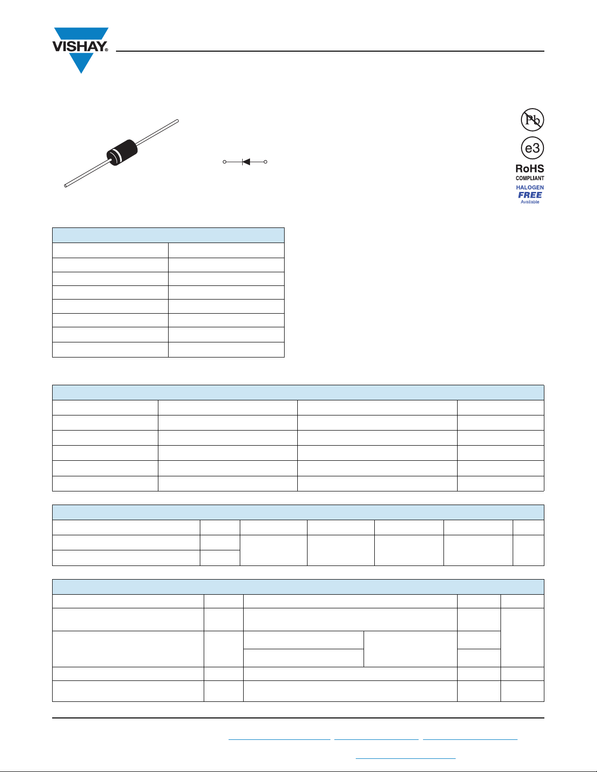
Package DO-201AD (C-16)
I
F(AV)
V
R
V
at I
F
F
I
max. 20 mA at 125 °C
RM
T
max. 150 °C
J
Diode variation Single die
E
AS
Schottky Rectifier, 3.3 A
FEATURES
• Low profile, axial leaded outline
• High frequency operation
Cathode Anode
3.3 A
30 V, 40 V
See Electrical table
6.0 mJ
• Very low forward voltage drop
• High purity, high temperature epoxy
encapsulation for enhanced mechanical
strength and moisture resistance
• Guard ring for enhanced ruggedness and
long term reliability
• Compliant to RoHS Directive 2002/95/EC
• Designed and qualified for commercial level
• Halogen-free according to IEC 61249-2-21 definition
(-M3 only)
DESCRIPTION
The VS-31DQ... axial leaded Schottky rectifier has been
optimized for very low forward voltage drop, with moderate
leakage. Typical applications are in switching power
supplies, converters, freewheeling diodes, and reverse
battery protection
Vishay Semiconductors
MAJOR RATINGS AND CHARACTERISTICS
SYMBOL CHARACTERISTICS VALUES UNITS
I
F(AV)
V
I
FSM
V
T
RRM
F
J
Rectangular waveform 3.3 A
30/40 V
tp = 5 μs sine 450 A
3 Apk, TJ = 25 °C 0.57 V
- 40 to 150 °C
VOLTAGE RATINGS
PARAMETER SYMBOL VS-31DQ03 VS-31DQ03-M3 VS-31DQ04 VS-31DQ04-M3 UNITS
Maximum DC reverse voltage V
Maximum working peak reverse voltage V
R
RWM
30 30 40 40 V
ABSOLUTE MAXIMUM RATINGS
PARAMETER SYMBOL TEST CONDITIONS VALUES UNITS
Maximum average forward current
See fig. 4
Maximum peak one cycle
non-repetitive surge current
See fig. 6
Non-repetitive avalanche energy E
Repetitive avalanche current I
I
F(AV)
I
FSM
AR
50 % duty cycle at TL = 117 °C, rectangular waveform 3.3
5 µs sine or 3 µs rect. pulse
10 ms sine or 6 ms rect. pulse 90
TJ = 25 °C, I
AS
Current decaying linearly to zero in 1 μs
Frequency limited by T
= 1.0 A, L = 12 mH 6.0 mJ
AS
maximum VA = 1.5 x VR typical
J
Following any rated load
condition and with rated
V
applied
RRM
450
1.0 A
A
Revision: 20-Sep-11
For technical questions within your region: DiodesAmericas@vishay.com
THIS DOCUMENT IS SUBJECT TO CHANGE WITHOUT NOTICE. THE PRODUCTS DESCRIBED HEREIN AND THIS DOCUMENT
ARE SUBJECT TO SPECIFIC DISCLAIMERS, SET FORTH AT www.vishay.com/doc?91000
1
, DiodesAsia@vishay.com, DiodesEurope@vishay.com
Document Number: 93319
dP
tot
dT
J
-------------
1
R
thJA
--------------<
VS-31DQ03, VS-31DQ03-M3, VS-31DQ04, VS-31DQ04-M3
www.vishay.com
ELECTRICAL SPECIFICATIONS
PARAMETER SYMBOL TEST CONDITIONS VALUES UNITS
3 A
Maximum forward voltage drop
See fig. 1
V
FM
6 A 0.71
(1)
3 A
6 A 0.62
Maximum reverse leakage current
See fig. 4
I
RM
Typical junction capacitance C
Typical series inductance L
T
S
TJ = 25 °C
(1)
T
= 125 °C 20
J
VR = 5 VDC (test signal range 100 kHz to 1 MHz) 25 °C 190 pF
Measured lead to lead 5 mm from package body 9.0 nH
Maximum voltage rate of charge dV/dt Rated V
R
T
= 25 °C
J
= 125 °C
T
J
V
= Rated V
R
Note
(1)
Pulse width < 300 μs, duty cycle < 2 %
THERMAL - MECHANICAL SPECIFICATIONS
PARAMETER SYMBOL TEST CONDITIONS VALUES UNITS
Maximum junction and storage
temperature range
Maximum thermal resistance,
junction to ambient
Typical thermal resistance,
junction to lead
Approximate weight
Marking device Case style C-16
Note
(1)
thermal runaway condition for a diode on its own heatsink
(1)
T
, T
J
Stg
R
thJA
R
thJL
DC operation
Without cooling fin
With fin 20 mm x 20 mm (0.79" x 0.79")
1.0 mm (0.04") thickness
Vishay Semiconductors
0.57
0.51
1
R
10 000 V/µs
- 40 to 150 °C
80
15
1.2 g
0.042 oz.
31DQ03
31DQ04
V
mA
°C/W
Revision: 20-Sep-11
For technical questions within your region: DiodesAmericas@vishay.com
THIS DOCUMENT IS SUBJECT TO CHANGE WITHOUT NOTICE. THE PRODUCTS DESCRIBED HEREIN AND THIS DOCUMENT
ARE SUBJECT TO SPECIFIC DISCLAIMERS, SET FORTH AT www.vishay.com/doc?91000
2
, DiodesAsia@vishay.com, DiodesEurope@vishay.com
Document Number: 93319
 Loading...