Vishay VS-30PT100 Data Sheet

Base
cathode
2
13
Anode
Cathode
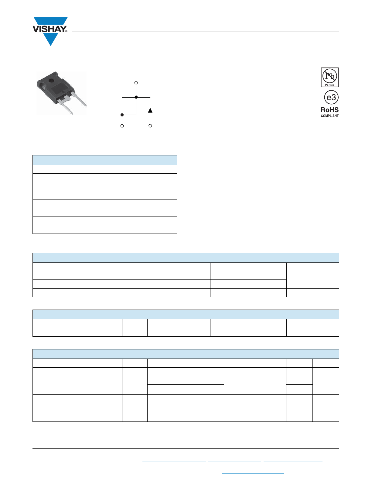
TO-247AC modified
www.vishay.com
Vishay Semiconductors
High Performance Generation 5.0 Schottky Rectifier, 30 A
FEATURES
• 175 °C high performance Schottky diode
• Very low forward voltage drop
• Extremely low reverse leakage
PRODUCT SUMMARY
Package TO-247AC modified
I
F(AV)
V
R
at I
V
F
F
I
max. 15 mA at 125 °C
RM
T
max. 175 °C
J
Diode variation Single die
E
AS
30 A
100 V
0.64 V
135 mJ
• Optimized V
• Increased ruggedness for reverse avalanche
capability
• RBSOA available
• Negligible switching losses
• Submicron trench technology
• Compliant to RoHS Directive 2002/95/EC
• Designed and qualified according to JEDEC-JESD47
APPLICATIONS
• High efficiency SMPS
• Automotive
• High frequency switching
• Output rectification
• Reverse battery protection
• Freewheeling
• DC/DC systems
• Increased power density systems
vs. IR trade off for high efficiency
F
VS-30PT100
MAJOR RATINGS AND CHARACTERISTICS
SYMBOL CHARACTERISTICS VALUES UNITS
V
V
T
RRM
F
J
30 Apk, TJ = 125 °C (typical) 0.61
Range - 55 to 175 °C
100
V
VOLTAGE RATINGS
PARAMETER SYMBOL TEST CONDITIONS VS-30PT100 UNITS
Maximum DC reverse voltage V
R
TJ = 25 °C 100 V
ABSOLUTE MAXIMUM RATINGS
PARAMETER SYMBOL TEST CONDITIONS VALUES UNITS
Maximum average forward current I
Maximum peak one cycle
non-repetitive surge current
Non-repetitive avalanche energy E
Repetitive avalanche current I
F(AV)
I
FSM
AR
50 % duty cycle at TC = 156 °C, rectangular waveform 30
5 µs sine or 3 µs rect. pulse
10 ms sine or 6 ms rect. pulse 450
TJ = 25 °C, IAS = 3 A, L = 30 mH 135 mJ
AS
Limited by frequency of operation and time pulse duration so
that T
< TJ max. IAS at TJ max. as a function of time pulse
J
See fig. 8
Following any rated load
condition and with rated
V
applied
RRM
2200
I
T
J
at
AS
max.
A
A
Revision: 10-Aug-11
1
For technical questions within your region: DiodesAmericas@vishay.com
THIS DOCUMENT IS SUBJECT TO CHANGE WITHOUT NOTICE. THE PRODUCTS DESCRIBED HEREIN AND THIS DOCUMENT
ARE SUBJECT TO SPECIFIC DISCLAIMERS, SET FORTH AT www.vishay.com/doc?91000
, DiodesAsia@vishay.com, DiodesEurope@vishay.com
Document Number: 94532

VS-30PT100
www.vishay.com
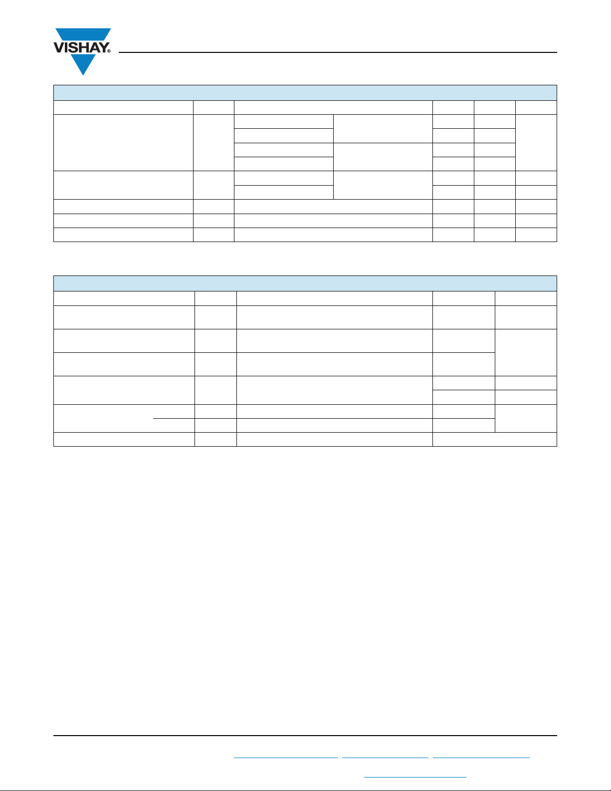
ELECTRICAL SPECIFICATIONS
PARAMETER SYMBOL TEST CONDITIONS TYP. MAX. UNITS
30 A
Forward voltage drop V
FM
(1)
30 A
60 A -0.9
60 A -0.76
Reverse leakage current I
Junction capacitance C
Series inductance L
RM
T
S
= 125 °C - 15 mA
T
J
VR = 5 VDC (test signal range 100 kHz to 1 MHz) 25 °C 1650 - pF
Measured lead to lead 5 mm from package body 7.5 - nH
TJ = 25 °C
(1)
Maximum voltage rate of change dV/dt Rated V
R
T
T
J
V
= Rated VR
R
= 25 °C
J
= 125 °C
Note
(1)
Pulse width < 300 μs, duty cycle < 2 %
THERMAL - MECHANICAL SPECIFICATIONS
PARAMETER SYMBOL TEST CONDITIONS VALUES UNITS
Maximum junction and
storage temperature range
Maximum thermal resistance,
junction to case
Typical thermal resistance,
case to heatsink
Approximate weight
Mounting torque
minimum 6 (5)
maximum 12 (10)
Marking device Case style TO-247AC modified (JEDEC) 30PT100
, T
T
J
Stg
R
DC operation 0.8
thJC
R
thCS
Mounting surface, smooth and greased 0.25
Vishay Semiconductors
-0.77
-0.64
- 200 μA
- 10 000 V/μs
- 55 to 175 °C
°C/W
6g
0.21 oz.
kgf · cm
(lbf · in)
V
Revision: 10-Aug-11
For technical questions within your region: DiodesAmericas@vishay.com
2
, DiodesAsia@vishay.com, DiodesEurope@vishay.com
Document Number: 94532
THIS DOCUMENT IS SUBJECT TO CHANGE WITHOUT NOTICE. THE PRODUCTS DESCRIBED HEREIN AND THIS DOCUMENT
ARE SUBJECT TO SPECIFIC DISCLAIMERS, SET FORTH AT www.vishay.com/doc?91000

www.vishay.com
Forward Voltage Drop - VFM (V)
Instantaneous Forward Current - I
F
(A)
0.0 0.2 0.4 0.6 0.8 1.0 1.2 1.4 1.6
1
10
100
1000
Tj = 25°C
Tj = 125°C
Tj = 175°C
Reverse Current - I
R
(mA)
Reverse Voltage - VR (V)
0 20406080100
0.001
0.01
0.1
1
10
100
75°C
100°C
50°C
125C
150°C
175°C
25°C
Reverse Voltage - VR (V)
Junction Capacitance - C
T
(pF)
0 20 40 60 80 100
100
1000
10000
VS-30PT100
Vishay Semiconductors
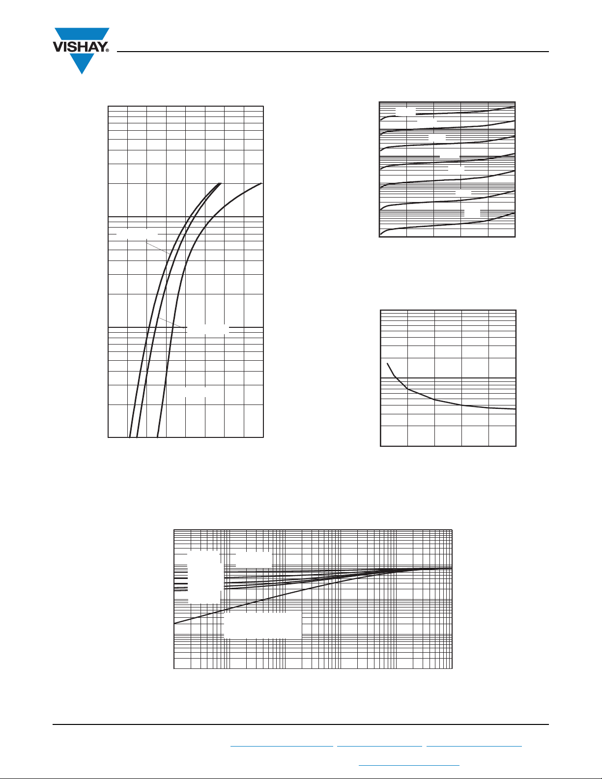
Fig. 1 - Maximum Forward Voltage Drop Characteristics
Revision: 10-Aug-11
For technical questions within your region: DiodesAmericas@vishay.com
THIS DOCUMENT IS SUBJECT TO CHANGE WITHOUT NOTICE. THE PRODUCTS DESCRIBED HEREIN AND THIS DOCUMENT
Fig. 2 - Typical Values of Reverse Current vs.
Reverse Voltage
Fig. 3 - Typical Junction Capacitance vs. Reverse Voltage
10
(°C/W)
thJC
0.1
0.01
D = 0.5
1
D = 0.33
D = 0.25
D = 0.2
D = 0.75
Single Pulse
(Thermal Resistance)
Thermal Impedance Z
0.001
1E-05 1E-04 1E-03 1E-02 1E-01 1E+00
t1, Rectangular Pulse Duration (Seconds)
Fig. 4 - Maximum Thermal Impedance Z
Characteristics
thJC
3
, DiodesAsia@vishay.com, DiodesEurope@vishay.com
ARE SUBJECT TO SPECIFIC DISCLAIMERS, SET FORTH AT www.vishay.com/doc?91000
Document Number: 94532
 Loading...