

Vishay VS-30CTQ...SPbF Series, VS-30CTQ...-1PbF Series Data Sheet
A
VS-30CTQ...SPbF, VS-30CTQ...-1PbF Series
Vishay High Power Products
Schottky Rectifier, 2 x 15 A
VS-30CTQ...SPbF
VS-30CTQ...-1PbF
FEATURES
• 175 °C TJ operation
• Center tap TO-220 package
• Very low forward voltage drop
• High frequency operation
• High purity, high temperature epoxy
Base
common
cathode
2
Base
common
cathode
2
encapsulation for enhanced mechanical
strength and moisture resistance
• Guard ring for enhanced ruggedness and long
term reliability
• Meets MSL level 1, per J-STD-020, LF maximum peak of
260 °C
1
node Anode
2
Common
cathode
2
D
PAK
3
1
Anode Anode
2
Common
cathode
TO-262
3
• Halogen-free according to IEC 61249-2-21 definition
• Compliant to RoHS directive 2002/95/EC
• AEC-Q101 qualified
DESCRIPTION
The VS-30CTQ... center tap Schottky rectifier has been
PRODUCT SUMMARY
I
F(AV)
V
R
2 x 15 A
35 V to 45 V
optimized for very low forward voltage drop, with moderate
leakage. The proprietary barrier technology allows for
reliable operation up to 175 °C junction temperature. Typical
applications are in switching power supplies, converters,
freewheeling diodes, and reverse battery protection.
MAJOR RATINGS AND CHARACTERISTICS
SYMBOL CHARACTERISTICS VALUES UNITS
I
F(AV)
V
I
FSM
V
T
RRM
F
J
Rectangular waveform 30 A
35 to 45 V
tp = 5 μs sine 1060 A
15 Apk, TJ = 125 °C (per leg) 0.56 V
Range - 55 to 175 °C
VOLTAGE RATINGS
PARAMETER SYMBOL
Maximum DC reverse voltage V
Maximum working peak reverse voltage V
R
RWM
VS-30CTQ035SPbF
VS-30CTQ035-1PbF
35 40 45 V
VS-30CTQ040SPbF
VS-30CTQ040-1PbF
VS-30CTQ045SPbF
VS-30CTQ045-1PbF
UNITS
ABSOLUTE MAXIMUM RATINGS
PARAMETER SYMBOL TEST CONDITIONS VALUES UNITS
Maximum average forward current
See fig. 5
Maximum peak one cycle
non-repetitive surge current per leg
See fig. 7
Non-repetitive avalanche energy per leg E
Repetitive avalanche current per leg I
Document Number: 94188 For technical questions, contact: diodestech@vishay.com
Revision: 12-Mar-10 1
I
F(AV)
I
FSM
AR
50 % duty cycle at TC = 127 °C, rectangular waveform 30
5 μs sine or 3 μs rect. pulse
10 ms sine or 6 ms rect. pulse 265
TJ = 25 °C, IAS = 3.0 A, L = 4.40 mH 20 mJ
AS
Current decaying linearly to zero in 1 μs
Frequency limited by T
maximum VA = 1.5 x VR typical
J
Following any rated load
condition and with rated
V
applied
RRM
1060
3.0 A
www.vishay.com
A
VS-30CTQ...SPbF, VS-30CTQ...-1PbF Series
Vishay High Power Products
Schottky Rectifier, 2 x 15 A
ELECTRICAL SPECIFICATIONS
PARAMETER SYMBOL TEST CONDITIONS VALUES UNITS
15 A
Maximum forward voltage drop per leg
See fig. 1
V
FM
30 A 0.76
(1)
15 A
30 A 0.70
Maximum reverse leakage current per leg
See fig. 2
I
RM
Maximum junction capacitance per leg C
Typical series inductance per leg L
TJ = 25 °C
(1)
T
= 125 °C 15
J
VR = 5 VDC (test signal range 100 kHz to 1 MHz), 25 °C 900 pF
T
Measured lead to lead 5 mm from package body 8.0 nH
S
Maximum voltage rate of change dV/dt Rated V
T
= 25 °C
J
= 125 °C
T
J
V
= Rated V
R
R
R
0.62
0.56
2
10 000 V/μs
Note
(1)
Pulse width < 300 μs, duty cycle < 2 %
THERMAL - MECHANICAL SPECIFICATIONS
PARAMETER SYMBOL TEST CONDITIONS VALUES UNITS
Maximum junction and storage
temperature range
Maximum thermal resistance,
junction to case per leg
Maximum thermal resistance,
junction to case per package
Typical thermal resistance,
case to heatsink
Approximate weight
Mounting torque
Marking device
minimum 6 (5)
maximum 12 (10)
T
, T
J
Stg
DC operation
See fig. 4
R
thJC
- 55 to 175 °C
3.25
DC operation 1.63
R
thCS
Mounting surface, smooth and greased 0.50
2g
0.07 oz.
kgf ⋅ cm
(lbf ⋅ in)
Case style D
2
PAK 30CTQ045S
Case style TO-262 30CTQ045-1
V
mA
°C/W
www.vishay.com For technical questions, contact: diodestech@vishay.com
Document Number: 94188
2 Revision: 12-Mar-10
VS-30CTQ...SPbF, VS-30CTQ...-1PbF Series
Schottky Rectifier, 2 x 15 A
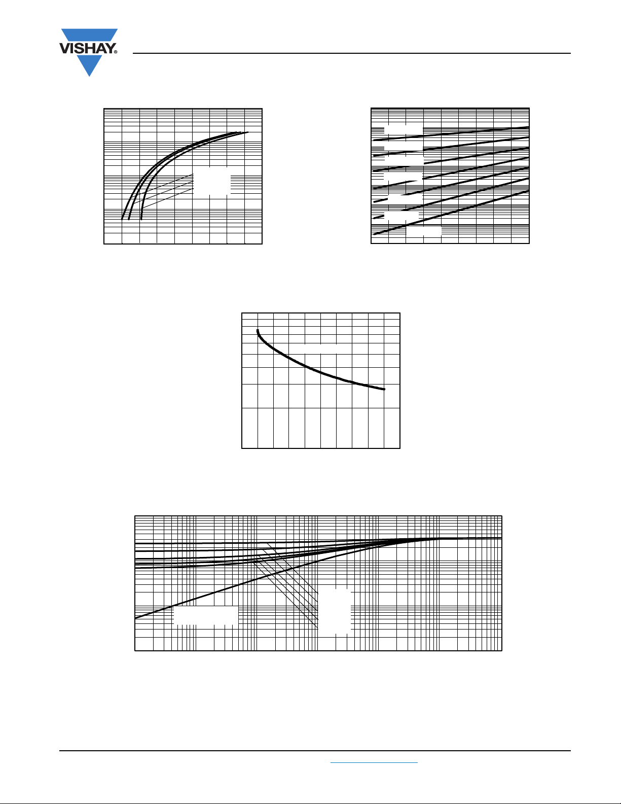
1000
100
(Per Leg)
TJ =175° C
=125° C
T
J
T
= 25° C
J
1000
1.4 1.6 1.80 0.2 0.4 0.6 0.8 1.0 1.2
10
Current (A)
1
- Instantaneous Forward
F
I
0.1
V
- Forward Voltage Drop (V)
FM
Fig. 1 - Maximum Forward Voltage Drop Characteristics
TJ = 25 °C
Vishay High Power Products
1000
100
0.01
- Reverse Current (mA)
R
I
0.001
0.0001
TJ = 175 °C
TJ = 150 °C
10
TJ = 125 °C
1
TJ = 100 °C
0.1
TJ = 75 °C
TJ = 50 °C
TJ = 25 °C
V
- Reverse Voltage (V)
R
Fig. 2 - Typical Values of Reverse Current vs.
Reverse Voltage (Per Leg)
30 35 40 450 5 10 15 20 25
- Junction Capacitance (pF)
T
C
100
10 20 30 40 500
V
- Reverse Voltage (V)
R
Fig. 3 - Typical Junction Capacitance vs. Reverse Voltage (Per Leg)
10
1
D = 0.75
0.1
- Thermal Impedance (°C/W)
thJC
Z
0.01
0.00001 0.0001 0.001 0.01 0.1 1
Single pulse
(thermal resistance)
D = 0.50
D = 0.33
D = 0.25
D = 0.20
t1 - Rectangular Pulse Duration (s)
Fig. 4 - Maximum Thermal Impedance Z
Characteristics (Per Leg)
thJC
1.0
Document Number: 94188 For technical questions, contact: diodestech@vishay.com
www.vishay.com
Revision: 12-Mar-10 3
 Loading...